E-beam-transparent SiN membranes with thicknesses ranging from 15 nm to 200 nm are available commercially and are among the most commonly used support films for imaging nanoparticles in TEM [
15]. We used them as substrates, onto which superconducting and ferromagnetic films were deposited and nanostructured. As a practical alternative, we used 200 µm thick Si substrates that were buffered on both sides by 40 nm thick SiN films using low-pressure chemical vapor deposition (LPCVD). In the latter case, the superconducting and ferromagnetic films were deposited and nanostructured under standard conditions on bulk substrates, followed by wet chemical etching of the Si substrate in 20% KOH from the back side of the substrate to the back side of the SiN buffer layer using commercial wafer holders [
16]. Alternatively, and more commonly, home-made analogues for etching substrates with standard sizes of 10 mm × 10 mm × 0.3 mm or 20 mm × 20 mm × 0.3 mm are used. The measured etch rate of Si in a 20% solution of KOH in water was approximately 9 nm/h. This etch rate can be compared with the 6 µm/min etch rate of the Si substrate by reactive ion etching (RIE) enhanced by an inductively coupled plasma (ICP) and performed in pure SF
6 gas [
17].
2.1. Superconducting Nanostructures
The substrates were cleaned in acetone, propanol, and deionized water and etched with an Ar+ ion beam just before placing them in a home-built sputtering machine, which was evacuated to a base pressure of <4 × 10⁻⁸ mbar using oil-free pumps. TiN and NbN films were deposited at a rate of ~3 nm/min from 50 mm 99.95% pure TiN and NbN targets using pulsed reactive DC magnetron sputtering. The substrates were lying freely on a heater. The heater temperature was 920 °C during TiN deposition and 800 °C during NbN deposition. Deposition was performed in an Ar(80%)-N2(20%) gas mixture at a total pressure of 10−2 mbar. A N2 flow of 5 mln/min was regulated using a Brooks© 5850 TR mass flow controller. Ar and N2 gases had a purity of 99.9999% and contained less than 0.01 ppm O2, which corresponds to an O2 partial pressure of less than 10−10 mbar. Before deposition, the chamber was outgassed under deposition conditions during pre-sputtering onto the closed shutter for more than 1 h.
A thin-film TiN-NbN-TiN multilayer heterostructure was used for the preparation of superconducting nanowires, Dayem-type nJJs, and nanoSQUIDs. As shown in ref. [
18] and ref. [
19], TiN and NbN thin films exhibit good superconducting properties when they are deposited onto an LPCVD SiN buffer layer and grown epitaxially on top of each other. The lattice constants of TiN and NbN are 0.424 nm and 0.439 nm, respectively. The lowest 3 nm thick TiN layer served as a buffer layer for the subsequent NbN film and improved its
Tc and critical current. The uppermost 15 nm thick TiN layer in the TiN-NbN-TiN heterostructure served for the fine setting of
Tc and for the protection of the 15 nm thick NbN layer from corrosion and oxidation during patterning by EBL and subsequent resist removal using warm acetone.
The insertion of the superconducting NbN layer in between two TiN layers allows the
Tc value of the heterostructure to be tuned for the improved operation of nJJs at the stabilized temperature of the TEM sample holder. This insertion also reduces the width of the superconducting transition in the
R(
T) dependence. The latter behavior reflects a reduction in thermally activated flux motion and a higher critical current density in such a heterostructure. Additional passivation by a thin Si layer can also improve the thermal sink and provide protection against the mechanical and electrical fragility of the devices. The
R(
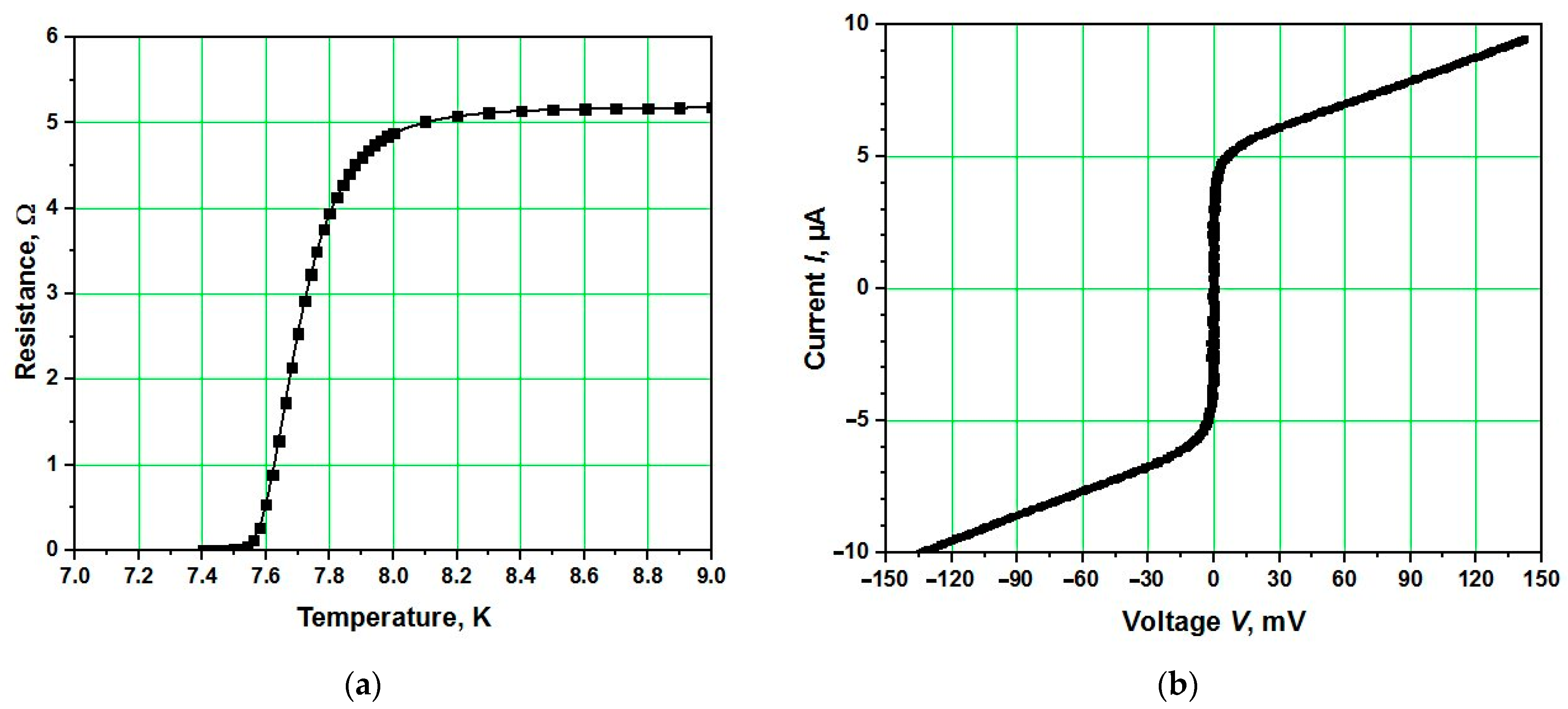
T) dependence of the TiN(3 nm)-NbN(15 nm)-TiN(15 nm)-Si(330 nm) heterostructure measured using Quantum Design (QD) Physical Property Measurement Systems (PPMS) is shown in
Figure 1a. The heterostructure has
Tc ≅ 7.5 K, while the superconducting transition temperatures of TiN and NbN films of thicknesses >200 nm deposited under similar conditions were 5 and 16 K, respectively. The
Tc ≅ 7.5 K value for the heterostructure is smaller than the
Tc value for NbN films of similar thickness due to the proximity effect with the covering TiN film, but it is optimal for non-hysteretic operation of nJJs and nanoSQUID at the operating temperature of 5 K, which can be realized in a TEM sample holder.
Figure 1b shows non-hysteretic
I(
V) dependence measured for a 30 nm wide TiN-NbN-TiN nJJ at 5 K. Non-hysteretic
I(
V) characteristics of nJJs are required for the use of conventional readout techniques to operate nanoSQUIDs as magnetic flux-to-voltage converters. The critical current
Ic ≅ 5 µA and the normal state resistance
Rn ≅ 30 Ω correspond to current density in the Nb layer of
Jc ≅ 1 MA/cm
2 and a characteristic voltage of the nJJ of
Vc =
IcRn ≅ 150 µV. A nanoSQUID with such nJJs demonstrates peak-to-peak quantum oscillations in its
V(
B) characteristics with an amplitude of up to ~20 µV, as shown in
Figure 2.
The Ginzburg–Landau coherence length
is the characteristic scale over which spatial variations in the superconducting order parameter occur. Constriction of a size smaller than the “critical” length, i.e.,
Lc = 3.49
ξ, patterned in a superconducting film behaves as Josephson junctions [
6,
20]. By measuring the resistance of the TiN-NbN-TiN heterostructure as a function of the magnetic field using the QD PPMS at 4.2 K, we determined a critical magnetic field of
Bc2 ≅ 7 T and the superconducting coherence length
ξ(4.2 K) ≅
≅ 6 nm. This coherence length corresponds to
Lc ≅ 30 nm at 6 K, which in turn corresponds to the current thickness of the TiN-NbN-TiN heterostructure and the typical width and length of nJJs that we can achieve using EBL. The coherence length in the TiN-NbN-TiN heterostructure is slightly larger than that in NbN films of a similar thickness due to the proximity effect of the TiN film.
Patterning of the 30 nm thick TiN-NbN-TiN heterostructures was performed using highly selective RIE with pure SF
6 gas and 100 nm thick masks of AZ nLof2020 resist, diluted by AZ EBR thinner with a ratio of 1:3. When compared with masks of diluted HSQ resist [
21], diluted nLof2020 resist has the advantages of requiring a ~10 times lower dose of electron-beam exposure and its residuals after RIE can be removed by easily using warm acetone. A passivating Si layer was deposited after removal of the resist residuals for improved coverage of the completed patterned structures. The use of pure SF6 gas in RIE provides several benefits when compared to physical etching using an Ar+ ion beam, including ~3 times faster etch rates for TiN and NbN in comparison to SiN and the diluted nLof2020 resist, no formation of fences due to redeposition, and a slight undercut. The 30 nm thick TiN-NbN-TiN heterostructures have an undercut of ~10 nm, which is ~3 times smaller than the undercut observed in the preparation of pure 100 nm thick TiN nJJs [
22]. The smaller undercut resulted in improved reproducibility of the nJJs and a spatial resolution of the superconducting nanostructures that approached the spatial resolution of the mask of the electron-beam resist.
EBL, high-selectivity RIE with pure SF
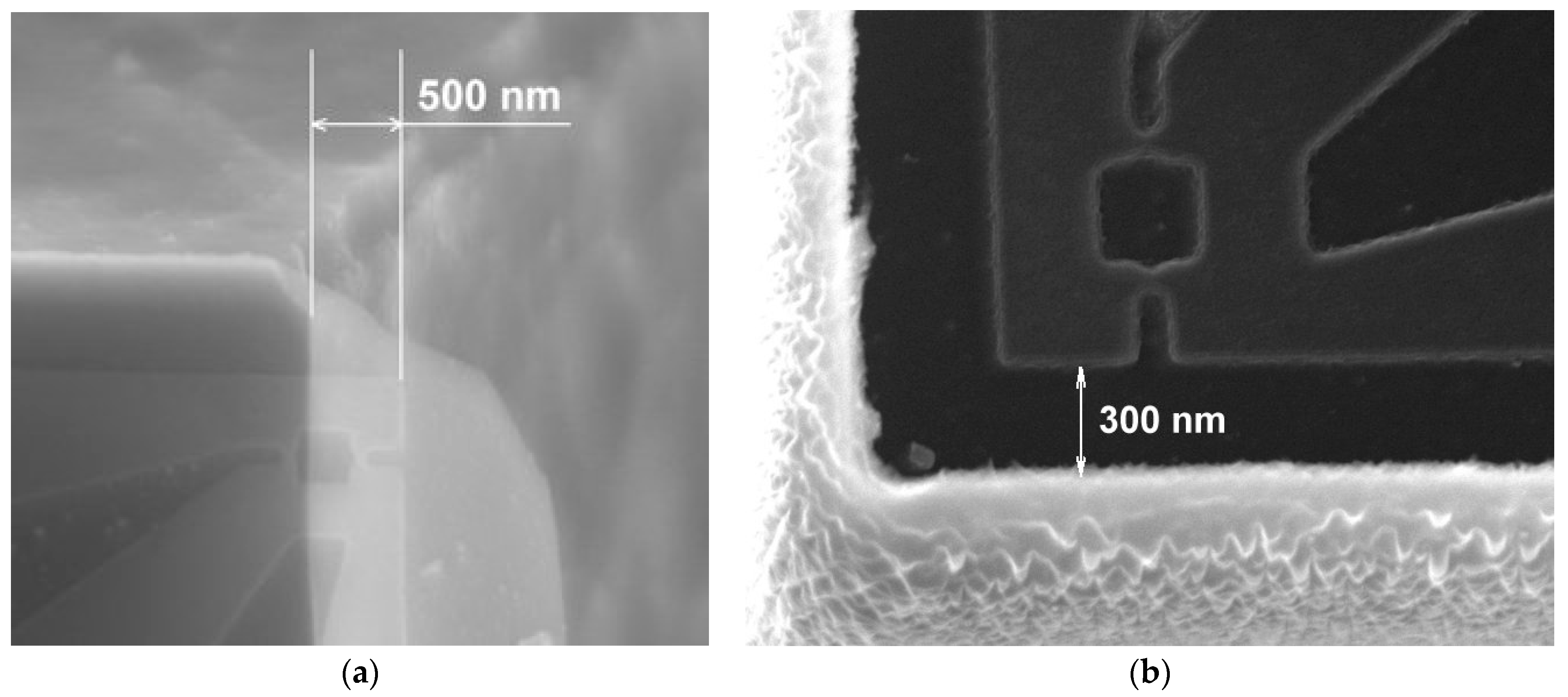
6 gas, and a naturally created undercut in the Si substrate were used to prepare nanoSQUIDs on a SiN membrane within ~500 nm of the edge of the substrate, similar to the results demonstrated in [
17] on a 10 nm thick SiO
2 membrane (see
Figure 3a). Another potential option is to place a nanoSQUID near the corner or edge of a small substrate and integrate it in a TEM sample holder.
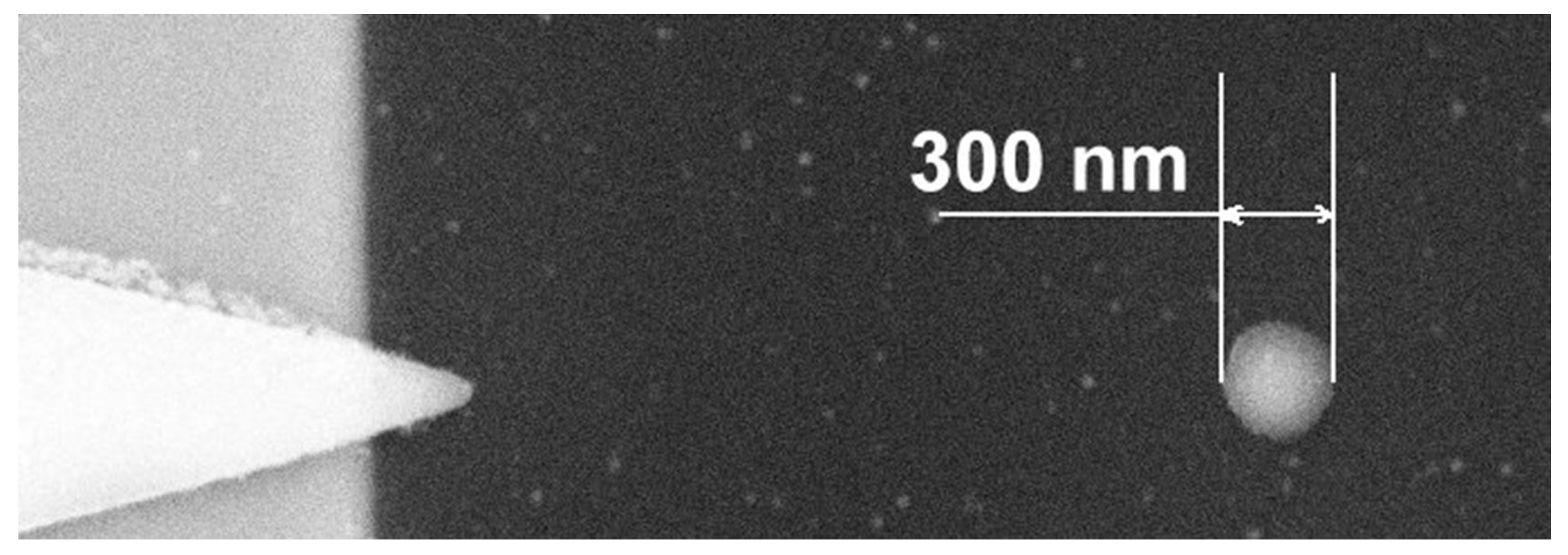
Figure 3b shows an SEM image of a planar nanoSQUID with nJJs structured using RIE, placed at a distance of ~300 nm from the edges of a 2 mm × 2 mm × 0.05 mm substrate using focused ion beam (FIB) nanosculpturing and an Al sacrificial layer. The object under study can be placed near the nanoSQUID, for example, on an electron-beam-transparent membrane or TEM grid in a flip-chip configuration. Such a configuration has the advantage of better heat removal from the nJJs and nanoSQUID during their operation in a finite-voltage state. The achieved 300 nm separation of planar nanoSQUIDs from the substrate corner can be compared with the state-of-the-art approximately 10 µm distance that was demonstrated in [
23].
If heat removal from the operating nJJs and nanoSQUID is insufficient, then thermal hysteresis of the
I(
V) characteristics occurs. Thermal hysteresis is a result of overheating of the nJJ when its superconducting current exceeds the critical current. The dissipated energy then heats the nJJ above
Tc, so that the nanobridge enters the normal conducting state [
24]. As a result of Joule heat dissipated on the normal conducting nanobridge, its temperature also rises, which in turn reduces the retrapping critical current
Ir. The ratio of
Ic to
Ir depends on thermal coupling between the nJJ and the substrate and is greater in the case of poor heat removal (for example, in the case of free-standing nJJs or nJJs on membranes). Pure thermal hysteresis occurs when the bias current is close to the depairing current of the superconducting film, which is typically higher than the combined critical currents of the nJJs in the nanoSQUID. However, this effect cannot be used to measure magnetic fields because it does not depend on magnetic flux through the loop of the nanoSQUID [
18].
Other nanofabrication methods, which are described in the next section, are currently also used for the preparation of nanostructures of other superconducting materials, such as Al and YBCO, which cannot be structured by RIE on bulk substrates. It is possible that in the future, these methods will also be used for the preparation of superconducting nanostructures on membranes for applications in TEM. In the case of YBCO, the membrane can be made from, for example, SrTiO
3 (STO); epitaxial growth of STO on Si and its use as a buffer layer have been demonstrated in [
25]. High-quality YBCO films can be grown on STO buffer layers and should not be too thick to be electron-beam-transparent in TEM, as well as to avoid cracks due to the different thermal expansion coefficients of YBCO and Si.
2.2. Permalloy Nanostructures
Permalloy is a Ni-Fe alloy that contains ~80% Ni and ~20% Fe and is compatible with CMOS applications [
26], making it a preferred choice for ferromagnetic materials in electronics. In addition, permalloy is a soft magnetic material with small coercivity [
27], high permeability, and high saturation magnetization [
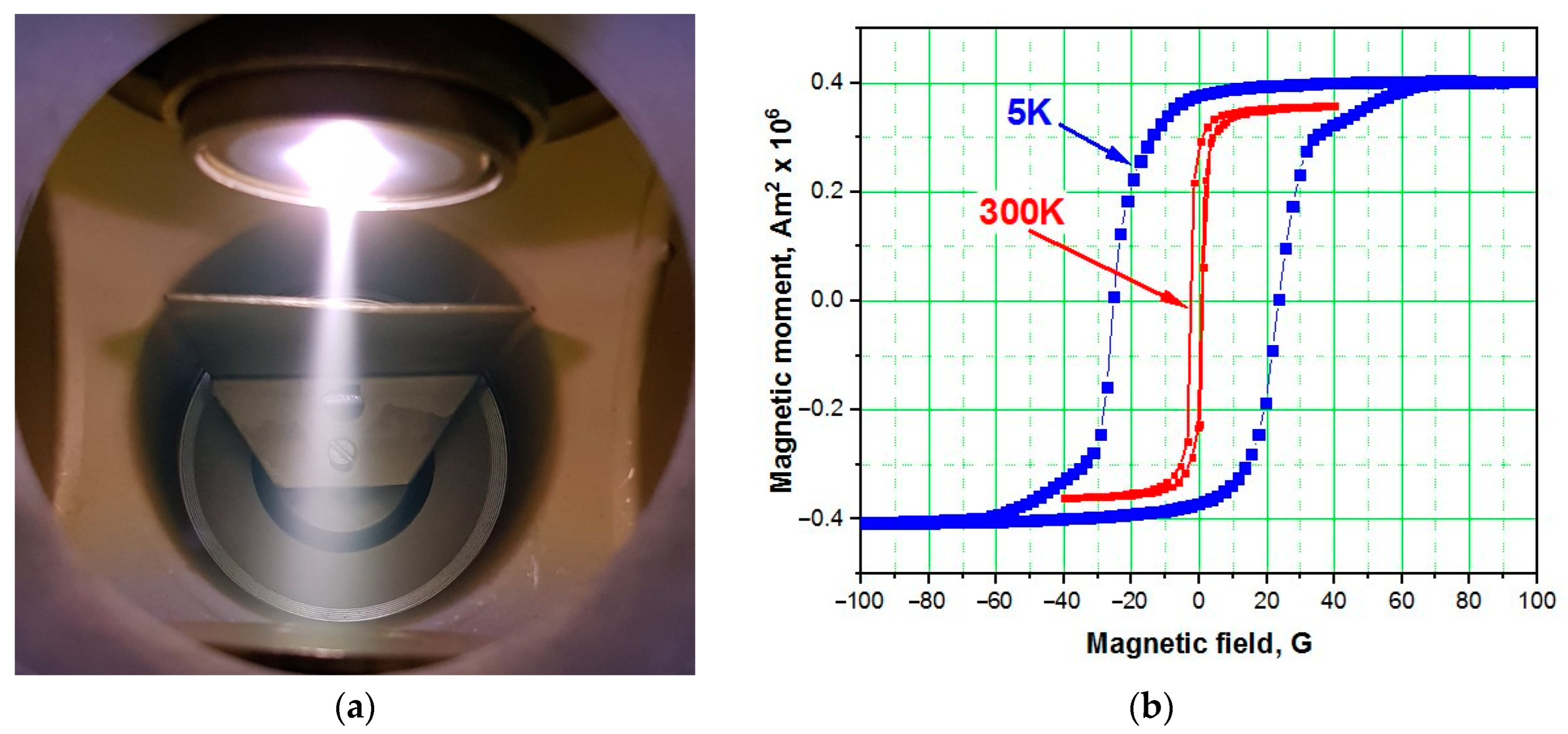
28]. We deposited thin films of permalloy at room temperature using dc magnetron sputtering from a single target in a pure Ar atmosphere at a pressure of ~1 Pa. The permalloy target had a diameter of 35 mm, but the intense plasma was only produced in an area of diameter ~8 mm using a special arrangement of a wide-ring magnet and a small-diameter Fe guide for the magnetic flux, as shown in
Figure 4a. For a target–substrate distance of ~8 cm, the sputtered material approaches the substrate almost as a parallel beam, which is advantageous for the use of shadow/stencil masks for the fabrication of permalloy nanostructures.
Figure 4b shows
M(
H) dependences measured from a 5 mm × 4 mm × 40 nm permalloy film deposited using this method, revealing coercive fields of 2 and 22 G at temperatures of 300 and 5 K, respectively.
In principle, permalloy thin films can be nanostructured using RIE enhanced by an inductively coupled plasma (ICP) [
29]. However, due to possible contamination of the available RIE machine, this method of patterning is undesirable. Instead of RIE, we prepared permalloy nanostructures using three different fabrication methods that were adapted for deposition on 40 nm thick SiN membranes: (1) lift-off; (2) ion beam etching (IBE); and (3) stencil lithography. These methods and the obtained results are described in the following three subsections.
2.2.1. Lift-Off
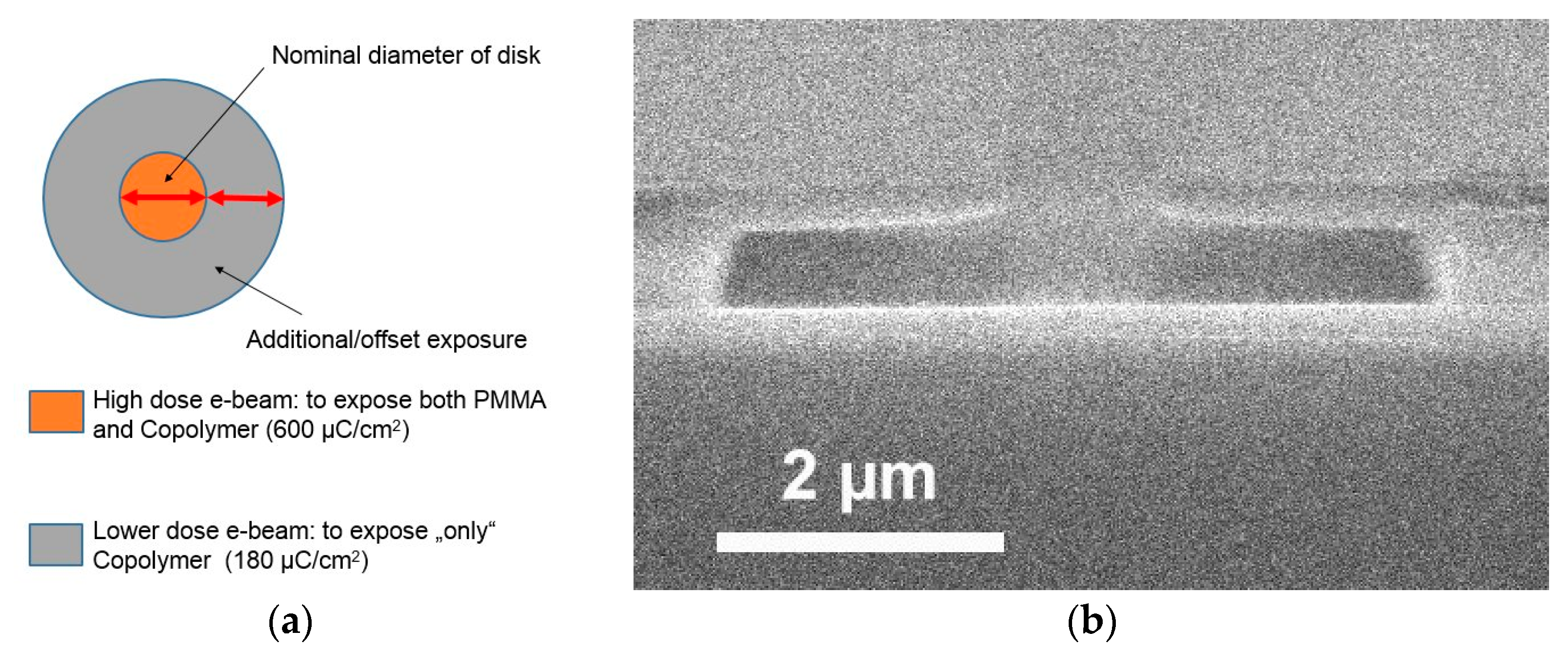
We used a bilayer of PMMA positive electron-beam resist to create an undercut structure, which ensures a clean lift-off process. The lower copolymer PMMA AR-P 617-08 (33%) layer has thickness of ~400 nm and required an electron-beam exposure dose of 180 µC/cm
2. The upper resist PPMA AR-P 679.04 (950 K) layer had a thickness of ~300 nm and required an e-beam exposure dose of 600 µC/cm
2. A nominal diameter of up to 1 µm was exposed with the highest dose, while a lower dose was used for additional-offset electron-beam exposure of the pattern to achieve a larger undercut, as shown in
Figure 5a. In both cases, the accelerating voltage of the electron beam was 100 kV, which provided penetration of the electron beam through the entire 0.7 µm thickness of the bilayer resist and its homogeneous exposure.
After 15 min of development of the bilayer PMMA resist in the AR 600-56 (MIBK) developer, an undercut that was up to 2 µm deep was achieved, as shown in
Figure 5b. The result of the offset exposure and long development time was controlled by observing a cross-section of the bilayer resist mask using scanning electron microscopy (SEM) in snapshot mode to avoid the flow and fall of the overhanging areas of the resist mask. This approach resulted in a reduced quality of the SEM image. Similar masks with a large undercut and a lift-off method can be used for double-angle shadow evaporation of Al for the in situ preparation of three-layer Al tunnel junctions for quantum bits.
Flow of the PMMA resist mask occurs at a relatively low temperature of approximately 120 °C. This temperature can be reached unintentionally in the case of insufficient heat removal from the sample during deposition of the permalloy film. Apiezon
® vacuum grease was used for thermal contact between the back side of the substrate and a massive metal plate that served as a sample holder. After deposition of the permalloy film, residuals of the Apiezon
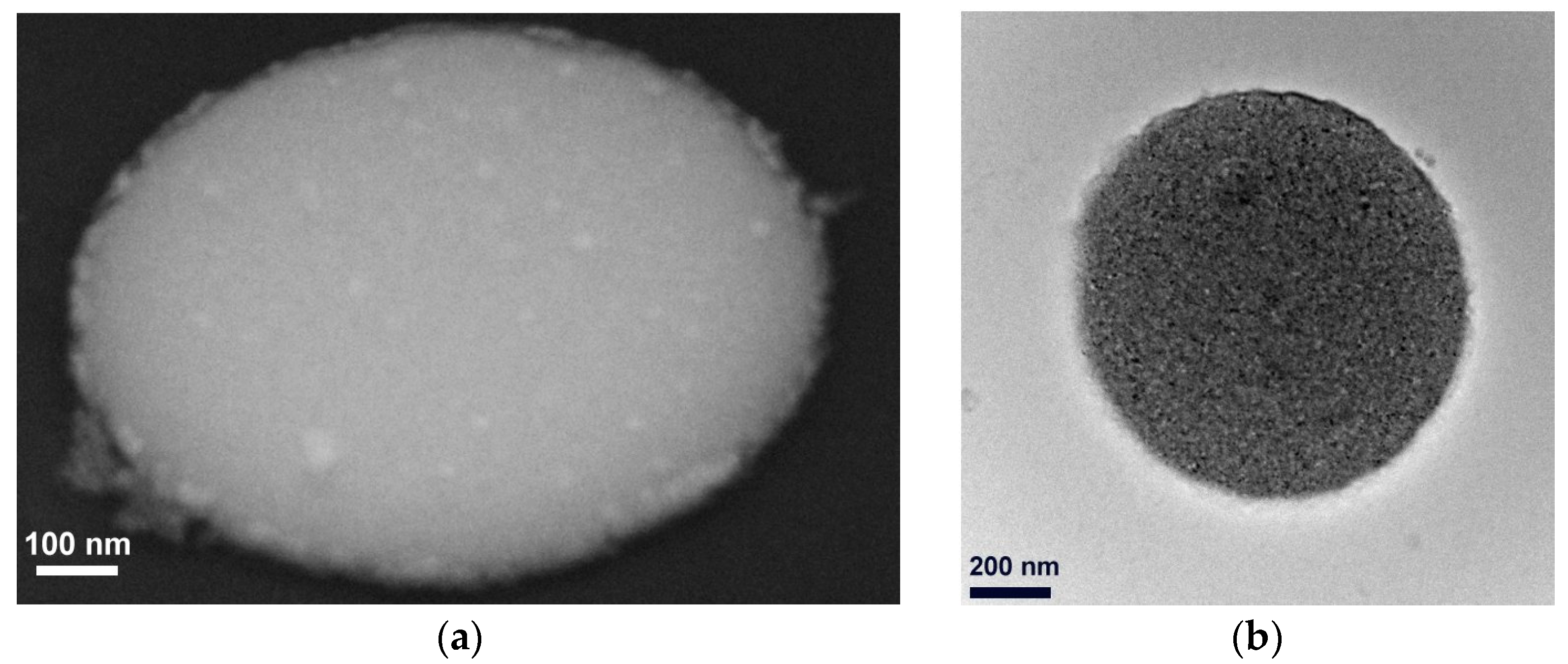
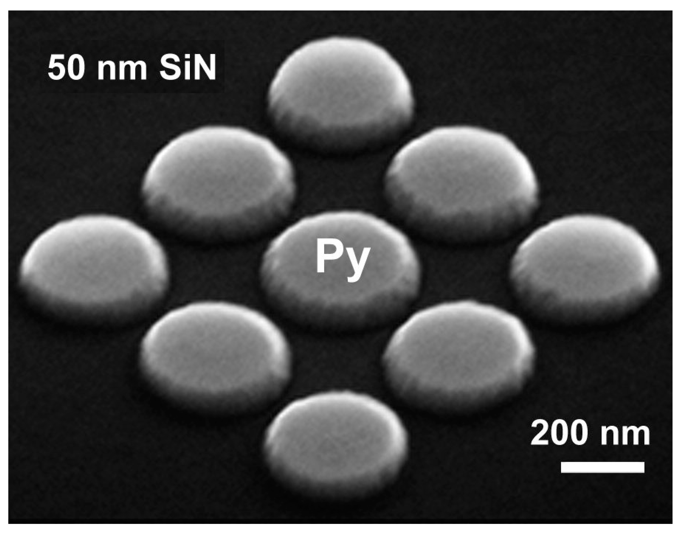
® vacuum grease were removed using Limonene solvent and the lift-off process was performed in acetone at 70 °C. The SEM and TEM images of the resulting permalloy nanodots are shown in
Figure 6.
During lift-off, the metal on the resist was washed off by placing the sample in acetone while the desired pattern remained attached to the substrate where there is a resist opening. As a result of the large undercut, the lift-off process takes place with almost no debris at the edges of the nanodots, in contrast to the case where a single-layer positive resist mask is used. Smooth edges of the nanodots are preferred because their coercivity increases with edge roughness [
30]. Several holes in the upper layer of the bilayer resist mask can share the same opening in the lower layer, allowing dense arrays of permalloy nanodots to be produced, as shown in
Figure 7a.
High-resolution TEM images of permalloy nanodisks revealed polycrystalline films with arbitrary grain orientations, an average grain size of ~5 nm, and a lattice constant of ~0.36 nm, as shown in
Figure 7b.
Figure 8 shows an SEM image of a 50 nm thick SiN membrane with a 300 nm permalloy nanodisk. The membrane area is darker in the SEM image.
2.2.2. Ion Beam Etching
IBE is a dry physical etching technique, which potentially provides a better spatial resolution than the lift-off method described above. A 200 nm thick mask from negative AZ nLof2020 resist diluted with AZ EBR solvent in a 1:2 ratio was used for the preparation of permalloy nanodisks on membranes. An Ar+ ion beam at normal incidence to the substrate surface was used to etch 100 nm thick permalloy films, while an electron-beam-patterned negative resist mask preserved the desired structure. The substrate was clamped to a water-cooled, rotating metal plate. Redeposited material created fences at the edges of the structures, which could affect the magnetic properties of the nanodisks and were removed using an additional IBE step performed at a grazing angle of ~5° after removal of the residual resist using warm acetone. In order to minimize membrane etching, the etching time was chosen so that, after IBE first performed in a direction perpendicular to the substrate surface, a few nm thick permalloy film still remained on the open surface areas, which was then removed during a second IBE step at a grazing angle.
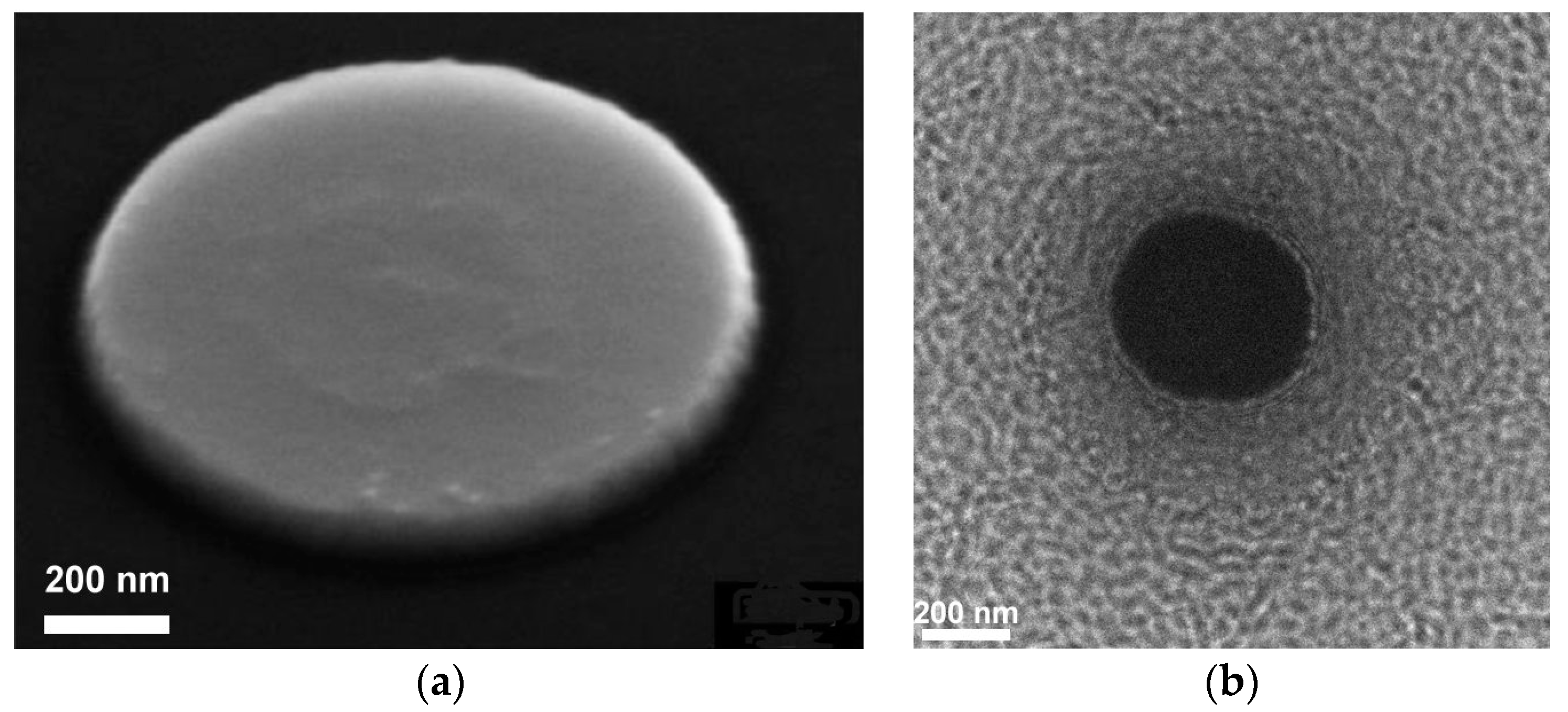
Figure 9 shows images of 100 nm thick permalloy disks made by IBE: (a) SEM image of a disk with a diameter of 900 nm; and (b) a TEM image of a disk with a diameter of 500 nm. It was observed that IBE resulted in better reproducibility of cylinder-shaped disks, with an absence of half shadow edge smoothing and debris (
Figure 9a), but led to inhomogeneous etching of the membrane. After IBE, the opened membrane areas demonstrated increased roughness and remained thicker near the nanodots due to the reduced etch rate near the structures and the redeposition of the permalloy (see
Figure 9b). The significantly thinner membrane away from the nanostructures can weaken the total mechanical stability of the entire membrane.
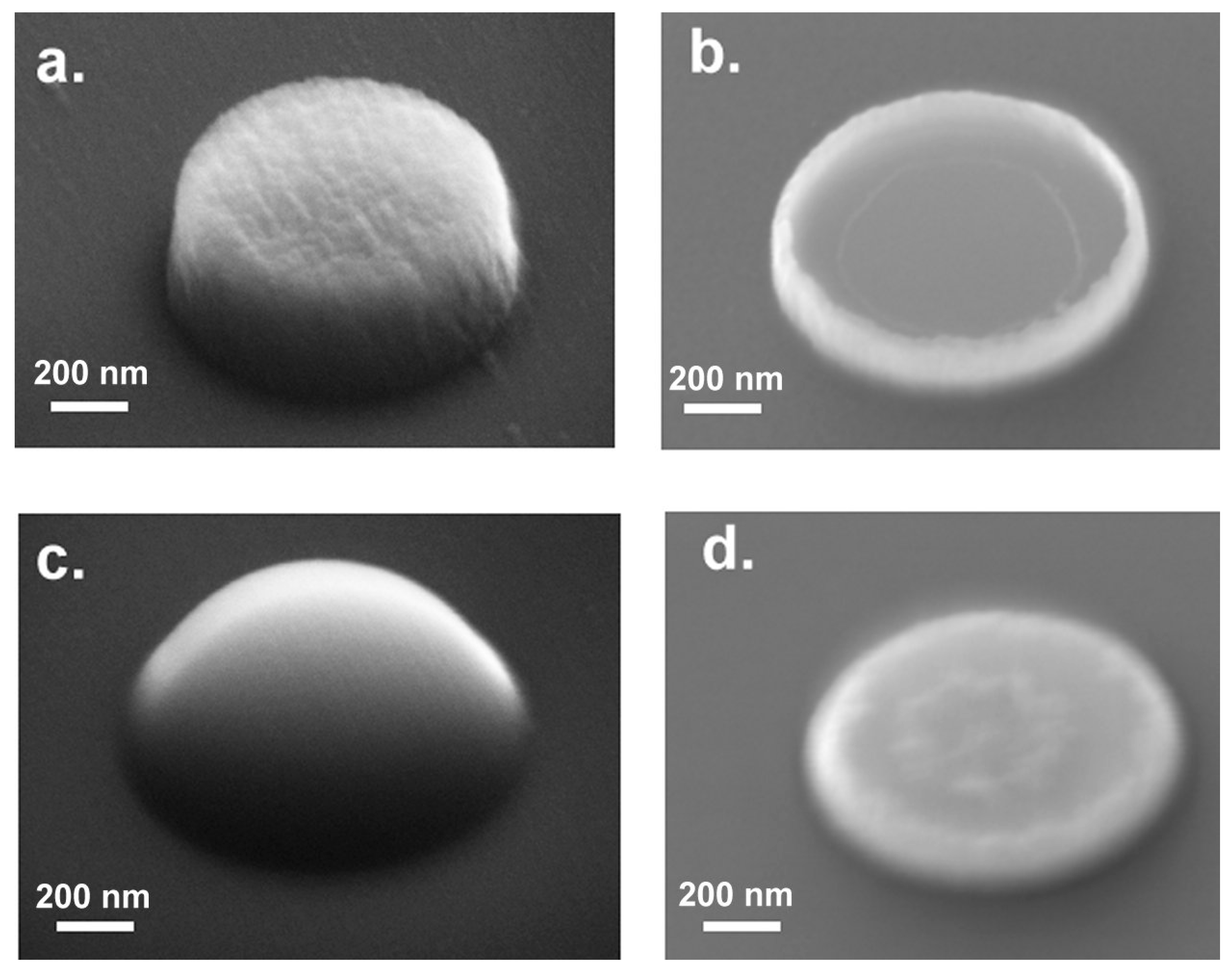
The formation of fences during IBE was reduced using a reflowed resist mask by heating it above the resist softening point. For this purpose, the samples were kept with the resist mask on a heater plate for 5 min at 150 °C before etching, as shown in
Figure 10a–d. This process changed the shape of the top surface of the resist as a result of surface tension, similarly to the meniscus of a drop of water, while maintaining the diameter of the disk near the substrate surface. Due to the tilted resist surface at the edges, there was much less redeposited material on it, and it was partially removed during IBE. Although some residue was still present after IBE when using such a reflow resist mask, this was found to be useful for minimizing redeposition and creating much shorter fences, thereby reducing the time required for additional etching and maintaining the mechanical stability of the free-standing membrane.
Arrays of nanodots were produced using IBE, as shown in
Figure 11. The reduced etch rate near each nanodot in the array led to a further reduction in the thickness of the membrane far from the array. Mutual shadowing of the fences also interfered with their removal using IBE at a grazing angle.
In general, when compared with lift-off, IBE resulted in cleaner and more controllable/reproducible structures with better spatial resolution, especially in the case of etching of much thinner films, which allowed for a much thinner resist to be used. However, the reduced thickness of the membrane away from the structures after IBE can degrade its mechanical stability.
2.2.3. Stencil Lithography
Ideally, the nanostructures should be deposited directly on an extremely thin membrane, such as 1-atom-thick graphene, without being affected by wet lithography or dry etching that can contaminate and degrade the surfaces and destroy the membrane. The use of shadow masks (stencils) can potentially solve this problem if sufficient spatial resolution is provided. Stencil lithography has been developed widely in recent years and has been used to achieve sub µm sized apertures and structures [
31,
32,
33,
34]. It is based on stencils with nanometer-sized apertures milled into a SiN membrane using, for example, FIB milling. The membrane can be identical to the membrane, on to which the films should be deposited. This method is compelling, not only because it avoids the use of EBL and any related chemical and etching processes, but also because the mask is reusable.
We prepared shadow masks based on 40 nm thick SiN membranes. Prior to milling holes using FIB milling, each membrane was covered by a 500 nm thick layer of Al for protection from undesired etching during secondary electron imaging with excitation by Ga
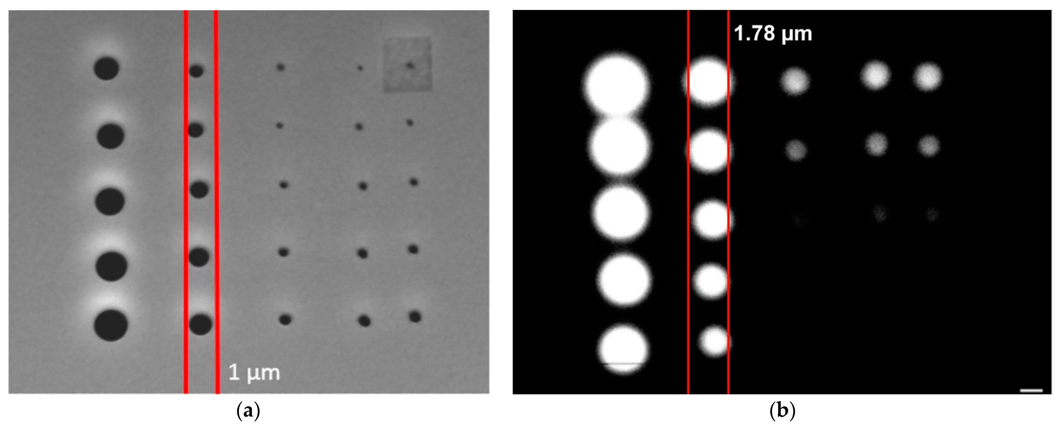
+ ions, as well as stigmatism and focus alignment of the ion beam before milling. The stencil and sample were aligned and fixed in a flip-chip configuration under an optical microscope in transient illumination. Spacers that were 500 nm thick were made on the stencil from an Al film beyond the membrane area and separated from the sample. The resulting stencil and permalloy nanodisks deposited through the mask are shown in
Figure 12a,b, respectively.
The spatial resolution achieved using our home-made stencils was ~200 nm and was limited primarily by the stencil–sample separation, which included not only the thickness of the Al spacers but also bending of the perforated membrane and possible contamination of the surfaces by sub µm sized debris. Further optimization of the preparation of the stencil mask and the alignment of the stencil and sample in clean-room conditions promise to provide a controllable separation between the stencil and sample and to significantly improve the spatial resolution and reproducibility of this method in the future.
