
Designing Large Two-Dimensional Arrays of Josephson Junctions for RF Magnetic Field Detection

 , , ,
, , ,
Abstract
:1. Introduction
2. Principle
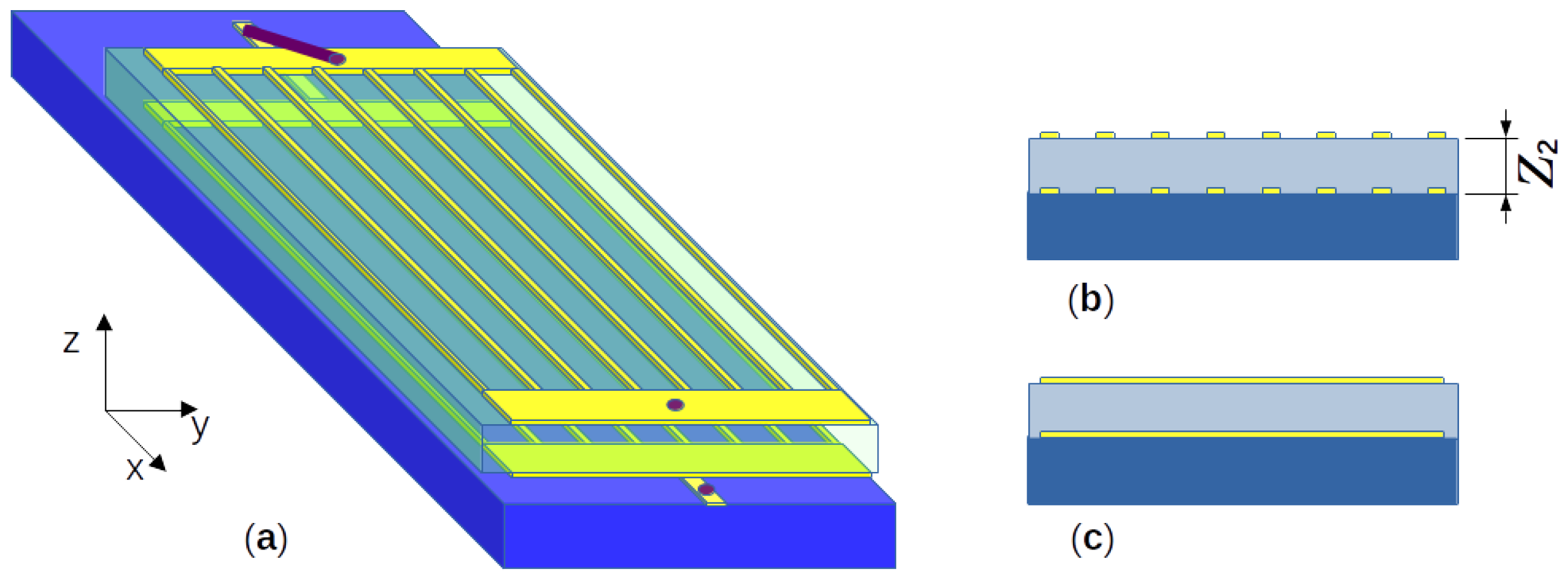
3. Model
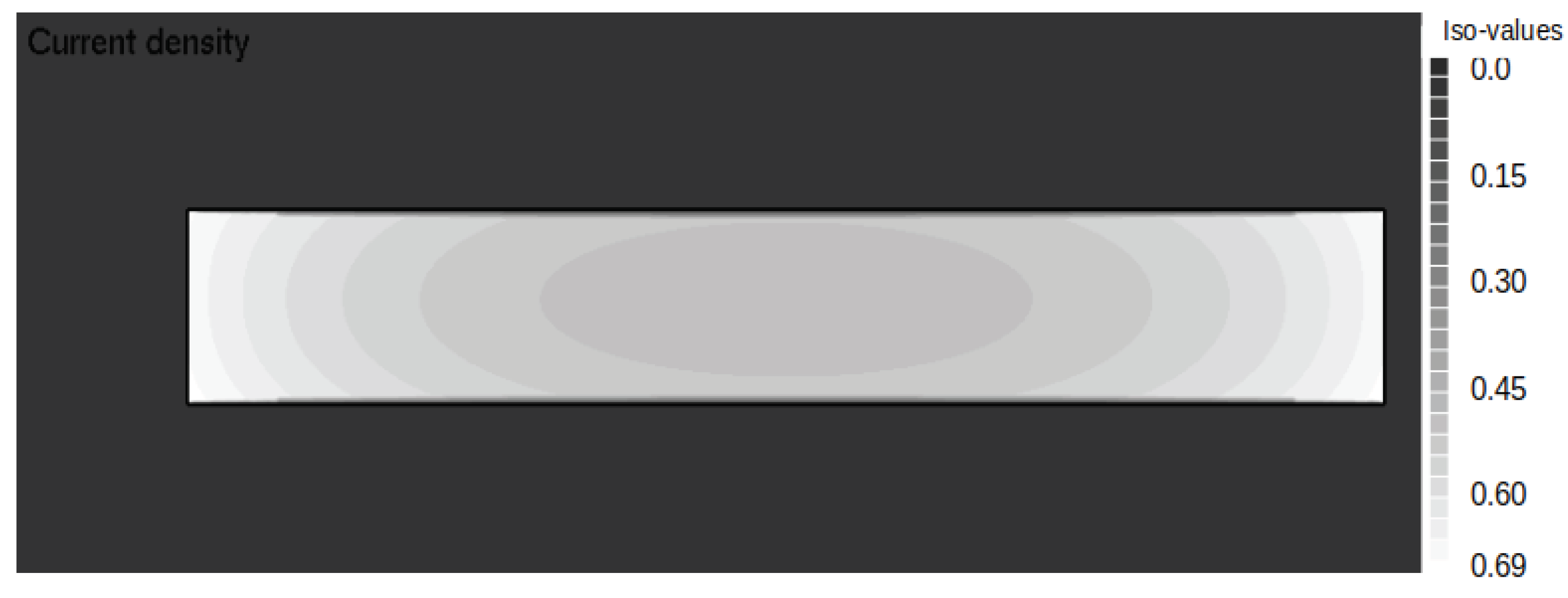
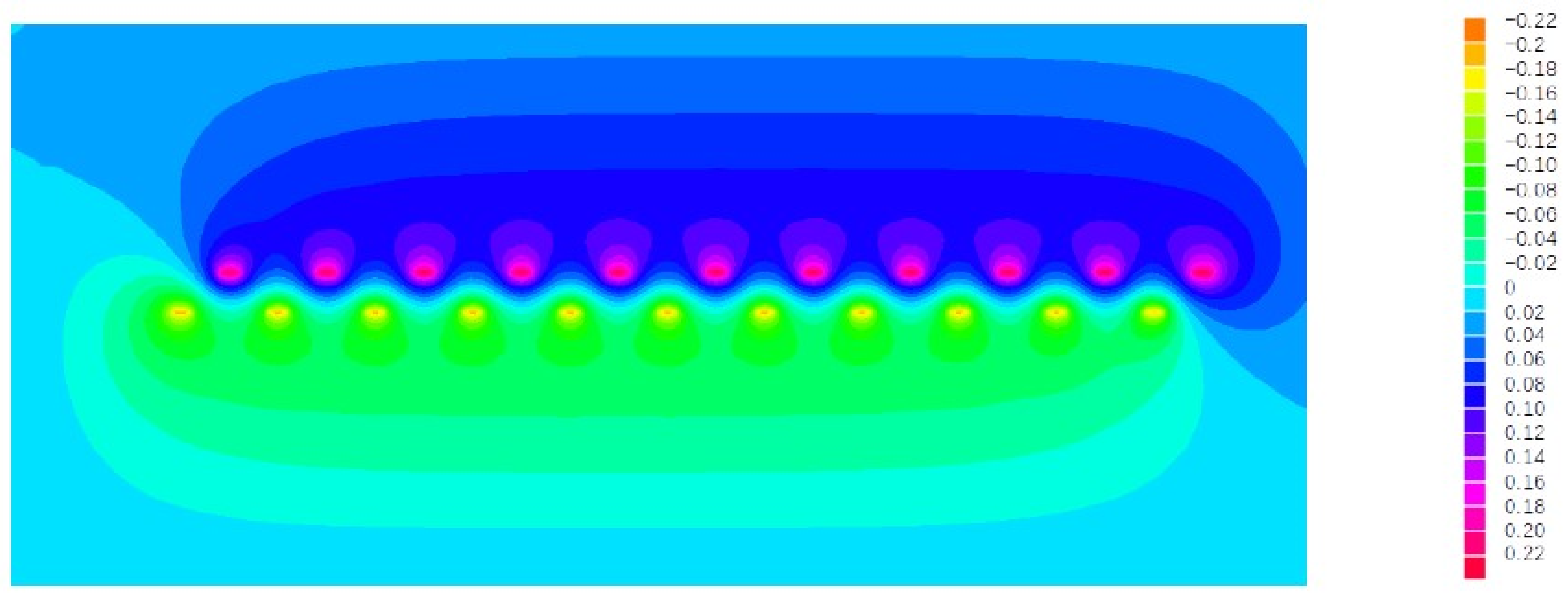
4. Results
4.1. Micrometer-Scale Circuits
4.2. Submicrometer-Scale Circuits
4.3. Dependence on Material Properties
5. Discussion
6. Conclusions
7. Patents
Author Contributions
Funding
Institutional Review Board Statement
Informed Consent Statement
Data Availability Statement
Conflicts of Interest
Abbreviations
| MDPI | Multidisciplinary Digital Publishing Institute |
| DOAJ | Directory of open access journals |
| JJ | Josephson junction |
| LJJ | Long Josephson junction |
References
- Clarke, J.; Braginski, A.I. (Eds.) The SQUID Handbook Vol. I: Fundamentals and Technology of SQUIDs and SQUID Systems; Wiley-VCH Verlag GmbH & Co. KgaA: Weinheim, Germany, 2004. [Google Scholar]
- Seidel, P. (Ed.) Applied Superconductivity: Handbook on Devices and Applications; Wiley: Weinheim, Germany, 2015. [Google Scholar]
- Clarke, J. Superconducting quantum interference devices for low frequency measurements. In Superconductor Applications: SQUIDs and Machines; Schwartz, B.B., Foner, S., Eds.; Plenum: New York, NY, USA, 1977. [Google Scholar]
- Vettoliere, A.; Silvestrini, P.; Granata, C. Superconducting quantum magnetic sensing. In Quantum Materials, Devices, and Applications; Henini, M., Oliveira Rodrigues, M., Eds.; Elsevier: Amsterdam, The Netherlands, 2023. [Google Scholar] [CrossRef]
- Cybart, S.A.; Herr, A.; Kornev, V.; Foley, C.P. Do multiple Josephson junctions make better devices? Supercond. Sci. Technol. 2017, 30, 090201. [Google Scholar] [CrossRef]
- Oppenländer, J.; Caputo, P.; Häussler, C.; Träuble, T.; Tomes, J.; Friesch, A.; Schopohl, N. Effects of magnetic field on two-dimensional superconducting quantum interference filters. Appl. Phys. Lett. 2003, 83, 969–971. [Google Scholar] [CrossRef]
- Drung, D.; Assmann, C.; Beyer, J.; Peters, M.; Ruede, F.; Schurig, T. DC SQUID Readout Electronics With Up to 100 MHz Closed-Loop Bandwidth. IEEE Trans. Appl. Supercond. 2005, 15, 777–780. [Google Scholar] [CrossRef]
- Kornev, V.K.; Kolotinskiy, N.V.; Skripka, V.A.; Sharafiev, A.V.; Mukhanov, O.A. Output power and loading of superconducting quantum array. IEEE Trans. Appl. Supercond. 2015, 25, 1602005. [Google Scholar] [CrossRef]
- Mitchell, E.E.; Müller, K.-H.; Purches, W.E.; Keenan, S.T.; Lewis, C.J.; Foley, C.P. Quantum interference effects in 1D parallel high-Tc SQUID arrays with finite inductance. Supercond. Sci. Technol. 2019, 32, 124002. [Google Scholar] [CrossRef]
- Oswald, D. Current and current density distribution in parallel superconducting wires in a planar array in the Meissner state. Cryogenics 1973, 13, 290–298. [Google Scholar] [CrossRef]
- Crété, D.; Lemaître, Y.; Marcilhac, B.; Trastoy, J.; Ulysse, C. Effect of self-induced flux in parallel arrays of Josephson junctions. In Proceedings of the IEEE International Superconductive Electronics Conference (ISEC), Riverside, CA, USA, 28 July–1 August 2019; pp. 1–3. [Google Scholar] [CrossRef]
- Barone, A.; Paternò, G. Physics and Applications of the Josephson Effect, 2nd ed.; J. Wiley & Sons: New York, NY, USA, 1982; Chapter 5. [Google Scholar]
- Weihnacht, M. Influence of Film Thickness on D.C. Josephson Current. Phys. Status Solidi B. 1969, 32, 169–172. [Google Scholar] [CrossRef]
- FreeFEM++. Available online: https://freefem.org/ (accessed on 23 May 2023).
- Alsop, L.E.; Goodman, A.S.; Gustavson, F.G.; Miranker, W.L. A Numerical Solution of a Model for a Superconductor Field Problem. J. Comput. Phys. 1979, 31, 216–239. [Google Scholar] [CrossRef]
- Khapaev, M.M.; Kupriyanov, M.Y.; Bakurskiy, S.V.; Klenov, N.V.; Soloviev, I.I. Modeling Superconducter SFN-Structures Using the Finite Element Method. Differ. Equat. 2020, 56, 959–967. [Google Scholar] [CrossRef]


| Aligned | Aligned | m | ||||
|---|---|---|---|---|---|---|
| Branch Nbr. | Upper Layer (%) | Lower Layer (%) | Upper Layer (%) | Lower Layer (%) | Upper Layer (%) | Lower Layer (%) |
| 1 | 14.2654 | −14.2654 | 9.05833 | −9.05837 | 9.03718 | −9.16116 |
| 2 | 14.2908 | −14.2908 | 9.09035 | −9.09033 | 9.08054 | −9.09618 |
| 3 | 14.2955 | −14.2955 | 9.09795 | −9.09793 | 9.08699 | −9.09087 |
| 4 | 14.2964 | −14.2964 | 9.10092 | −9.10092 | 9.08877 | −9.08988 |
| 5 | 14.2955 | −14.2955 | 9.10217 | −9.10218 | 9.08928 | −9.08975 |
| 6 | 14.2908 | −14.2908 | 9.10263 | −9.10261 | 9.08953 | −9.8949 |
| 7 | 14.2654 | −14.2654 | 9.10219 | −9.10220 | 9.08976 | −9.08934 |
| 8 | 9.10093 | −9.10088 | 9.08992 | −9.08879 | ||
| 9 | 9.09791 | −9.09792 | 9.09076 | −9.08695 | ||
| 10 | 9.0903 | −9.09032 | 9.09619 | −9.08045 | ||
| 11 | 9.05842 | −9.05843 | 9.16116 | −9.03722 | ||
| Branch Nbr. | Upper Layer (%) | Lower Layer (%) |
|---|---|---|
| 1 | 8.767 | −9.388 |
| 2 | 8.948 | −9.237 |
| 3 | 9.018 | −9.168 |
| 4 | 9.055 | −9.133 |
| 5 | 9.078 | −9.113 |
| 6 | 9.095 | −9.095 |
| 7 | 9.113 | −9.078 |
| 8 | 9.133 | −9.055 |
| 9 | 9.168 | −9.018 |
| 10 | 9.237 | −8.948 |
| 11 | 9.389 | −8.767 |
| m | m | |||
|---|---|---|---|---|
| Branch Nbr. | Upper Layer (%) | Lower Layer (%) | Upper Layer (%) | Lower Layer (%) |
| 1 | 9.03718 | −9.16116 | 8.93331 | −9.29025 |
| 2 | 9.08054 | −9.09618 | 9.05521 | −9.11825 |
| 3 | 9.08699 | −9.09087 | 9.07706 | −9.09461 |
| 4 | 9.08877 | −9.08988 | 9.08333 | −9.08884 |
| 5 | 9.08928 | −9.08975 | 9.08542 | −9.08744 |
| 6 | 9.08953 | −9.8949 | 9.08642 | −9.08638 |
| 7 | 9.08976 | −9.08934 | 9.08746 | −9.08556 |
| 8 | 9.08992 | −9.08879 | 9.08904 | −9.08339 |
| 9 | 9.09076 | −9.08695 | 9.09424 | −9.07695 |
| 10 | 9.09619 | −9.08045 | 9.11827 | −9.055 |
| 11 | 9.16116 | −9.03722 | 9.29025 | −8.93339 |
Disclaimer/Publisher’s Note: The statements, opinions and data contained in all publications are solely those of the individual author(s) and contributor(s) and not of MDPI and/or the editor(s). MDPI and/or the editor(s) disclaim responsibility for any injury to people or property resulting from any ideas, methods, instructions or products referred to in the content. |
© 2023 by the authors. Licensee MDPI, Basel, Switzerland. This article is an open access article distributed under the terms and conditions of the Creative Commons Attribution (CC BY) license (https://creativecommons.org/licenses/by/4.0/).
Share and Cite
Crété, D.G.; Menouni, S.; Trastoy, J.; Mesoraca, S.; Kermorvant, J.; Lemaître, Y.; Marcilhac, B.; Ulysse, C. Designing Large Two-Dimensional Arrays of Josephson Junctions for RF Magnetic Field Detection. Electronics 2023, 12, 3239. https://doi.org/10.3390/electronics12153239
Crété DG, Menouni S, Trastoy J, Mesoraca S, Kermorvant J, Lemaître Y, Marcilhac B, Ulysse C. Designing Large Two-Dimensional Arrays of Josephson Junctions for RF Magnetic Field Detection. Electronics. 2023; 12(15):3239. https://doi.org/10.3390/electronics12153239
Chicago/Turabian StyleCrété, Denis Gérard, Sarah Menouni, Juan Trastoy, Salvatore Mesoraca, Julien Kermorvant, Yves Lemaître, Bruno Marcilhac, and Christian Ulysse. 2023. "Designing Large Two-Dimensional Arrays of Josephson Junctions for RF Magnetic Field Detection" Electronics 12, no. 15: 3239. https://doi.org/10.3390/electronics12153239
APA StyleCrété, D. G., Menouni, S., Trastoy, J., Mesoraca, S., Kermorvant, J., Lemaître, Y., Marcilhac, B., & Ulysse, C. (2023). Designing Large Two-Dimensional Arrays of Josephson Junctions for RF Magnetic Field Detection. Electronics, 12(15), 3239. https://doi.org/10.3390/electronics12153239