Communication

A 3.7 GHz CPW Filtering Antenna with a Pair of Gain Zeros

1
School of Information Science and Engineering, Shandong University, Qingdao 266237, China
2
School of Microelectronics, Shandong University, Jinan 250100, China
3
School of Physical Science and Technology, Ningbo University, Ningbo 315211, China
4
Shanghai Convolution Communication Technology, Shanghai 201702, China
*
Author to whom correspondence should be addressed.
Electronics 2023, 12(9), 2145; https://doi.org/10.3390/electronics12092145
Submission received: 14 March 2023 / Revised: 4 May 2023 / Accepted: 4 May 2023 / Published: 8 May 2023

Abstract

:
In recent years, there has been a development of multifunctional components, including filtering antennas. Co-designing the filter and antenna can effectively reduce the overall size and thus realize high integration. A new coplanar waveguide (CPW) omnidirectional filtering antenna with a pair of gain zeros is presented using separation electric/magnetic coupling (SEMC) paths that greatly enhance frequency selectivity and effectively suppress the spurious responses of the circular patch radiator. The impedance bandwidth of the filtering antenna can also be controlled/adjusted through electric/magnetic coupling. The design results demonstrate that the filtering antenna achieves an omnidirectional pattern with a center frequency of 3.7 GHz, an impedance bandwidth of about 3%, a gain of 2.7 dBi, and a pair of gain zeros.

1. Introduction

In a wireless communication system, bandpass filters (BPFs) and antennas are essential and work together to receive and transmit the desired signals, while filtering undesired ones. With the fast development of 5G communication in recent years, there is a need to transmit and receive more information; however, as more and more data are transmitted at high rates, the channel space becomes very crowded, making the devices in adjacent working frequency bands easily coupled to each other such that the transmission signal quality of the communication system is lowered. In this context, low-cost filtering antennas [1,2,3,4,5,6,7,8,9,10,11] have received a lot of attention not only due to their increased requirement on mini-sized multi-purpose components, but also for their integration module that has filtering and radiating responses simultaneously, which improves circuit cooperativity.
Filtering antennas can be designed using several methods. The first method involves using a bandpass filter that is inserted into an antenna [1,10,12]. It is simple but easily introduces impedance mismatching between the antenna and the filter if the problem is ignored. The second method involves choosing the last resonator of a multi-resonator-coupled bandpass filter as the radiating element [4,5,6,7,8], which can be seen as a complex load of the bandpass filter. The third method involves using antenna filter-fusion technology [4,13], which can be realized by adding parasitic elements, digging defects, etc., in the circuit to generate gain zeros, while the filtering effect can be achieved without increasing the antenna size. Filtering antennas can also be designed using resonating slots in the feed line of antennas [14,15] using a DGS H filter for higher-order mode suppression [16] and a CPW feeding line [17]. Published studies have reported that most co-designed filtering antennas are composed of microstrip structures, with few reports on CPW antennas, and even where some designs use CPW feeding, the antenna radiators are still composed of microstrip structures. Meanwhile, many filters lack transmission zeros (TZs), which leads to the antenna gain having no gain zeros to improve the out-of-band suppression.
In this paper, a novel coplanar waveguide filtering antenna module with the integration of a highly selective coplanar waveguide bandpass filter and a double-sided circular patch radiator is proposed. The CPW bandpass filter generates dual controllable transmission zeros through the separation electric/magnetic coupling paths [18]. Electric coupling can be achieved by splitting a rectangular ring resonator, while magnetic coupling is achieved using the grounding stub; via holes that have the same effect in the microstrip structure are not needed, which reduces simulation time and manufacturing complexity. The integrated module not only effectively suppresses spurious responses—similar to the coplanar waveguide bandpass filter—but also has radiating responses similar to the circular-patch radiator. Simultaneously, the impedance bandwidth can be readily regulated by the electric and magnetic couplings. The proposed coplanar waveguide filtering antenna is also a candidate in millimeter-wave applications, and via holes are not needed, which facilitates fabrication.

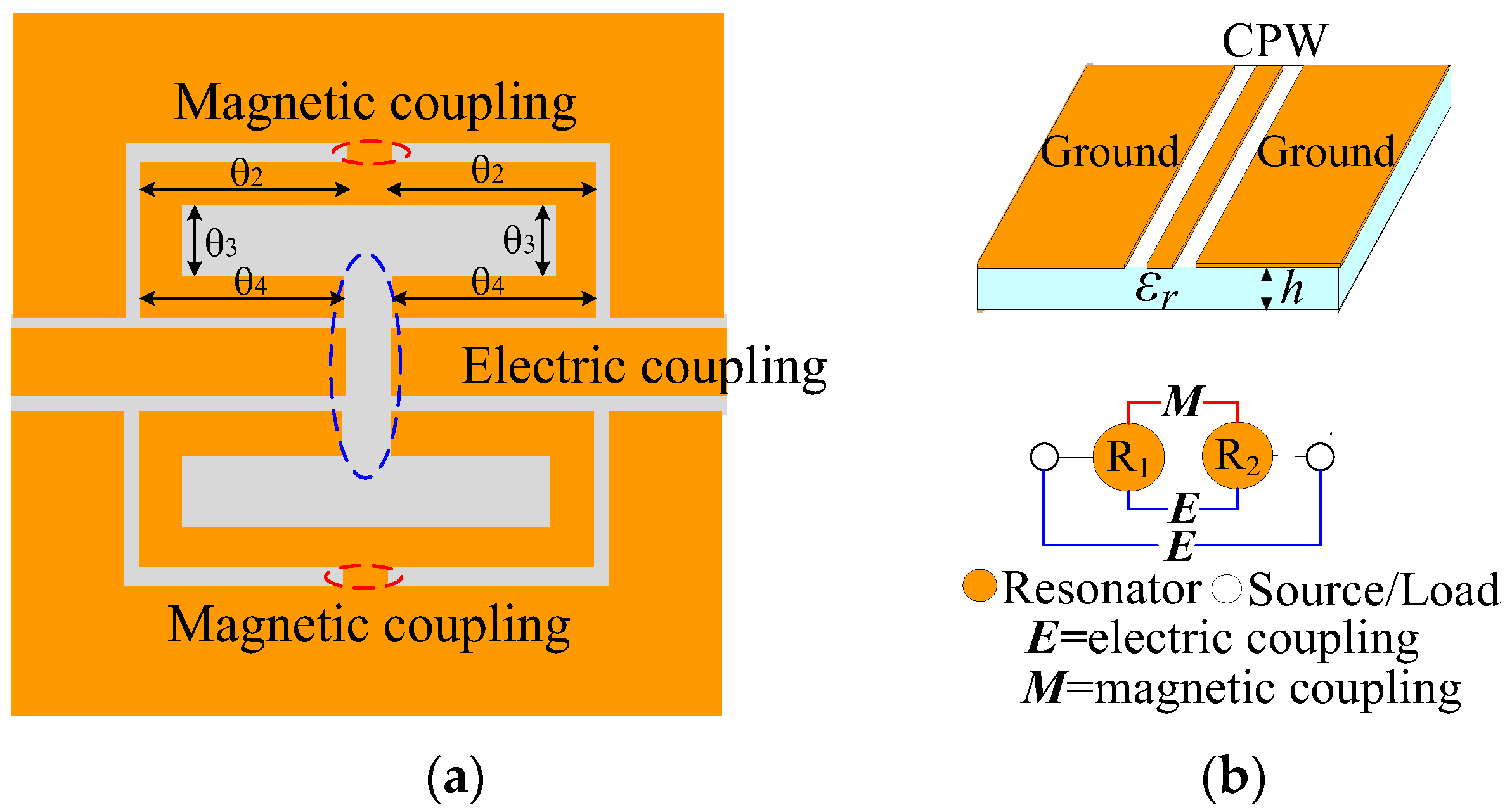
2. CPW Filtering Antenna Design

2.1. Structural Construction

The CPW filtering antenna is constructed with a coplanar waveguide bandpass filter and a double-sided circular radiator, as shown in Figure 1, where Figure 1a,b are the front view and the backside view of the filtering antenna, respectively. There is no transition structure between the filter and the radiator, which eliminates transition loss [4]. The CPW BPF consists of double capacitive coupled feeding lines and a second-order rectangular split ring uniform impedance resonator with separated electric and magnetic coupling paths [18], as shown in Figure 2, where Figure 2a is the filter topology and Figure 2b is the CPW structure and coupling structure. CPW has the advantages of easy shunt and series with the other components, and via holes are not required because the conductor strip and the ground are coplanar. On the other hand, CPW can be applied in a millimeter-wave frequency band. The ground shunt introduces magnetic coupling (M-coupling), while the rectangular split ring and the source load bring electric coupling (E-coupling). The M-dominant and the E-dominant coupling paths bring two transmission zeros. The circuit is designed on Rogers substrate, which has a relative dielectric constant of 2.2 and dielectric height of 0.508 mm.

2.2. Transmission Line Analysis

Figure 3a shows the equivalent transmission line (TL) circuit of the rectangular split ring uniform impedance resonator (UIR) with separation electric and magnetic coupling. Lc and Cc denote the coupling-inductance and coupling-capacitance of the split ring CPW UIR, respectively; Z1 is the impedance of the CPW uniform impedance resonator with a width of wu1. The corresponding electric length is shown in Figure 2. The equivalent circuit of the odd mode is provided in Figure 3b, and that of the even mode is provided in Figure 3c, where Z2 = Z3 = Z4 = Z1.
For the odd mode circuit in Figure 3b, coupling capacitance, Cm, is equivalentan to an open-circuited CPW transmission line. The electric length of the line can be represented as θ m = a r c t a n ( 2 Z 1 W o d C m ) . Electric length can be expressed as θ = w l ε r e / c , here l is the physical length, c is the velocity of light in free space, and ε r e is the effective permittivity. For the even mode circuit in Figure 3c, coupling inductance, Lm, is equivalent to a short-circuited CPW line, and the electric length of the transmission line can be derived as θ m = a r v t a n ( 2 Z 1 W o d L m ) , where W o d and W e v represent the resonant angular frequency of the odd mode and the even mode, respectively.
From the resonant mechanism of a resonator, resonance occurs when the input admittance of the odd mode and the even mode equals zero, that is , Y i n o = Y i n e = 0, thus the resonant conditions of the odd mode and the even mode can be obtained, respectively, as
2 ω o d C m [ Z 1 3 tan θ 4 ( 1 + tan θ 3 tan θ 2 ) + Z 1 3 ( tan θ 3 tan θ 2 ) ] + Z 1 2 ( tan θ 2 tan θ 3 1 ) + tan θ 4 ( Z 1 2 tan θ 2 + Z 1 2 tan θ 3 ) = 0
2 ω e v L m [ Z 1 2 ( tan θ 2 + tan θ 3 ) + tan θ 4 ( Z 1 2 Z 1 2 tan θ 2 tan θ 3 ) ] + Z 1 3 ( tan θ 2 tan θ 3 1 ) + Z 1 3 tan θ 4 ( tan θ 2 + tan θ 3 ) = 0
The 2-order CPW bandpass filter is designed with a center frequency of 3.7 GHz and a fractional bandwidth (FBW) of 3.2%. The element values of the low-pass prototype can be obtained as g0 = 1, g1 = 0.4683, g2 = 0.4219 and g3 = 1.0533. According to Qe1 = g0g1/FBW, Qen = gngn + 1/FBW, the input and output external quality factors can be calculated as Qei = 14.63 and Qeo = 13.89.

3. Design Analysis and Results of the CPW Filtering Antenna

The filtering antenna is designed to center at 3.7 GHz, with an impedance bandwidth of 3%. The filtering antenna dimensions are obtained by identifying the substrate and resonant conditions in (1) and (2) and then optimized using full-wave EM simulator HFSS, as listed in Table 1. For certain dimensions, the resonance simulated by HFSS for the rectangular split ring UIR with separate electric/magnetic coupling approaches can be calculation from (1) and (2). The circular patch radiator has the same central frequency as the CPW bandpass filter.

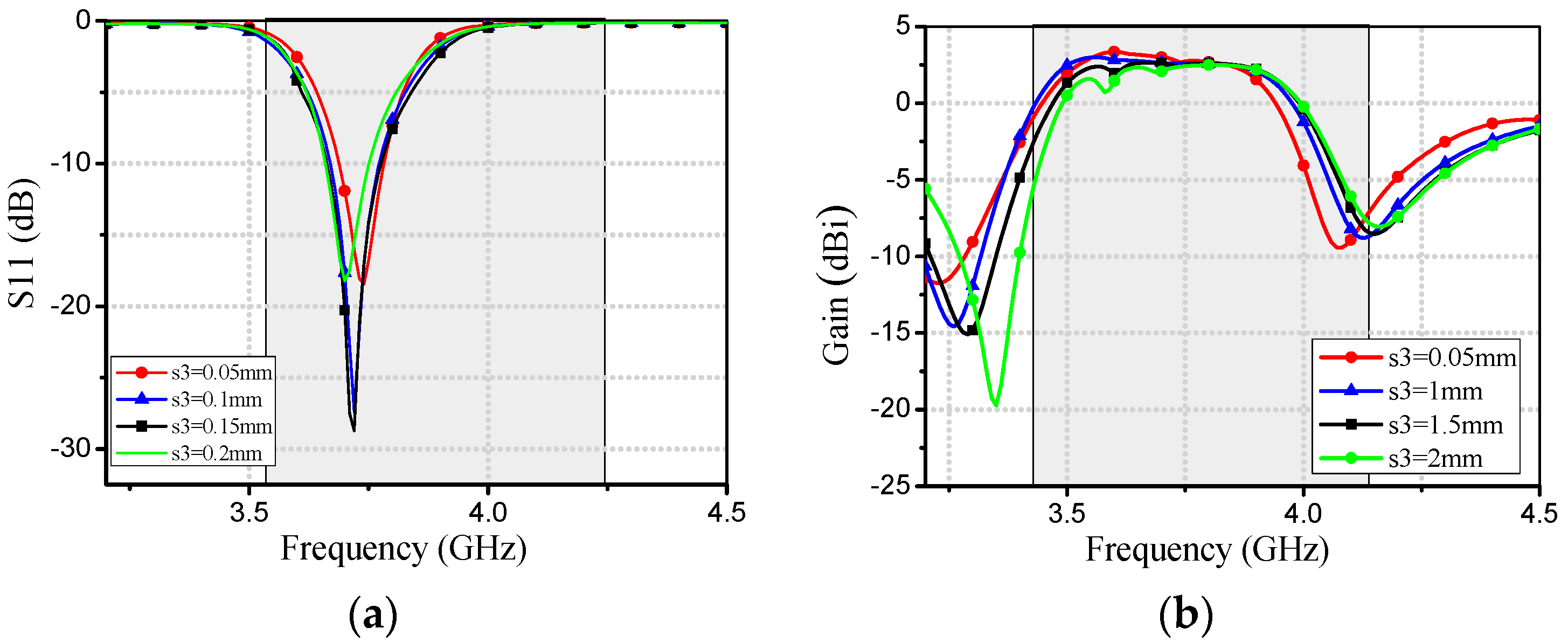
3.1. S-Parameter and Gain of the CPW Filtering Antenna

Simulation filtering antenna frequency responses for the dimensions provided above are shown in Figure 4. Figure 4a shows that the filtering antenna works at 3.7 GHz and the S11 attenuation is no more than 26 dB. Figure 4b shows that the filtering antenna has gain of more than 2.5 dBi, from 3.5 GHz to 3.84 GHz, and dual gain zeros are realized at 3.25 GHz and 4.12 GHz. The gain zeros are due to the filter transmission zeros, which are produced by the 2-order split ring UIR with SEMC.
The uniform resonator shown in Figure 2a generates electric and magnetic coupling, where the electric field is main on the split, labelled as electric coupling, and magnetic field is main on the grounded stub, labelled as magnetic coupling. The split width s3 and stub width wu2 versus filtering antenna frequency responses are discussed, as shown in Figure 5 and Figure 6, respectively.
The effects of electric coupling on S-parameter and gain are shown in Figure 5a and b, respectively. As s3 increases gradually, the attenuation of S11 first decreases and then increases, and when s3 = 0.1 mm, the antenna achieves favorable return loss and impedance matching, as shown in Figure 5a. As for gain versus s3, when s3 changes from 0.05 mm to 2 mm, the attenuation of the gain zero on the left side increases, thus enhancing the out-of-band suppression level. However, the attenuation of the right gain zero decreases with increasing s3, leading to a lowering of the out-of-band suppression level. Additionally, the gain in the passband is significantly reduced when s3 equals 1.5 mm or 2 mm, and the filtering antenna has a better gain when s3 = 1 mm.
The effect of magnetic coupling on S-parameter and gain are shown in Figure 6a and b, respectively. As wu2 gradually increases, the attenuation of S11 first decreases and then increases, while the antenna’s working frequency simultaneously increases. The antenna achieves the best impedance matching when wu2 = 1.5 mm, as shown in Figure 6a. As for the antenna gain, when wu2 changes from 1 mm to 2.5 mm, attenuation of the gain zero on the left side decreases and the out-of-band suppression level reduces, while attenuation of the right gain zero remains nearly unchanged, although the zero shifts to a higher frequency. The filtering antenna has favorable gain when wu2 = 1.5 mm. Figure 5 and Figure 6 demonstrate that filtering antenna matching and gain zeros can be adjusted through electromagnetic couplings.
As a comparison, simulated S-parameter and gain of the antenna (the filter is removed from the filtering-antenna structure) are shown in Figure 7. The figure shows that there is out-of-band spurious and discontinuity of gain, but there is no gain zero without the filtering part. Antenna performance can be improved when the filter is introduced, as shown in Figure 7.

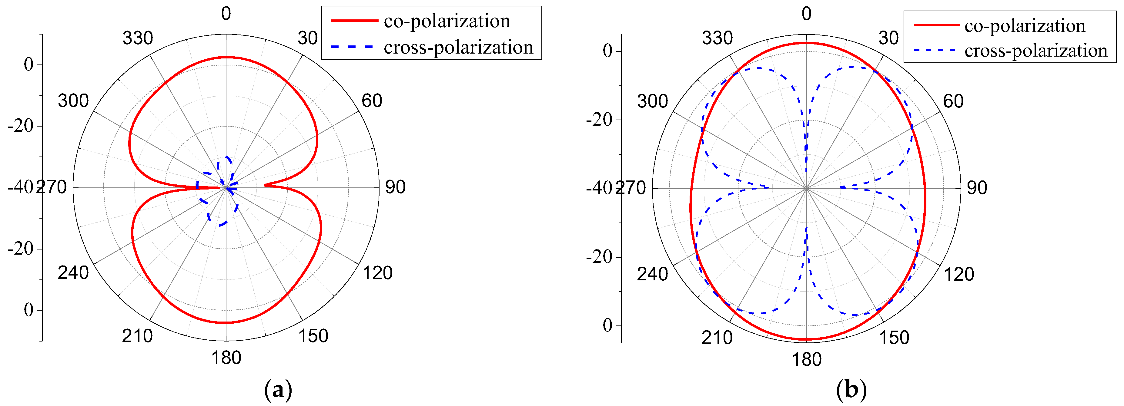
3.2. Patterns and Current Profile of the CPW Filtering Antenna

A simulated filtering antenna surface current profile is provided in Figure 8. The current is predominantly distributed around the CPW resonator with electric and magnetic couplings and the circular patch radiator, and the currents run through the circular-patch radiator without altering the orientation. This shows that the filtering antenna can generate a nearly omnidirectional pattern in the plane that is parallel to the magnetic field. Antenna radiation is closely connected to the antenna surface current.
The simulated co-/cross-polarization patterns of the CPW filtering antenna and the antenna without the filtering part are shown in Figure 9 and Figure 10. The E-plane and the H-plane of the co-/cross-polarization patterns of the CPW filtering antenna are shown in Figure 9a and b, respectively, while the E/H planes of the CPW antenna without the filtering part are shown in Figure 10a and b, respectively. The antennas with and without filtering parts have similar radiation patterns and it can be concluded that our proposed filter with SEMC has almost no influence on antenna patterns, although it helps to improve out-of-band suppression and gain discontinuity.

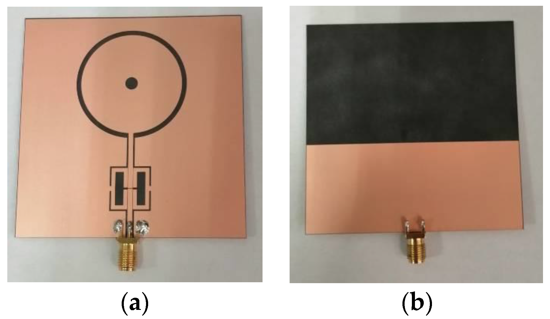
3.3. Fabrication and Experimental Results

The proposed CPW filtering antenna is manufactured as shown in Figure 11a,b. Measured results of S-parameter and gain of the filtering antenna are shown in Figure 12a,b. Measured filtering antenna patterns for E/H planes are shown in Figure 13a and b, respectively. The measured results are similar to the simulations. The filtering antenna had measured impedance bandwidth of about 3% and maximum gain of 2.98 dBi, and gain zeros and omnidirectional radiation were verified. The error between measurement and simulation results may be due to fabrication uncertainty and material errors.

3.4. Performance Comparisons

Differences between this study and relevant published reports are given in Table 2. The presented filtering antenna has higher working frequency than reported in the literature [4,8,11], has more gain zeros than reported in [4,5,8,19,20,21], and more gain than reported in [4,8,20,21]. It also has better out-band rejection compared with references [4,5,8,11]. Meanwhile, the CPW structure is not commonly used. The advantages of controllable bandwidth, gain zeros, and small circuit dimension have been verified.

4. Conclusions

A new coplanar waveguide filtering antenna that utilizes double 2-order rectangular-shaped split-ring resonators with SEMC and a CPW circular radiator is presented. The filtering antenna was analyzed and the measured results agree with the simulation, which has a center frequency of 3.7 GHz, a radiation gain of about 2.98 dBi, and an impedance bandwidth of about 3% with a S11 attenuation of more than 12 dB. The new integration design of the filtering antenna not only has radiation patterns similar to those of the circular radiator, but also generates a pair of gain zeros that effectively suppress undesired spurious responses. The gain zeros enhance frequency selectivity through electromagnetic coupling of the filter section, while the antenna bandwidth can also be controlled by the electromagnetic couplings. The proposed CPW filtering antenna has a simple topology, and transition circuit and via holes are not required, thus reducing the cost of design and manufacture. Thus, it has potential development on dual-band and applications in millimeter wave bands.

Author Contributions

Conceptualization, Y.D. and Y.X.; methodology, Y.D., W.H. and R.Y.; software, Y.D. and J.X.; validation, P.W. and Y.X.; formal analysis, Y.D. and R.Y.; investigation, P.W., R.Y. and Y.X.; resources, J.X.; writing—original draft preparation, Y.D. and J.X.; writing—review and editing, Y.D., Y.X., W.H. and R.Y.; supervision, J.X. and P.W.; project administration, J.X. All authors have read and agreed to the published version of the manuscript.

Funding

This research was funded by the Beidou New Time-space Intelligent Industry Development Collaborative Innovation Center (grant number 2021YFB1407001).

Informed Consent Statement

Not applicable.

Data Availability Statement

The data used to support the findings of this study are available from the corresponding author upon request.

Conflicts of Interest

The authors declare that they have no conflict of interest.

References

  1. Chu, H.; Jin, C.; Chen, J.X.; Guo, Y.X. A 3-D millimeter-wave filtering antenna with high selectivity and low cross-polarization. IEEE Trans. Antennas Propag. 2015, 63, 2375–2380. [Google Scholar] [CrossRef]
  2. Hu, H.; Chen, F.; Chu, Q. Novel Broadband Filtering Slotline Antennas Excited by Multimode Resonators. IEEE Antennas Wirel. Propag. Lett. 2017, 16, 489–492. [Google Scholar] [CrossRef]
  3. Zhang, Y.; Zhang, X.; Pan, Y. Compact Single- and Dual-Band Filtering Patch Antenna Arrays Using Novel Feeding Scheme. IEEE Trans. Antennas Propag. 2017, 65, 4057–4066. [Google Scholar] [CrossRef]
  4. Wu, W.J.; Yin, Y.Z.; Zuo, S.L.; Zhang, Z.Y.; Xie, J.J. A New Compact Filter-Antenna for Modern Wireless Communication Systems. IEEE Antennas Wirel. Propag. Lett. 2011, 10, 1131–1134. [Google Scholar]
  5. Zuo, J.; Chen, X.; Han, G.; Li, L.; Zhang, W. An integrated approach to RF antenna-filter co-design. IEEE Antennas Wirel. Propag. Lett. 2009, 8, 141–144. [Google Scholar]
  6. Chen, Y.; Hong, W.; Kuai, Z.; Wang, H. Ku-band linearly polarized omnidirectional planar filtenna. IEEE Antennas Wirel. Propag. Lett. 2012, 11, 310–313. [Google Scholar] [CrossRef]
  7. Mao, C.-X.; Gao, S.; Wang, Y.; Qin, F.; Chu, Q.-X. Multimode resonator-fed dual-polarized antenna array with enhanced bandwidth and selectivity. IEEE Trans. Antennas Propag. 2015, 63, 5492–5499. [Google Scholar] [CrossRef]
  8. Chuang, C.-T.; Chung, S.-J. Synthesis and design of a new printed filtering antenna. IEEE Trans. Antennas Propag. 2011, 59, 1036–1042. [Google Scholar] [CrossRef]
  9. Atallah, H.A.; Abdel-Rahman, A.B.; Yoshitomi, K.; Pokharel, R.K. CPW-Fed UWB antenna with sharp and high rejection multiple notched bands using stub loaded meander line resonator. Int. J. Electron. Commun. (AEÜ) 2018, 83, 22–31. [Google Scholar] [CrossRef]
  10. Prashant, R.J.; Saurabh, R.J.; Gaurav, U.; Shivesh, T.; Vijay, S.T. Circularly slotted flower shaped UWB filtering antenna with high peak gain performance. Int. J. Electron. Commun. (AEÜ) 2017, 81, 209–217. [Google Scholar]
  11. Sung, Y.J. Microstrip Resonator Doubling as a Filter and as an Antenna. IEEE Antennas Wirel. Propag. Lett. 2010, 9, 467–470. [Google Scholar] [CrossRef]
  12. Cahyasiwi, D.A.; Rahardjo, E.T. Circular Patch Filtering Antenna Design Based on Hairpin Bandpass Filter. In Proceedings of the 2018 International Symposium on Antennas and Propagation (ISAP), Busan, Republic of Korea, 23–26 October 2018; pp. 1–2. [Google Scholar]
  13. Chen, C. A Compact Wideband Endfire Filtering Antenna Inspired by a Uniplanar Microstrip Antenna. IEEE Antennas Wirel. Propag. Lett. 2022, 21, 853–857. [Google Scholar] [CrossRef]
  14. Al-Nuaimi, M.K.T.; Whittow, W.G. Compact microstrip bandstop filter using SRR and CSSR Design, simulation, and results. In Proceedings of the Fourth European Conference on Antennas and Propagation, Barcelona, Spain, 12–16 April 2010. [Google Scholar]
  15. Yahya, L.S.; Sayidmarie, K.H.; Elmegri, F.; Abd-Alhameed, R.A. Crescent-shaped double-monopole antennas with reduced coupling for WLAN and WIMAX applications. In Proceedings of the Internet Technologies and Applications (ITA), Wrexham, UK, 8–11 September 2015. [Google Scholar] [CrossRef]
  16. De Souza, F.A.A.; Campos, A.L.P.D.S.; Neto, A.G.; Serres, A.J.R.; De Albuquerque, C.C.R. Higher Order Mode Attenuation in Microstrip Patch Antenna with DGS H Filter Specification from 5 to 10 GHz Range. J. Microwaves. Optoelectron. Electromagn. Appl. 2020, 19, 214–227. [Google Scholar] [CrossRef]
  17. Wang, C.; Wang, L.; Zhang, Y.; Hu, W.; Jiang, X. A Filtering Dielectric Resonator Antenna Using CPW Fed for Sub-6GHz Applications. Proaress Electromagn. Res. Lett. 2022, 105, 49–56. [Google Scholar] [CrossRef]
  18. Ma, K.X.; Ma, J.G.; Yeo, K. A compact size coupling controllable filter with separate electric and magnetic coupling paths. IEEE Trans. Microw. Theory Tech. 2006, 54, 1113–1119. [Google Scholar]
  19. Al-Arajee, T.H.; Sayidmarie, K.H. A Circular Monopole Filtenna with Inverted L-shaped Stub for 5G Applications. Int. J. Microw. Opt. Technol. 2021, 16, 608–617. [Google Scholar]
  20. Al-Arajee, T.H.; Sayidmarie, K.H. A Rectangular Monopole Filtenna with U-shaped Slot for 5G Applications. In IOP Conference Series: Materials Science and Engineering; IOP Publishing: Bristol, UK, 2021; Available online: https://iopscience.iop.org/article/10.1088/1757-899X/1152/1/012011/meta (accessed on 10 January 2023).
  21. Juma’a, F.K.; Al-Mayoof, A.I.; Abdulhameed, A.A.; Alnahwi, F.M.; Al-Yasir, Y.I.A.; Abd-Alhameed, R.A. Design and Implementation of a Miniaturized Filtering Antenna for 5G Mid-Band Applications. Electronics 2022, 11, 2979. [Google Scholar] [CrossRef]
Figure 1. The proposed CPW filtering antenna. (a) Top view, (b) Back side view.
Electronics 12 02145 g001
Figure 2. Bandpass filter section. (a) Bandpass filter topology. (b) CPW and the filter coupling structure.
Electronics 12 02145 g002
Figure 3. Equivalent TL model of the 2-order split ring CPW resonator with SEMC. (a) Total equivalent TL circuit. (b) Circuit of the odd mode. (c) Circuit of the even mode.
Electronics 12 02145 g003
Figure 4. Filtering antenna S-parameter and gain. (a) Simulated S11. (b) Simulated antenna gain.
Electronics 12 02145 g004
Figure 5. S11 and gain of the filtering antenna versus parameter s3. (a) S11 versus s3. (b) Filtering antenna gain versus parameter s3.
Electronics 12 02145 g005
Figure 6. S11 and gain of the filtering antenna versus parameter wu2. (a) S11 versus wu2. (b) Gain versus wu2.
Electronics 12 02145 g006
Figure 7. S-parameter and gain of the antenna (when the filter is removed). (a) S11. (b) Gain.
Electronics 12 02145 g007
Figure 8. Surface current distribution of the CPW filtering antenna at 3.7 GHz.
Electronics 12 02145 g008
Figure 9. Filtering antenna patterns at 3.7 GHz. (a) E-plane (xoz). (b) H-plane (yoz).
Electronics 12 02145 g009
Figure 10. Antenna patterns (filter part is removed). (a) E-plane (xoz). (b) H-plane (yoz).
Electronics 12 02145 g010
Figure 11. Manufactured filtering antenna. (a) Top view. (b) Backside view.
Electronics 12 02145 g011
Figure 12. Measured results of S-parameter and gain. (a) Measured S11. (b) Measured gain.
Electronics 12 02145 g012
Figure 13. Measured filtering antenna patterns. (a) E-plane (xoz) pattern. (b) H-plane (yoz) pattern.
Electronics 12 02145 g013
Table 1. Dimensions of the proposed filtering antenna (mm).
WLw1g1wu1wu2lu1
70701.50.51.21.512.2
lu2s1s2s3r1r2w2
12.20.20.10.2161929
Table 2. Contrast between our study and previously published studies.
ReferencesCenter Frequency
(GHz)
Gain ZerosSpurious ResponsesBandwidth
Controllable
Max. Gain
(dBi)
Circuit TypeSize
(mm2)
[4]2.45nonona2.41microstrip43 × 30
[5]3.95noyesna4.3microstrip30 × 20
[8]2.45nonona−1.3microstrip60 × 70
[11]0.672yesna4.2microstrip80 × 80
[19]
double stub
3.6noyes-3.13microstrip35 × 44
[20]3.6noyes-2.57microstrip35 × 44
[21]3.68nono-2.2microstrip24.2 × 27
This work3.72noyes2.98CPW70 × 70
Disclaimer/Publisher’s Note: The statements, opinions and data contained in all publications are solely those of the individual author(s) and contributor(s) and not of MDPI and/or the editor(s). MDPI and/or the editor(s) disclaim responsibility for any injury to people or property resulting from any ideas, methods, instructions or products referred to in the content.

