Article

Digital Finite Impulse Response Equalizer for Nonlinear Frequency Response Compensation in Wireless Communication

1
Department of Electrical and Computer Engineering, University of Alberta, Edmonton, AB T6G 2R3, Canada
2
Department of Electronics and Information Engineering, Beijing-Dublin International College, Beijing University of Technology, Beijing 100022, China
*
Author to whom correspondence should be addressed.
Electronics 2023, 12(9), 2010; https://doi.org/10.3390/electronics12092010
Submission received: 25 March 2023 / Revised: 23 April 2023 / Accepted: 25 April 2023 / Published: 26 April 2023
(This article belongs to the Special Issue Advanced Design of RF/Microwave Circuit)

Abstract

:
Signal distortion can occur when the gain or attenuation of a component changes non-linearly with frequency, which is referred to as nonlinear frequency response. Common communications components such as filters, amplifiers, and mixers can lead to nonlinear frequency responses, which can cause errors in transmitting and receiving. This article outlines the design and demonstration of a static and dynamic finite impulse response (FIR) digital equalizer circuit. Using predistortion topology with a coupled feedback loop, the adaptive Least-Mean Square (LMS) algorithm was implemented. The FIR filter was simulated in MATLAB and Vivado and then implemented onto an Eclypse Z7 Field Programmable Gate Array (FPGA) evaluation board. Simulations showed that the custom RTL module gave the same frequency response that was produced in MATLAB calculations. The filter was able to dynamically equalize the frequency responses of different nonlinear boards that were used as the devices under test (DUT). Measurements showed that the equalizer was able to compensate for system distortion from 0.2 to 0.8 Nyquist frequency. The phase response remained relatively linear across the band of interest, with a group delay flatness less than 10 ns.

1. Introduction

Radio frequency (RF) signals transmitted over long distances typically have RF interference and lose power in their signals, which is largely determined by path lengths, path angles, and medium attenuation factors [1,2,3]. This affects signals in many technologies in wireless communications, from Bluetooth and WLAN to earth-satellite radio-paths and radio detection of cosmic rays [4,5]. To compensate for the attenuation and RF interference, improved transmitter and receiver antennas, analog filters, amplifiers, and mixers are implemented [6]. For example, low noise amplifiers (LNAs) are typically implemented in receiver front-ends to decrease the noise figure (to the limiting thermal noise of the FETs) of the low power input signals, however often these components have large phase and amplitude response errors in their frequency response [7,8,9], compounding with other frequency response errors in the RF transmission path from passive and active devices. Although improvements to flatten the frequency response could be made with analog devices easily implemented in the RF path, digital filters can be much more versatile and adaptive [6,10,11].
In a non-adaptive scenario, the coefficients of finite impulse response (FIR) filter must be determined before processing the signal. In an adaptive FIR filter, the coefficients are continuously “adapted to minimize the error signal” [11]. Adaptive equalization techniques in digital communication systems date back to the 1960s [12]. Since then, a large number of research articles have been devoted to this field [13,14,15,16,17]. However, these literatures either required a training sequence and assumed little variation of the transmission channel over time, or implemented blind adaptation algorithms that are best suited for specific modulation schemes [18]. At the same time, almost all these articles only evaluated their circuit performance in the time domain.
This paper presents an innovative digital equalizer with excellent frequency response. The novelty of this work lies in the implementation of adaptive equalization in RF front-ends using a novel approach. Although pre- and post-distortion techniques have been used before in power amplifier designs, this work proposes a new equalization technique that has not been explored before. Specifically, the equalization technique proposed in this work utilizes the concept of FIR filters without actually designing a “true” standard FIR filter. Instead, the FIR coefficients are obtained through real-time S-parameter measurements of the device under test (DUT). This approach is unique and has not been reported in the literature. Therefore, the contribution of this work is a novel adaptive equalization technique that can be used to improve the performance of RF front-ends in communication systems. To demonstrate our proposed technique, static and dynamically configured digital equalization was implemented for DUT which in our case consists of a self-made nonlinear circuit board cascaded with a commercial off-the-shelf RF amplifier (ZHL-6A+ from Mini-Circuits), to mimic the nonlinear frequency response of a wireless communication system. Our circuit can be placed in the transmitter before the digital-to-analog converter (DAC) or in the receiver after the analog-to-digital converter (ADC), as illustrated in Figure 1a,b. Using high-speed ADCs and DACs, our proposed structure can also be deployed in the RF path for nonlinear compensation.

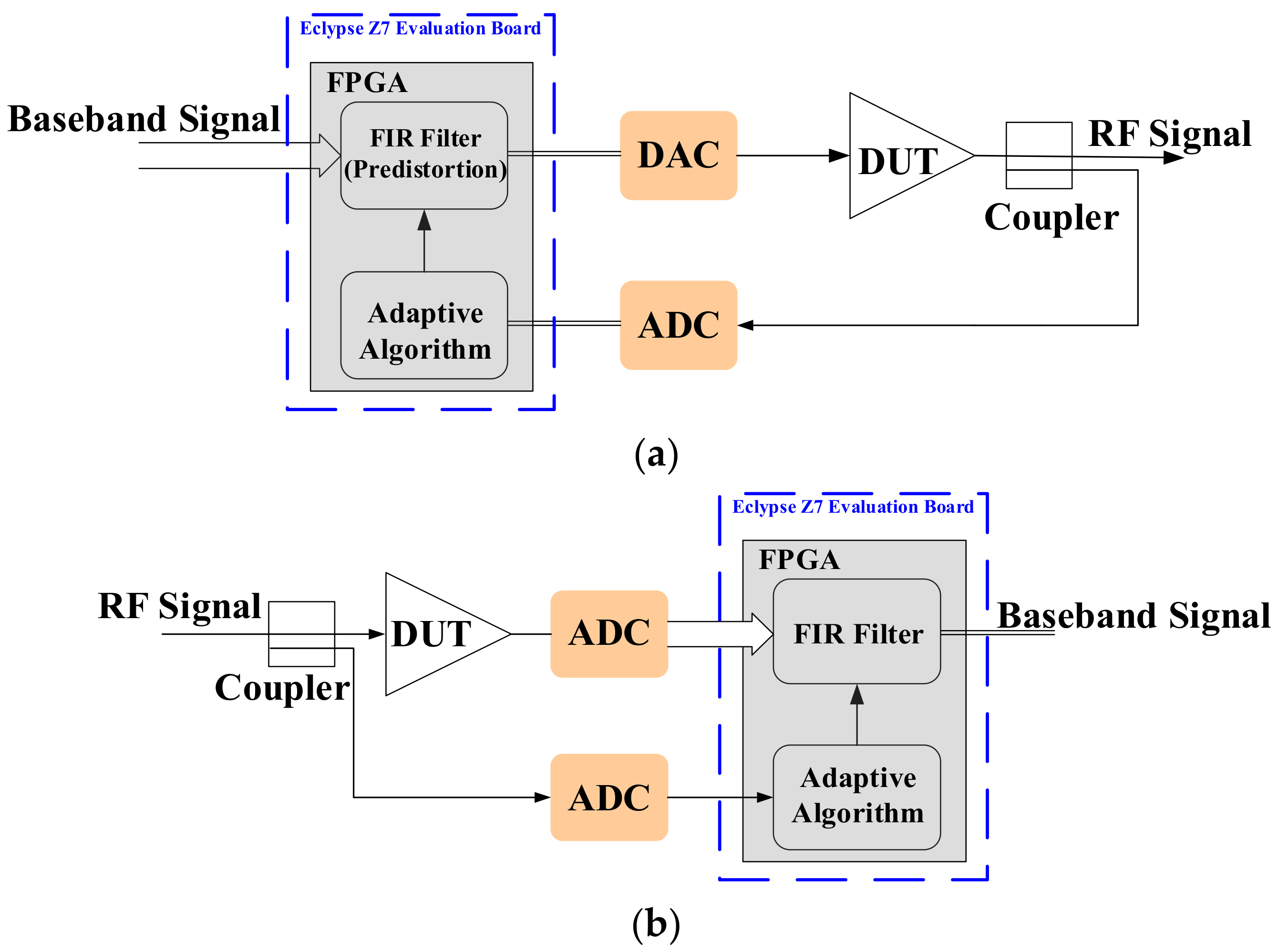
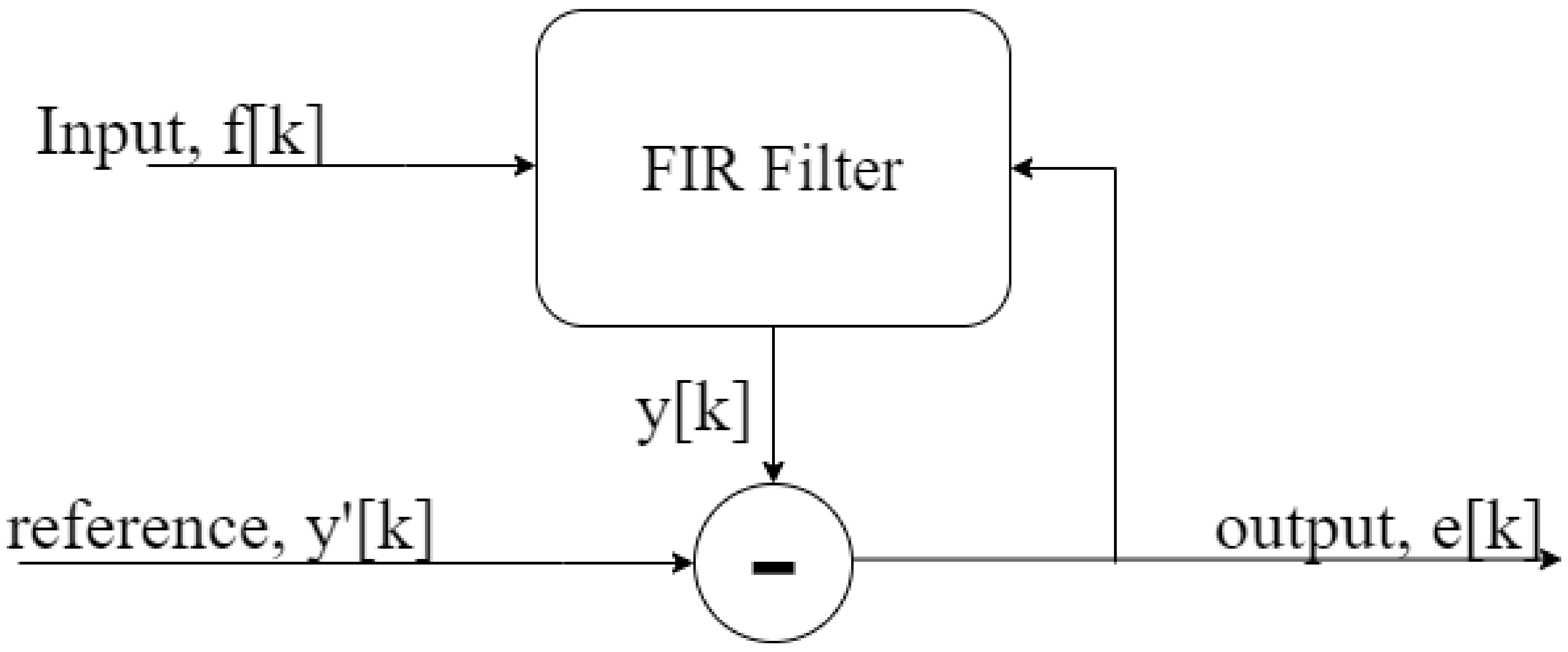
2. Principle of Digital Predistortion Equalizer Realized by Adaptive Algorithm

2.1. Equalizer Topology

In our design, the adaptive feature is achieved by introducing a closed loop for error correction. Our proposed device can locate before the DAC in the transmitting path or after the ADC in the receiving path. For example, in the uplink, the modulated baseband signal travels through the FIR filter first for predistortion, then through the DUT and then the RF feedback is taken through a coupler to the Field Programmable Gate Array (FPGA) for comparison. Error information is then generated to update the FIR filter coefficients. This process is illustrated in the simplified block diagram in Figure 1a.
For a digital FIR filter with N taps and order N 1 , the output is found by:
y [ k ] = n = 0 N 1 b k [ n ] f [ k n ]
where k is the sample time, y [ k ] is the output, b k is the coefficient of tap n at time k , and f [ k ] is the input [10]. The FIR filter is causal, and finite since the impulse response is given by (2). In a non-adaptive, b k [ n ] must be determined before processing the signal.
h [ k ] = n = 0 N 1 b n δ [ k n ] = b k 0 < n < N 1 0 o t h e r w i s e
Now, the FPGA has a reference to reduce the error through the adaptive algorithm using Least-Mean Square (LMS) as described in (3) to determine the new coefficients.
b k + 1 [ n ] = b k [ n ] + K · e [ k ] · f [ k n ]
where e [ k ] is the error signal between the target y [ k ] and the output y [ k ] , and K is the rate of adaptation [11]. A general block diagram of this adaptive method is illustrated in Figure 2.

2.2. LMS Coefficients Derivation

There are several methods for determining the coefficients to an N-tap FIR Filter as outlined by Proakis [19]. The most straightforward method is by directly taking the inverse discrete Fourier transform (IFT). For an absolutely summable Bounded-Input Bounded-Output (BIBO) frequency response given by a real and imaginary value, the coefficients can be found directly by taking the Fourier transform of either the real or imaginary components. A better method that requires no guesswork is to find the desired frequency response using Least Mean Squares to solve the system of equations, which can also be weighted, similar to in low-pass and high-pass FIR filters where the passband is given a higher weight. An FIR filter of order N 1 (length N ), the frequency response is:
H ( ω ) = n = 0 N 1 b n e i ω n
Here, ω = 2 π f / f s is the normalized frequency from DC to Nyquist. If the frequency response is discretized with frequencies ω 0 , ω 1 , ω 2 , ω M 1 then the matrix equivalent for an M-point frequency response H ( ω M ) is given by (5)
H ( ω 0 ) H ( ω 1 ) H ( ω M 2 ) H ( ω M 1 ) = 1 e i ω 0 e i ω 0 ( N 2 ) e i ω 0 ( N 1 ) 1 e i ω 1 e i ω 1 ( N 2 ) e i ω 1 ( N 1 ) 1 e i ω M 2 e i ω M 2 ( N 2 ) e i ω M 2 ( N 1 ) 1 e i ω M 1 e i ω M 1 ( N 2 ) e i ω M 1 ( N 1 ) b 0 b 1 b N 2 b N 1
Let the matrix be labeled as A and the LHS and RHS vectors be labelled as H and b respectively. A requirement is that the coefficients b are real, that is, A C M × N and H C M × 1 and b R N × 1 . Since this is an absolutely summable system, the real and imaginary components can be taken independently by extending the matrix resulting in real components only, such as:
R ( H ) I ( H ) = R ( A ) I ( A ) b
Now, the new vector to the LHS and matrix on the RHS can be labelled as H e x t and A e x t , respectively. In other words, the complex H = A b becomes H e x t = A e x t b e x t . Furthermore, A e x t R 2 M × N and H e x t R 2 M × 1 and the entire system of equations is in the real domain [20]. Now, given a desired frequency response D e x t , the LMS algorithm can be applied to the equation:
D e x t = A e x t b
The solution to the LMS problem is given by:
b = A e x t T A e x t 1 A e x t T D e x t
which minimizes:
error = D e x t A e x t b
Furthermore, improvements can be made using a weight matrix as described before, similar to in low pass and high pass filters. Given a diagonal matrix W with elements corresponding to each frequency, the new solution to the LMS problem becomes:
b = A e x t T W A e x t 1 A e x t T W D e x t
To find the most optimal weight matrix, the error was calculated recursively with looped values of weights and weight cutoffs. The weight cutoff and weight matrix that minimized this error was chosen to find the coefficients. Since LMS is able to include real and imaginary desired values, a desired phase can be implemented such that we obtain a constant group delay.

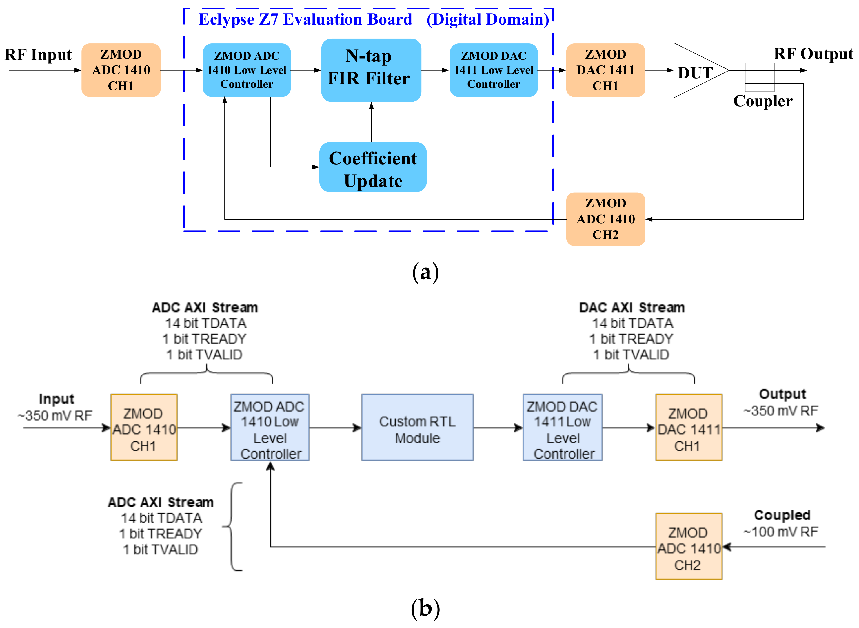
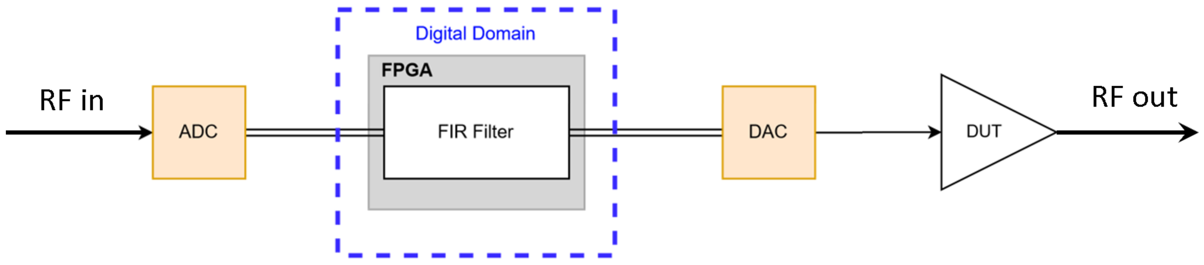
3. Implementation of Digital Predistortion Topology

Figure 3 provides a block diagram of the connections used to implement the pre-distortion equalizer with an adaptive algorithm on an Eclypse Z7 FPGA board. This figure includes two sub-figures: (a) illustrates the connections and topology, while (b) provides more details on the use of the Advanced eXtensible Interface (AXI) protocol and 14-bit data streams with TREADY and TVALID AXI handshakes.
The design prototype utilizes the pre-distortion topology depicted in Figure 1a. To examine the circuit’s performance using a vector network analyzer (VNA), an ADC was added to the input to make the prototype RF in and RF out. The components selected in Figure 3 are described in the following sections, providing more information about how the system is designed and implemented.

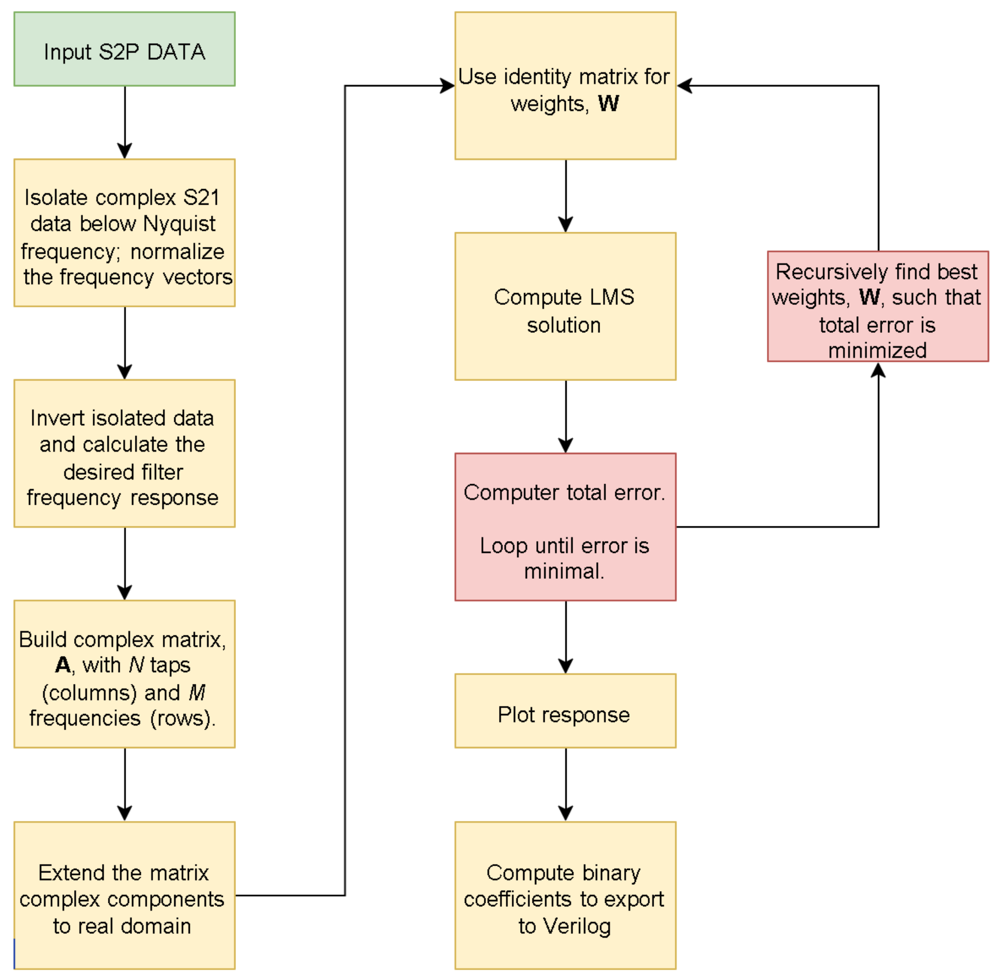
3.1. MATLAB Coefficient Generation

To generate appropriate filter coefficients for our digital equalizer filter, we utilized MATLAB to process the DUT’s s-parameters, configure the least-mean squares algorithm for complex quantities, execute the least-means square algorithm for generating filter coefficients (using matrix operations), easily generate the frequency response created by a filter with those coefficients, calculate the error relative to the ideal response and graphically plot all the results. The design process is illustrated in Figure 4.

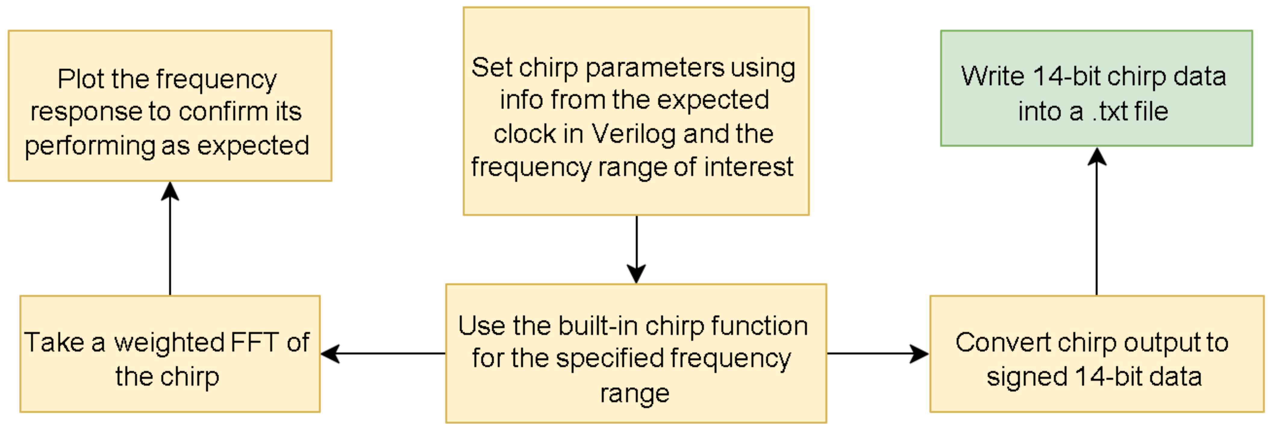
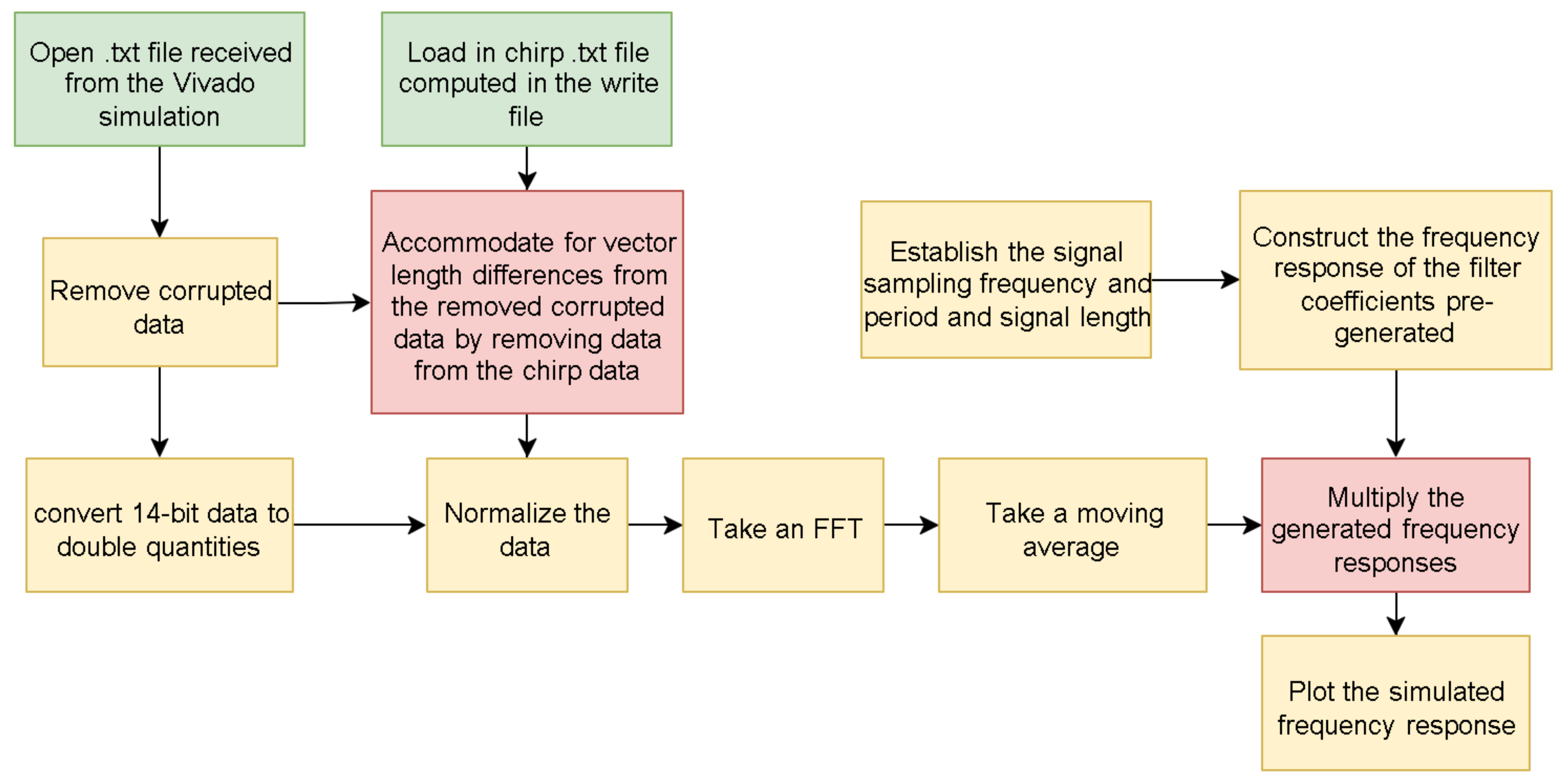
3.2. MATLAB Sweep Read and Write
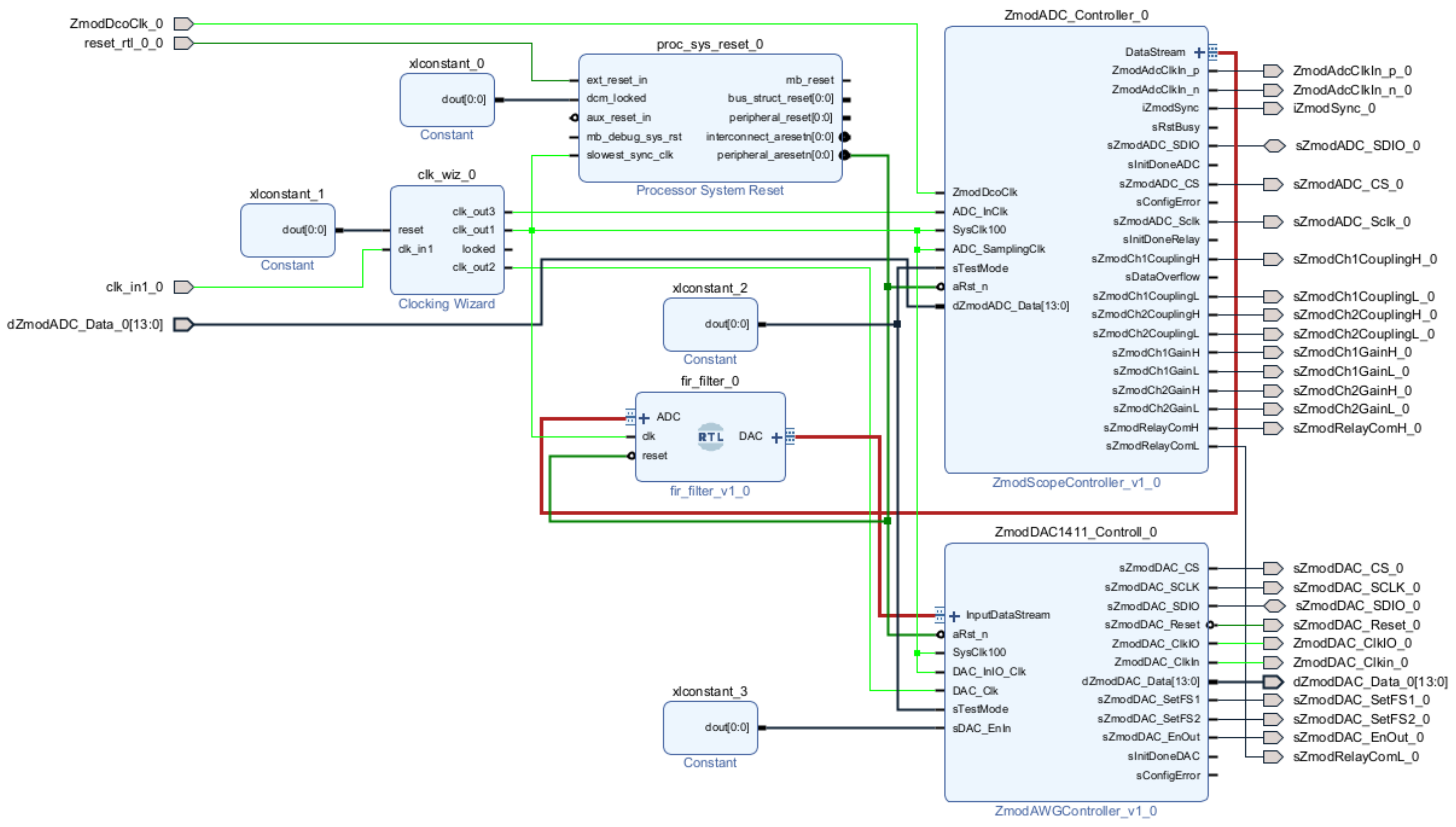
In order to simulate the frequency response on an FPGA board, the chirp signal with a flat magnitude response in a wide range of frequencies is used as the input signal. To simulate the same conditions as the experiment, a sampling time of 10 ns was chosen. The frequency of the chirp signal was set from 100 kHz to 50 MHz, which represents the entire bandwidth for the dynamic equalization case. The signal was converted from a decimal float, which it defaults to in MATLAB, to a signed 14-bit binary number which is used in Verilog. The signal was then saved to a .txt file to be read in Verilog. The Fast Fourier Transform (FFT) of the chirp signal was also done in MATLAB to confirm the flatness of its response. The design of this part is illustrated in the flowchart in Figure 5.
The processed signal from the FPGA is now read into MATLAB for analysis and verification. The output signal was read and cleaned, then converted from a signed 14-bit binary number into a double-precision decimal value. Additionally, the initial signal created in the “write” stage was read for comparison. A sampling time of 10 ns was used in order to calculate the corresponding frequencies of the signals. The output signal was padded with zeroes due to a size mismatch with the input signal, caused by the delayed processing of the signal in the FPGA. The Fourier transform of both signals was taken using the fast Fourier transform and then processed. A moving average of 300 data points was taken in order to minimize the effects of noise near the endpoints. Additionally, the frequency response due to the filter coefficients was imported. Finally, the Verilog simulation output, the simulation input, and the MATLAB simulated filter responses were plotted alongside each other for comparison. This process is illustrated in the flowchart in Figure 6.

3.3. Verilog Design

The project board was set to the Eclypse Z7 board file, which was provided by Digilent’s repository. The constraints file was also obtained from Digilent’s repository, which provided the pin assignments of the FPGA, that could then be subsequently used in the IP Integrator.
In the IP Integrator, a clocking wizard was used to set 4 separate clocks from the 125 MHz Zybo clock: 200 MHz for the ADC System Clock, 100 MHz for the DAC System Clock, 100 MHz for the ADC and DAC Sampling Clock, and 100 MHz for the custom RTL (Register Transfer Level) module. Furthermore, a Processor System Reset IP module was implemented for the resetting of the Zybo Z7 to communicate with the custom RTL module, ADC, and DAC.
All input and output connections (other than the tdata, tready, tvalid streams) were automated by the IP Integrator automated connector as depicted in Figure 7. As well known, the FIR filter works through delays, multiplications and additions. The custom RTL module included a circular buffer register, where in an input was set to the first register and the previous registers were shifted. This results in a delay for each input by some integer N along the circular buffer. Since the FIR filter works at 100 MHz each input is delayed by 10 ns. Every cycle they are delayed again and so forth.
Using this circular buffer, delayed_data, each component is taken and multiplied by the fixed, signed 16-bit valued fir coefficients, fir_coefficient that were pre-calculated in MATLAB. Since the input is signed 14 bit, and the multiplier is signed 16 bit, the output results in signed 30-bit. Each term is summed together with an accumulator and then truncated to signed 14-bit. The DAC_tdata is set to this 14-bit value, which is the “FIR filter time data”. This cycle repeats every 10 ns.
To testbench this module, different valued inputs were required. As such, MATLAB read and write sweep programs were used to generate a sweep signal. The input was taken every 10 ns (100 MHz sampling) similar to the sampling rate of the ADC. The reset and ADC_tready and DAC_tvalid were tested as well to determine if the AXI stream handshake worked properly.
Finally, dynamic equalization was implemented using the aforementioned LMS adaptive algorithm. Feedback was returned to ADC CH2 (from post DUT equalization). The error was determined by subtracting this value from a delayed input stream. For the k t h FIR coefficient, the error was multiplied by the current input delayed by 10 k ns, as shown in Equation (3) [21].

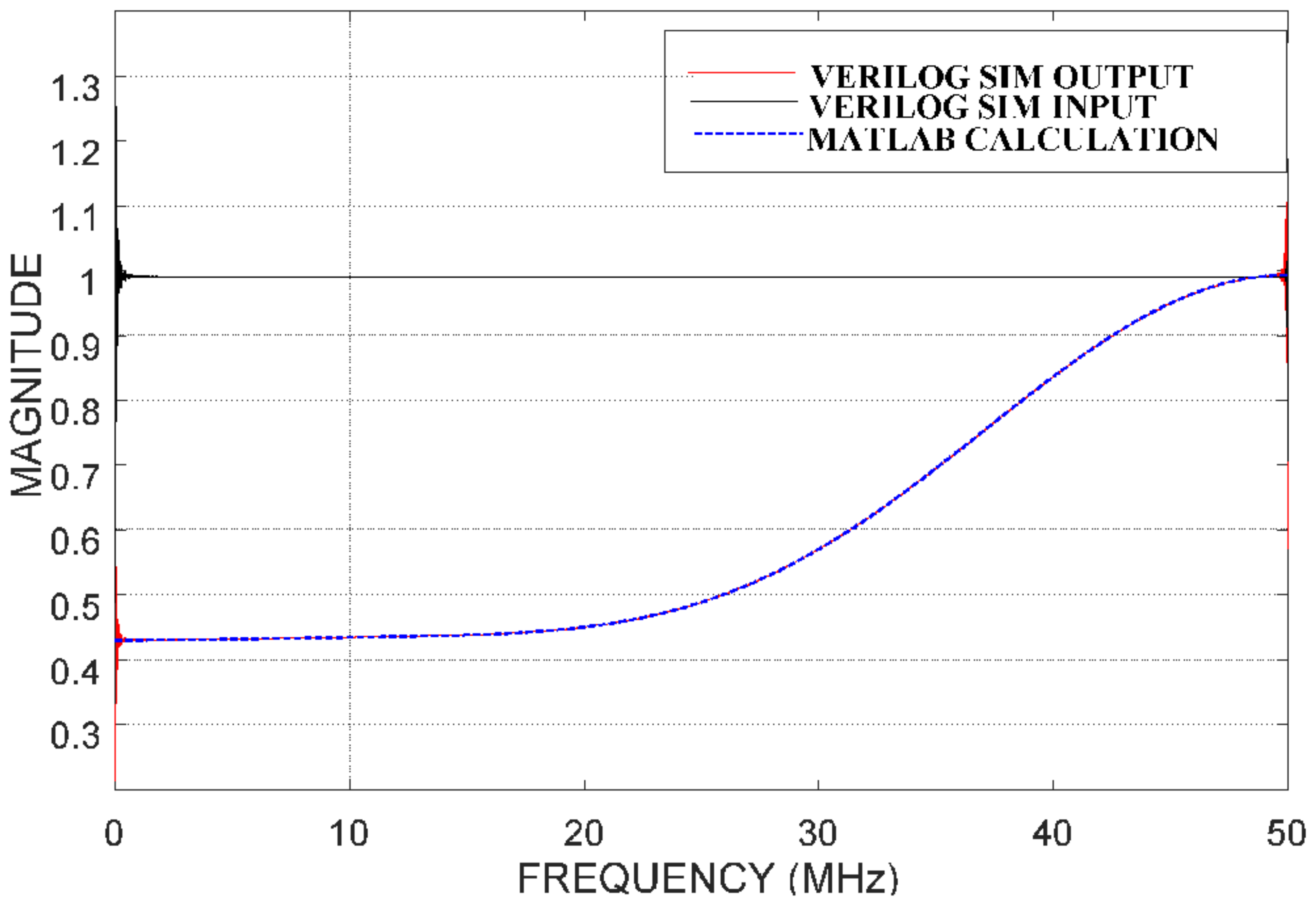
4. Module Testing and Experimental Results

4.1. Software Test

The two core design pieces that needed to be simulated were the filter coefficients through MATLAB and the comparison of the chirp signal FPGA simulations of the passthrough and the filter core artificially programmed into it.
The goal of the coefficient simulation in MATLAB was to alter the filter coefficients until its frequency response multiplied with the frequency response of the DUT that had no more than 2 dB ripple over the specified frequency band and maintained a mostly constant group delay. With the FPGA simulations in Vivado, it was required to generate a time domain signal that could test the filter for comparison with the frequency response shown from the MATLAB simulation. One way to perform this was by generating a chirp signal, this chirp signal can characterize the frequency response of the device since it can be tuned to predictably cover all the specified frequencies over a predictable period of time.
The primary goal of the Vivado simulations was to show that the filter frequency response shown in MATLAB simulations from the set of coefficients designed beforehand was very close to the frequency response shown in Vivado. In doing this it was expected to get somewhat of a better idea of what limitations of the FPGA may do to the filter performance and how the design could potentially be altered to compensate for them with more work.
The output file was used to save the corresponding FIR waveforms so that the Fourier Transform could then be taken in the Sweep Read MATLAB.

4.2. RTL Module Simulation
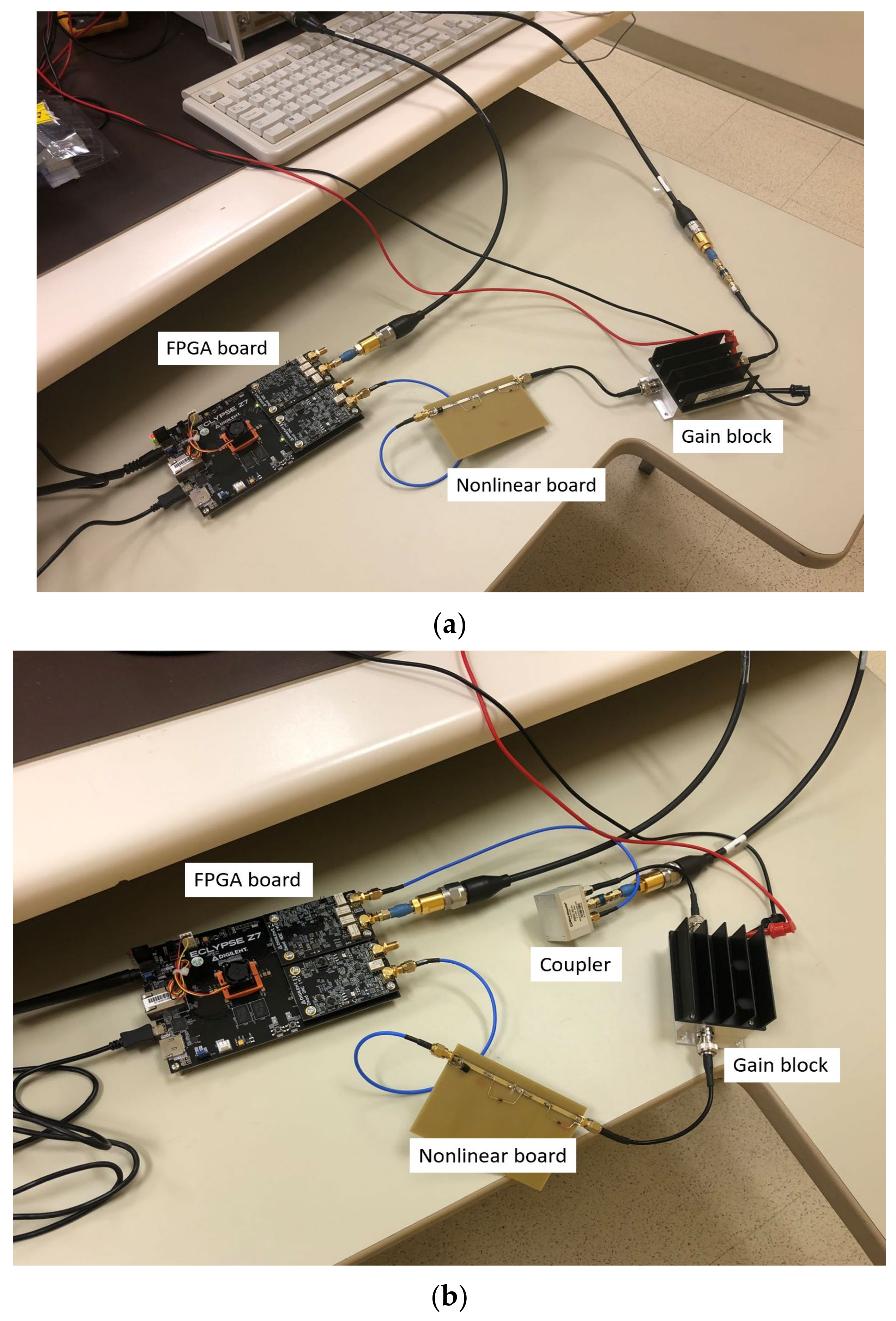
Simulations were done over a 10 ms period to fit the 10 kHz to 50 MHz chirp signal. The filtered analog signal is read out into a text file. After data processing, the frequency response is plotted in Figure 8. There is a negligible error (due to the chirp frequency response) between the expectation (blue dash) and the simulation (red solid).

4.3. Hardware Test

The hardware testing was divided into three main parts: testing the DUT which consists of a self-made nonlinear board and a commercial off-the-shelf gain block, testing the static digitally equalized system prototype, and testing the dynamical digitally equalized system prototype.
The purpose of the static prototype testing was to see whether or not the performance of the filter coefficients (derived beforehand in the algorithm) that were programmed into the FPGA followed the frequency performance that was expected on a VNA. Once the single set of coefficients was performing equalization of the RF system to an acceptable level it was time to test the performance of the dynamic Verilog algorithm programmed on the FPGA.
The filter coefficients found from the development of the static equalizer were used as the initial coefficient guess into the dynamic equalizer. The performance baselines used in all the equalized prototype system tests were to show that the magnitude frequency performance didn’t change (ripple) more than 2 dB and that the group delay flatness remained within 10 ns error of the mean (almost entirely constant) for as much of the chosen frequency band as possible.

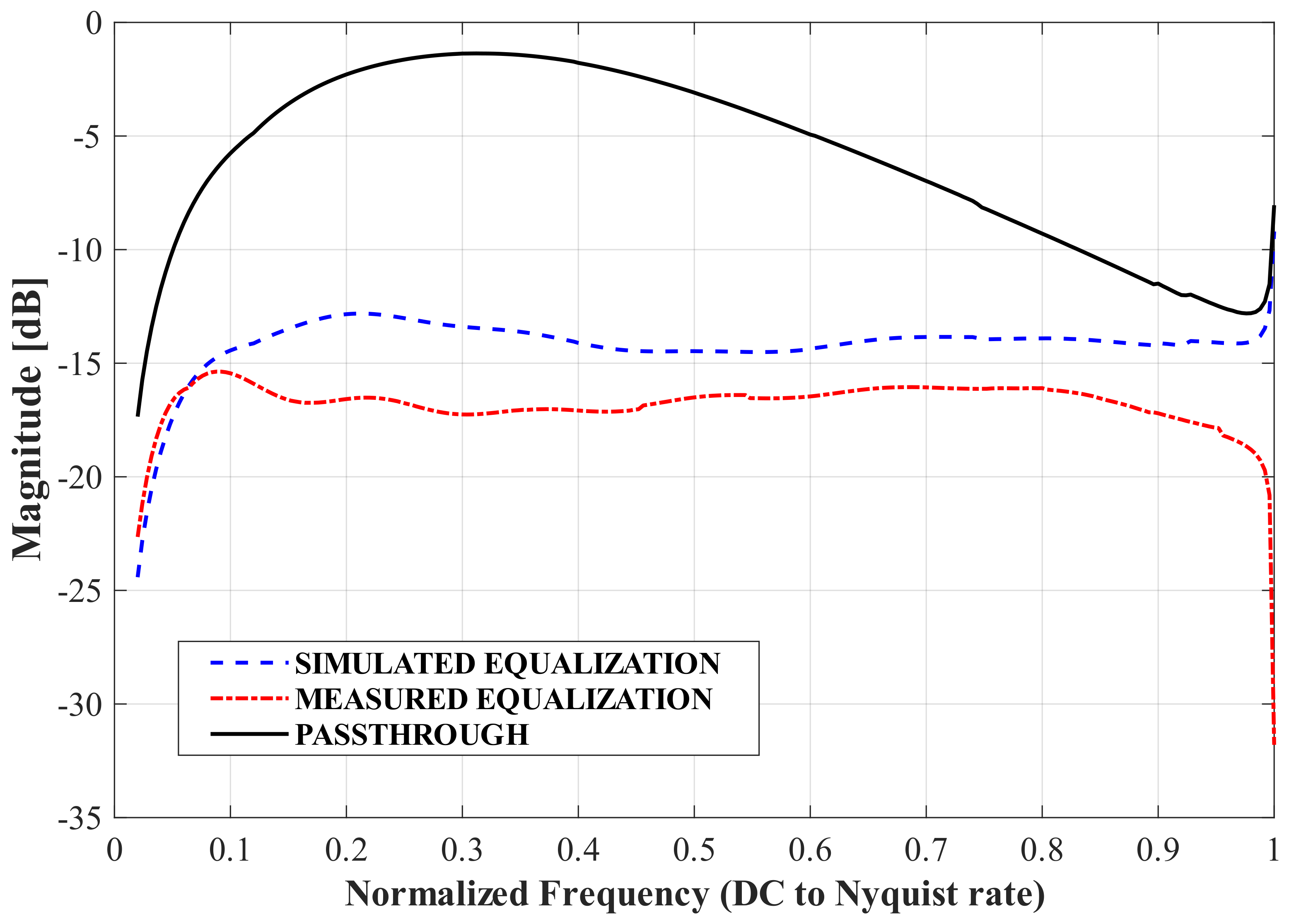
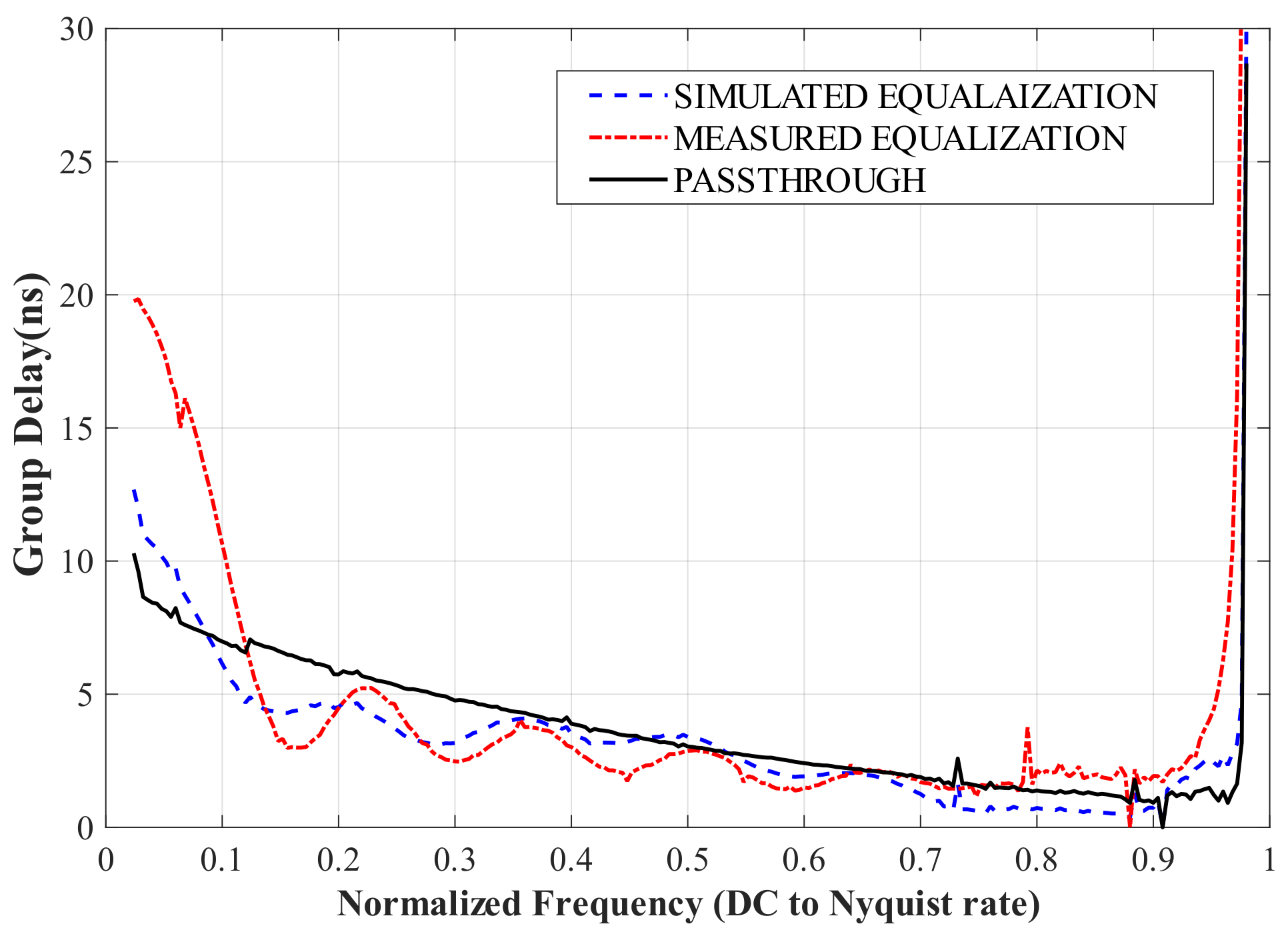
4.4. Static Equalization Results

With the aid of MATLAB, a 15-tap filter was found with coefficients. The frequency response was simulated and then the coefficients were implemented into the RTL. Figure 9 contains two parts that illustrate the hardware connections for both static predistortion equalization and adaptive predistortion equalization. Figure 9a shows the hardware connections for static predistortion equalization, and Figure 9b shows the hardware connections for adaptive predistortion equalization which will be discussed in the next section. In the static predistortion configuration, the ADC module attached on the Eclypse Z7 initially converted the RF signal from VNA port 1. Once processed for static predistortion on the FPGA, the resulting pre-distorted digital signal was then transformed into RF using a DAC module. The digital-to-analog converted signal was next injected into the DUT, which was composed of a self-constructed nonlinear board and a gain block. The final output from the gain block was connected to port 2 of the VNA, thereby completing the setup. Figure 10 shows the static block diagram, while Figure 11 presents the simulations and measurements of the response for the static structure. Furthermore, Figure 12 displays the measured group delay. The simulation and measurement results presented in Figure 11 demonstrate the effectiveness of the proposed equalization technique in improving the amplitude performance of RF front-ends in the static mode. The plots indicate a significant reduction in distortion magnitude, resulting in a cleaner and more accurate signal. Furthermore, Figure 12 shows the measured group delay of the system, revealing less than 10 ns delay variation across the frequency range of 0.1–0.9 Nyquist frequency. These results confirm the validity of our design approach.

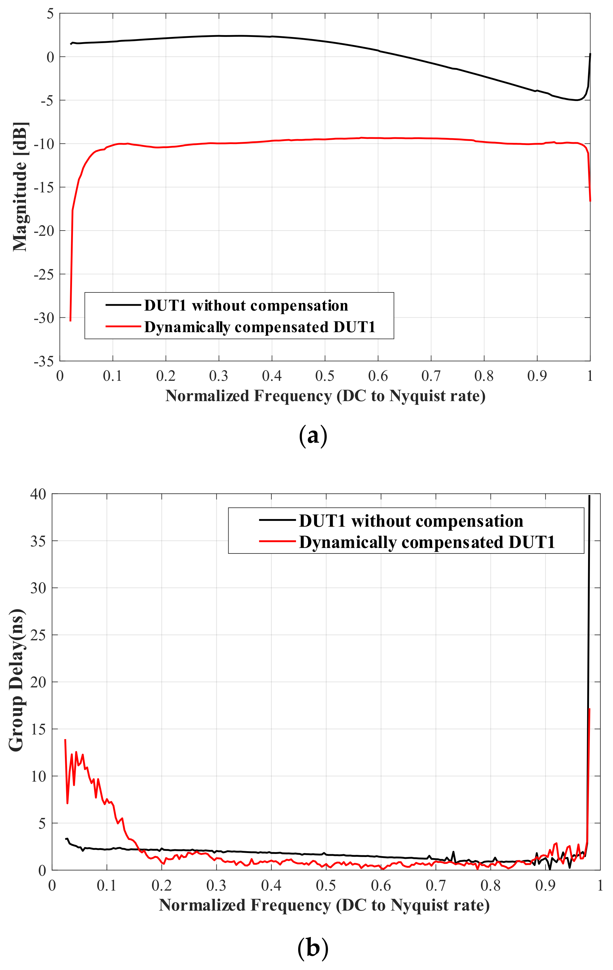
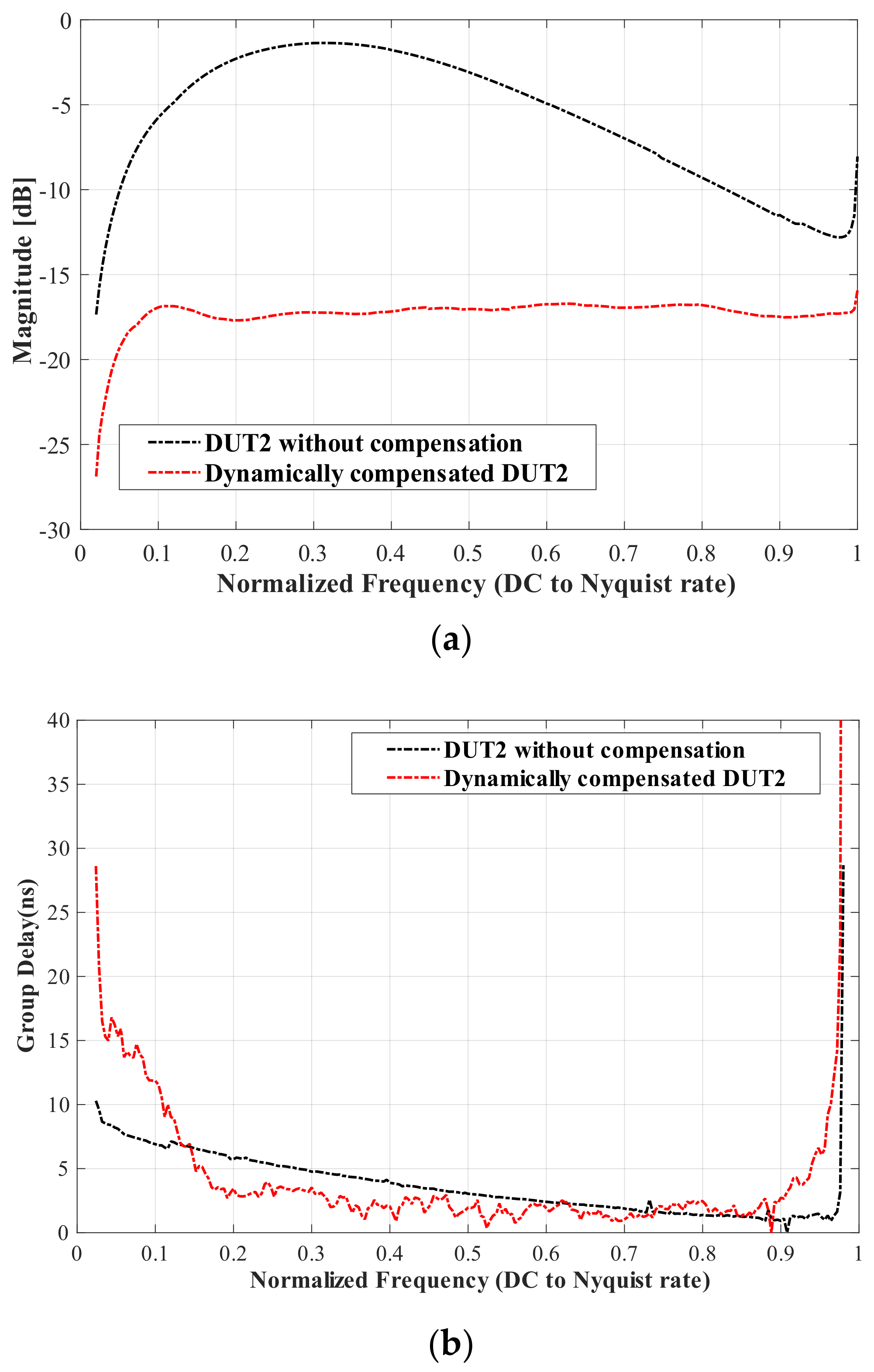
4.5. Dynamic Equalization Results

After obtaining promising results from the static equalization, the filter coefficients were used as the starting point for synthesizing the program. The program wasimplemented, and a bitstream was generated, which was then programmed onto the Eclypse Z7. The system was connected as pictured in Figure 9b, following the block diagram in Figure 3. It can be seen that the RF signal, originating from VNA port 1, was converted by the ADC and subsequently transmitted to the FPGA for predistortion processing. The resulting predistorted digital signal was then converted back into RF form by utilizing the DAC module and was subsequently injected into the DUT, which again consists of a self-constructed nonlinear board and a gain block. The output generated by the gain block was connected to the primary path of a directional coupler, leading to port 2 of the VNA, while the feedback path of the coupler was linked to the FPGA for signal correction purposes.
The frequency response of a unequalized setting (bypassing the FIR configuration in the FPGA) was measured using CH2 of the DAC. Then the frequency response of equalization was measured using CH1 of the DAC for comparison. Differing nonlinear boards cascaded by the same gain block were used as DUT #1 and #2. The magnitude response and group delays of the corresponding situations were plotted in Figure 13 and Figure 14. It can be found that our proposed adaptive digital equalizer exhibited excellent performance in the 0.2–0.8 Nyquist frequency range.

5. Conclusions

In this paper, we proposed an innovative digital equalizer by using an adaptive LMS algorithm and implemented it onto a Digilent Eclypse Z7 FPGA platform that used a Zmod DAC and Zmod ADC. This work presents a new technique for adaptive equalization in RF front-ends, which has not been explored before. In essence, this method derives FIR filter coefficients by measuring the S-parameters of the DUT in real-time, without designing a standard FIR filter. The study’s contribution lies in its unique approach, which can improve the performance of communication systems. The prototype used a predistortion topology with a coupled feedback loop. In this way, adaptive equalization within 2 dB bandwidth was demonstrated in the 0.2–0.8 Nyquist frequency range (10–40 MHz in our case). At this range, the equalizer kept the phase response relatively linear with a group delay flatness less than 10 ns. Different DUT configurations were dynamically examined to validate the design concept. It is worth mentioning that our proposed methodology can be employed in a significantly broader bandwidth scenario. However, we have opted for a narrow bandwidth due to the inherent restrictions of the ADC and DAC speed on the Eclypse Z7 FPGA platform. It is foreseeable that our proposed adaptive digital equalizer has a broad range of applications in wireless communication systems.

Author Contributions

Conceptualization, Z.Z.; methodology, B.N.; software, B.N., Y.L. and Z.Z.; validation, Z.Z. and Y.L.; formal analysis, B.N., Z.Z. and Y.L.; investigation, Z.Z. and Y.L.; resources, Z.Z.; data curation, Z.Z. and Y.L.; writing—original draft preparation, B.N.; writing—review and editing, Z.Z. and Y.L.; visualization, B.N., Z.Z. and Y.L.; supervision, Z.Z. All authors have read and agreed to the published version of the manuscript.

Funding

This research received no external funding.

Data Availability Statement

The dataset is not applicable.

Conflicts of Interest

The authors declare no conflict of interest.

References

  1. Choi, K.S.; Kim, J.H.; Ahn, D.; Jeong, N.H.; Pack, J.K. Trends in rain attenuation model in satellite system. In Proceedings of the 13th International Conference on Advanced Communication Technology (ICACT2011), Gangwon-Do, Republic of Korea, 13–16 February 2011; pp. 1530–1533. [Google Scholar]
  2. Dudley, D.G. Wireless propagation in circular tunnels. IEEE Trans. Antennas Propag. 2005, 53, 435–441. [Google Scholar] [CrossRef]
  3. Pingenot, J.; Rieben, R.; White, D. Full wave analysis of RF signal attenuation in a lossy cave using a high order time domain vector finite element method. In Proceedings of the IEEE/ACES International Conference on Wireless Communications and Applied Computational Electromagnetics, Honolulu, HI, USA, 3–7 April 2005; pp. 658–661. [Google Scholar] [CrossRef]
  4. Siles, G.A.; Riera, J.M.; Garcia-del-Pino, P. Atmospheric Attenuation in Wireless Communication Systems at Millimeter and THz Frequencies [Wireless Corner]. IEEE Antennas Propag. Mag. 2015, 57, 48–61. [Google Scholar] [CrossRef]
  5. Dulk, G.A.; Erickson, W.C.; Manning, R.; Bougeret, J.L. Calibration of low-frequency radio telescopes using the galactic background radiation. Astron. Astrophys. 2001, 365, 294–300. [Google Scholar] [CrossRef]
  6. Winder, S. Analog and Digital Filter Design; Newnes: Amsterdam, The Netherlands, 2007. [Google Scholar]
  7. Der Ziel, A. Thermal noise in field-effect transistors. In Proceedings of the IRE; IEEE: New York, NY, USA, 1962; Volume 50, pp. 1808–1812. [Google Scholar]
  8. Lin, Y.-S.; Chen, C.-Z.; Yang, H.-Y.; Chen, C.-C.; Lee, J.-H.; Huang, G.-W.; Lu, S.-S. Analysis and Design of a CMOS UWB LNA With Dual-RLC-Branch Wideband Input Matching Network. IEEE Trans. Microw. Theory Tech. 2010, 58, 287–296. [Google Scholar] [CrossRef]
  9. Wu, C.; Lin, Y.; Lee, J.; Wang, C. A 2.87 ± 0.19 dB NF 3.1∼10.6 GHz ultra-wideband low-noise amplifier using 0.18 µm CMOS technology. In Proceedings of the 2012 IEEE Radio and Wireless Symposium, Santa Clara, CA, USA, 15–18 January 2012; pp. 227–230. [Google Scholar] [CrossRef]
  10. Lathi, B.P. Principles of Signal Processing and Linear Systems; Oxford University Press: Oxford, UK, 2009. [Google Scholar]
  11. Borth, D.E.; Gerson, I.A.; Haug, J.R.; Thompson, C.D. A flexible adaptive FIR filter VLSI IC. IEEE J. Sel. Areas Commun. 1988, 6, 494–503. [Google Scholar] [CrossRef]
  12. Lucky, R.W. Techniques for adaptive equalization of digital communication systems. Bell Syst. Tech. J. 1966, 45, 255–286. [Google Scholar] [CrossRef]
  13. Moulines, E.; Duhamel, P.; Cardoso, J.; Mayrargue, S. Subspace methods for blind identification of multichannel FIR filters. IEEE Trans. Signal Process. 1995, 43, 516–525. [Google Scholar] [CrossRef]
  14. Widrow, B.; Stearns, S.D. Adaptive Signal Processing; Prentice-Hall: Engelwood Cliffs, NJ, USA, 1985. [Google Scholar]
  15. Haykin, S. Adaptive Filter Theory, 3rd ed.; Prentice-Hall: Engelwood Cliffs, NJ, USA, 1996. [Google Scholar]
  16. Lo, B.C.W.; Letaief, K. Adaptive equalization and interference cancellation for wireless communication systems. IEEE Trans. Commun. 1999, 47, 538–545. [Google Scholar] [CrossRef]
  17. Kollar, I.; Rolain, Y. Complex correction of data acquisition channels using FIR equalizer filters. IEEE Trans. Instrum. Meas. 1993, 42, 920–924. [Google Scholar] [CrossRef]
  18. Johnson, R.; Schniter, P.; Endres, T.J.; Behm, J.D.; Brown, D.R.; Casas, R.A. Blind equalization using the constant modulus criterion: A review. Proc. IEEE 1998, 86, 1927–1950. [Google Scholar] [CrossRef]
  19. John, P.G.; Dimitris, M.G. Digital Signal Processing Principles, Algorithms, and Applications, 3rd ed.; Prentice-Hall: Engelwood Cliffs, NJ, USA, 1996. [Google Scholar]
  20. Smith, J.O., III. Spectral Audio Signal Processing; W3K Publishing: Berlin, German, 2011. [Google Scholar]
  21. Lai, Y.T.; Kao, C.C.; Chen, H.J. Design and Implementation of an Adaptive FIR Filter Based on Delayed Error LMS Algorithm. In Proceedings of the 1999 IEEE Workshop on Signal Processing Systems. SiPS 99. Design and Implementation (Cat. No.99TH8461), Taipei, Taiwan, 22 October 1999; pp. 704–712. [Google Scholar] [CrossRef]
Figure 1. Application scenarios of the proposed adaptive FIR equalizer (a) in the transmitting path and (b) in the receiving path.
Electronics 12 02010 g001
Figure 2. The general topology of an adaptive FIR filter.
Electronics 12 02010 g002
Figure 3. Block diagram of the connections on an Eclypse Z7 FPGA board to implement the predistortion equalizer with an adaptive algorithm; (a) illustrates the connections and topology; (b) shows where the AXI protocol takes place and the use of 14-bit data streams with TREADY and TVALID AXI handshakes.
Electronics 12 02010 g003
Figure 4. Flowchart for generating filter coefficients using weighted LMS algorithm.
Electronics 12 02010 g004
Figure 5. Flowchart illustrating the process of generating a chirp signal in MATLAB, converting it to a Verilog-compatible format, and saving it to a .txt file for use in the Verilog testbench.
Electronics 12 02010 g005
Figure 6. Flowchart for comparing Verilog simulation output, MATLAB simulated filter response, and imported filter coefficients using the chirp signal read from a .txt file.
Electronics 12 02010 g006
Figure 7. IP block diagram of the IP Cores and custom RTL module in Vivado.
Electronics 12 02010 g007
Figure 8. Frequency response comparison of expected (blue dash) and simulated (red solid).
Electronics 12 02010 g008
Figure 9. Hardware connection of (a) Static predistortion equalization and (b) Adaptive predistortion equalization.
Electronics 12 02010 g009
Figure 10. Block diagram of the connections to implement the static predistortion equalizer, corresponding to Figure 9a.
Electronics 12 02010 g010
Figure 11. The magnitude response of the system in the static mode: without equalization (black solid), simulated equalization (blue dash), and measured equalization (red dash-dot).
Electronics 12 02010 g011
Figure 12. The group delay of the system in the static mode: without equalization (black solid), simulated equalization (blue dash), and measured equalization (red dash-dot).
Electronics 12 02010 g012
Figure 13. The magnitude response (a) and group delay (b) of the system with DUT #1 in the dynamic mode.
Electronics 12 02010 g013
Figure 14. The magnitude response (a) and group delay (b) of the system with DUT #2 in the dynamic mode.
Electronics 12 02010 g014
Disclaimer/Publisher’s Note: The statements, opinions and data contained in all publications are solely those of the individual author(s) and contributor(s) and not of MDPI and/or the editor(s). MDPI and/or the editor(s) disclaim responsibility for any injury to people or property resulting from any ideas, methods, instructions or products referred to in the content.

