Article

Design of a GaAs-Based Ka-Band Low Noise Amplifier MMIC with Gain Flatness Enhancement

1
Communication Center, Institute of Microelectronics of the Chinese Academy of Sciences, Beijing 100029, China
2
University of Chinese Academy of Sciences, Beijing 101408, China
3
Beijing Key Laboratory of New Generation Communication RF Technology, Beijing 100029, China
*
Author to whom correspondence should be addressed.
Electronics 2023, 12(10), 2325; https://doi.org/10.3390/electronics12102325
Submission received: 19 April 2023 / Revised: 9 May 2023 / Accepted: 18 May 2023 / Published: 21 May 2023
(This article belongs to the Special Issue Advanced Design of RF/Microwave Circuit)

Abstract

:
This paper presents a GaAs-based Ka-band low noise amplifier (LNA) with gain flatness enhancement. Active device optimization and inductive degeneration techniques were employed to obtain a low noise figure (NF) and good input/output return loss. In order to achieve a flat gain response over a wide bandwidth, the stagger tuning technique was utilized. The proposed LNA was implemented by 0.15 μ m GaAs pHEMT process, and the chip area is only 1.5 × 0.9 mm 2 . Measurement results show that the presented LNA exhibits a small signal gain of 21.5 ± 0.3 dB, and the NF of the LNA is less than 2.2 dB from 32 to 40 GHz at room temperature.

1. Introduction

The number of wireless devices, along with the amount of data, has increased dramatically over the last two decades, necessitating wireless systems with greater communication capacity and higher data rates. However, radio spectrum resources for wireless communication are scarce, and radio frequency (RF) bands have been densely allocated for various commercial and military applications. There is a growing interest in millimeter-wave wireless systems. “Ka-band” refers to electromagnetic waves in the frequency range of 26.5–40 GHz. The millimeter wave frequency bands used for 5G communication are mostly in Ka-band, such as 28, 37, and 39 GHz in the United States, 26 GHz in Europe, and 26 GHz and 40 GHz in China [1]. In addition, satellite communication systems [2] and passive millimeter wave imaging [3,4,5] also operate in Ka-band.
The low noise amplifier is the first active module of the receiver, and its performance is directly related to the receiver’s dynamic range and sensitivity. Low noise amplifiers are expected to have extremely low noise figures, high gain, good input and output return loss, low power consumption, and good linearity [6]. However, gain flatness is often an overlooked indicator. Good gain flatness can ensure that the signal has an approximate amplification degree in the band and relax the requirements for the dynamic range of the analog–digital converter (ADC) [7], so it has notable research significance.
Several circuit topologies for broadband low-noise amplifiers have been reported, such as distributed amplifiers, shunt feedback amplifiers, and filter-matching network amplifiers. Distributed amplifiers [8,9] can achieve wide bandwidth with low input and output return loss but at the expense of power consumption and area. The feedback amplifier [10,11] can expand the amplifier’s bandwidth, but it tends to degrade the noise performance; the filter-matching network amplifier [12] can achieve broadband frequency response, but excessive passive components increase the loss of input matching, deteriorating the noise figure. Ref. [13] demonstrated a wide bandwidth, low noise amplifier with source degeneration and resistive feedback that achieved a gain greater than 25 dB but with poor gain flatness. A 32–50 GHz low noise amplifier has a gain of 28 dB but a noise figure of 2.8 dB [14]. The LNA in Reference [15] exhibits a gain flatness of 1.2 dB and NF of 2.2–2.6 dB, but its gain is limited. Reference [16] presented a low noise amplifier using resistive and inductive feedback techniques that achieved a gain of 19.8 dB and a gain flatness of 0.8 dB, but it did not show the measurement data of the noise figure. The gain flatness of the low-noise amplifier can be further improved while maintaining high gain, a low noise figure, low power consumption, and a small chip area.
In this paper, we propose a compact gain flatness enhancement wide-band low noise amplifier. To achieve simultaneous input and noise matching, the inductive degeneration technique is employed, and the stagger tuning technique is used to improve gain flatness. The designed LNA was implemented through a 0.15 μ m GaAs pHEMT process. The measurement results show that the proposed LNA achieves a gain of 21.5 dB with a gain flatness of ±0.3 dB. The measured noise figure at room temperature is below 2.2 dB from 32 to 40 GHz. The LNA draws 17 mA from a 3.3 V power supply. The designed LNA realizes the organic combination of low noise figure, high gain, good gain flatness, low power consumption, and small chip area.
The paper is organized as follows: Section 2 introduces the design methodology of the circuit in detail, including active device optimization, inductive degradation technology, and stagger tuning technique. The experimental results and performance comparison table with the state-of-the-art mm-wave wideband LNAs are presented in Section 3. Finally, the paper is concluded in Section 4.

2. Circuit Design

A three-stage common-source cascade topology is utilized in this design, as can be seen in Figure 1. Inductive degeneration [17] is utilized in the first stage in order to achieve simultaneous input and noise matching [18]. The stagger tuning technique is employed to achieve flat gain. The first stage uses a 4 × 25 μ m CPW transistor for low noise figure, and the second and third stages use a 2 × 50 μ m MS transistor for high gain.
For ease of use, the proposed LNA is powered by a single power supply. A resistor divider network and a large resistor or a quarter-wavelength transmission line comprise the biasing network. R6 is a large resistor with a resistance value of 10 k Ω which serves as a DC choke in a wide frequency range. Bypass capacitors are added to the gate bias and drain bias of each stage in order to filter out interference signals from power supplies, substrates, etc. R4, R7, and R11 are small resistors with a resistance value of 5 Ω , reducing signals’ cross talk between amplifier stages and improving circuit stability.
In the input matching design, although the high-order LC network can be used to achieve broadband matching, excessive components will increase the insertion loss of the matching network and further deteriorate the noise. Therefore, in this design, simple T-type matching is adopted, in which C1 serves as a DC blocker.

2.1. Active Device Optimization

To a large extent, the performance of the transistor determines the upper limit of the LNA’s performance; thus, it is critical to select the appropriate transistor type, bias point, and size. For low-noise amplifiers, the most critical indicators are noise figure and gain. Correspondingly, the minimum noise figure (NF m i n ) and the maximum available gain (max available gain, MAG) can be used to evaluate the performance of transistors.
The adopted 0.15 μ m GaAs pHEMT process provides two types of transistors. One has no back holes on the source terminal and is called a coplanar waveguide (CPW) transistor; the other has back holes on both sides of the source terminal and is called a microstrip (MS) transistor. The two types of transistors are simulated and compared in detail.
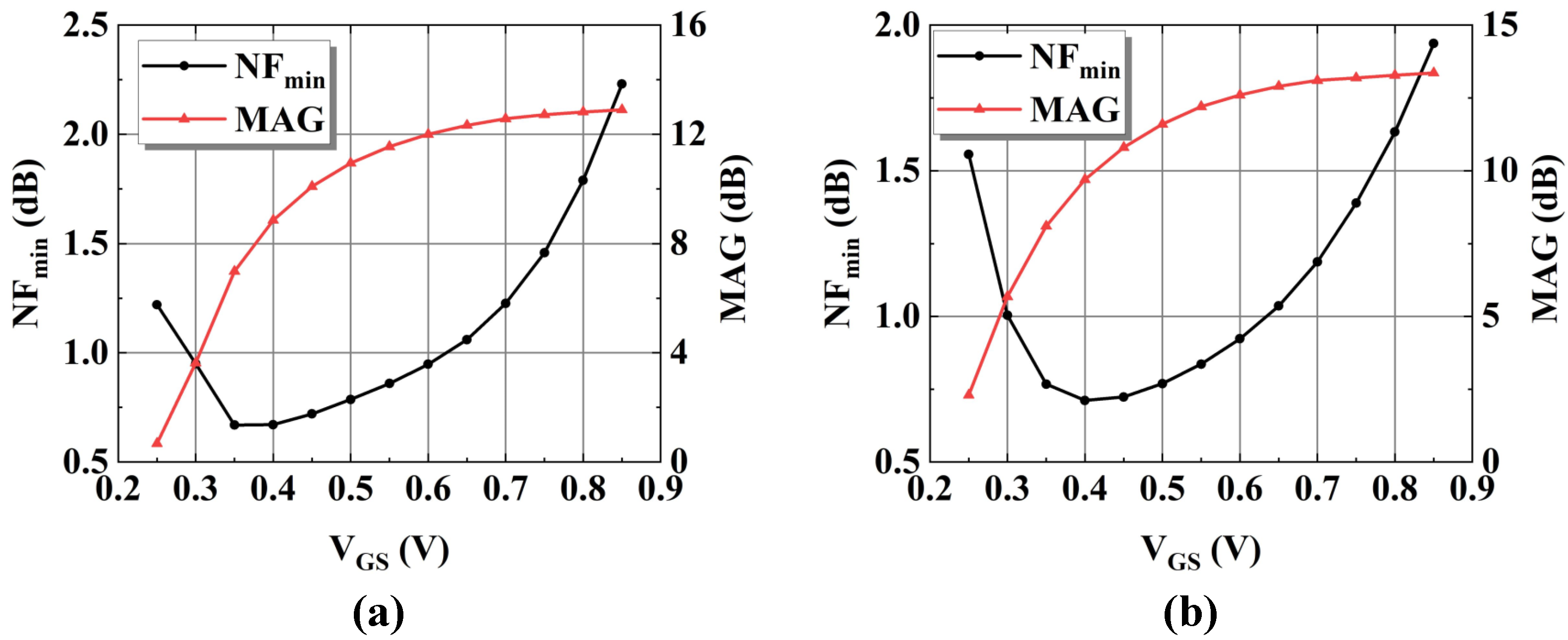
First, NF m i n and MAG under different values of V G S are simulated in order to determine the optimal bias point. In the simulation, V D D is fixed at 3.3 V, which is the power supply voltage of this design; the frequency is determined to be 36 GHz. V G S is swept from 0.25 V to 0.85 V, and the step size is set to 0.05 V. Figure 2 depicts the simulation results.
The simulation results show that as V G S increases, NF m i n decreases and then increases, and there exists an optimal bias voltage V G S 0 , which minimizes the NF m i n . In contrast, MAG increases rapidly with V G S increase, and then the magnitude of the increase slows down, indicating a monotonous increasing trend overall. It can be seen from Figure 2a that for the CPW transistor, NF m i n reaches a minimum value when V G S is around 0.4 V, but its MAG is relatively low. After carefully considering the noise figure and gain characteristics, V G S is set to 0.45 V. Similarly, the MS transistor exhibits the same law, with V G S set to 0.45 V as the bias point.
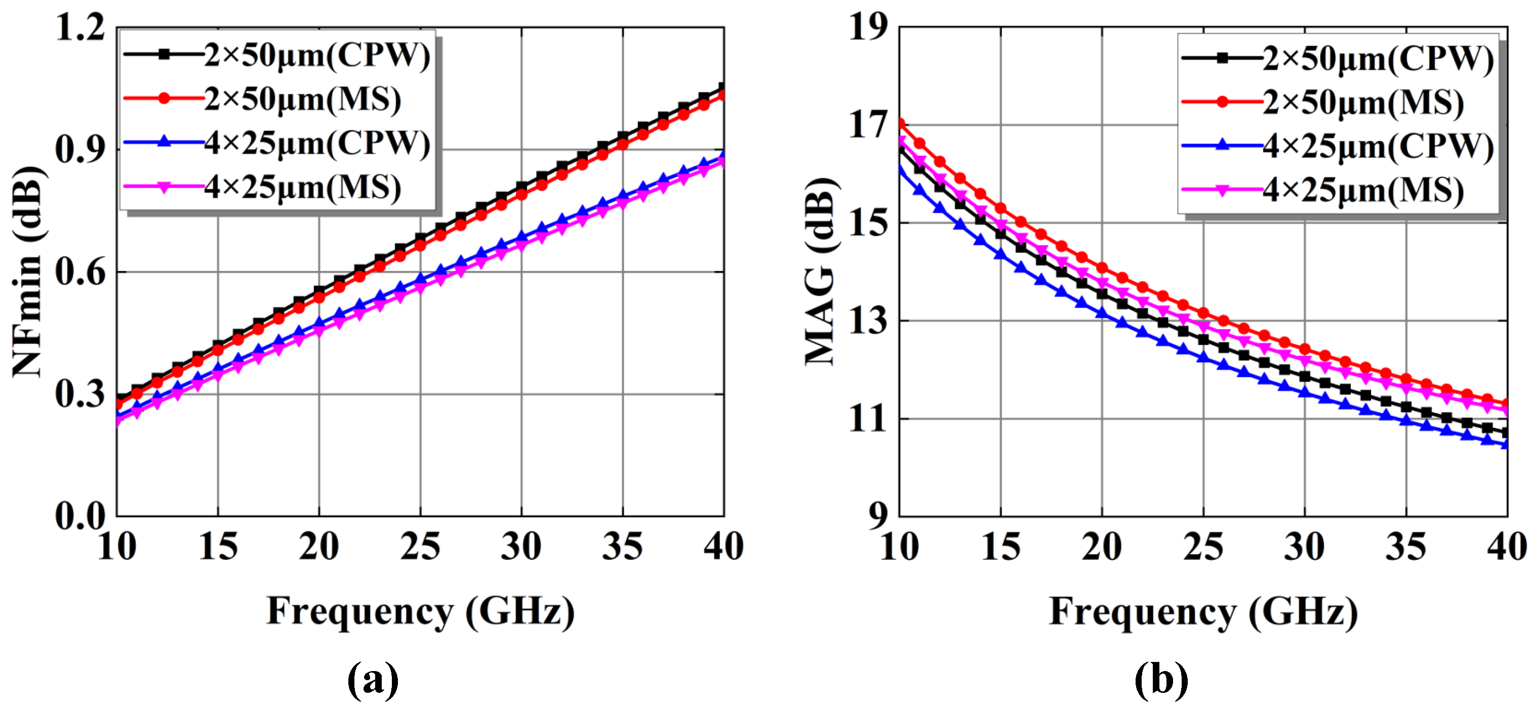
After determining the optimal bias point, the NF m i n and MAG of various-size transistors were simulated. Figure 3 depicts the simulated result.
Figure 3 indicates that: (1) For the same transistor type, the NF m i n of 4 × 25 μ m is lower than that of 2 × 50 μ m, owing to the smaller gate parasitic resistance of the multi-finger transistor, thereby reducing the noise caused by resistance. In addition, the MAG of 4 × 25 μ m is also lower than that of 2 × 50 μ m. (2) For transistors of the same size, the NF m i n of the CPW transistor and the MS transistor are almost equal, but the MAG of the MS transistor is higher than that of the CPW transistor.
The transistor type, bias point, and size are determined based on the above simulation results. Since the first stage employs the inductive degeneration technique, a 4 × 25 μ m CPW transistor is used in the first stage to achieve a lower noise figure. The second and the third stages use a 2 × 50 μ m MS transistor to meet the gain requirement.

2.2. Inductive Degeneration

The inductive degeneration technique is widely used in the design of low-noise amplifiers [19]. By connecting an inductor in series with the source terminal of the transistor, the input impedance is derived as
Z i n ( s ) = 1 s C g s + s ( L G + L S ) + g m L S C g s
where L G and L S are the series gate and degenerated inductances, respectively. C g s is the gate-to-source capacitance [20]. As shown in Equation (1), the real part of the input impedance is g m L S /C g s , and it is frequency independent. The L S reduces the distance between the optimal noise impedance point and the maximum gain impedance point.
The optimal noise impedance point Z o p t and the maximal gain impedance point Z m a g are defined as follows:
Z o p t ( s ) = R o p t + j X o p t
Z m a g ( s ) = R m a g + j X m a g
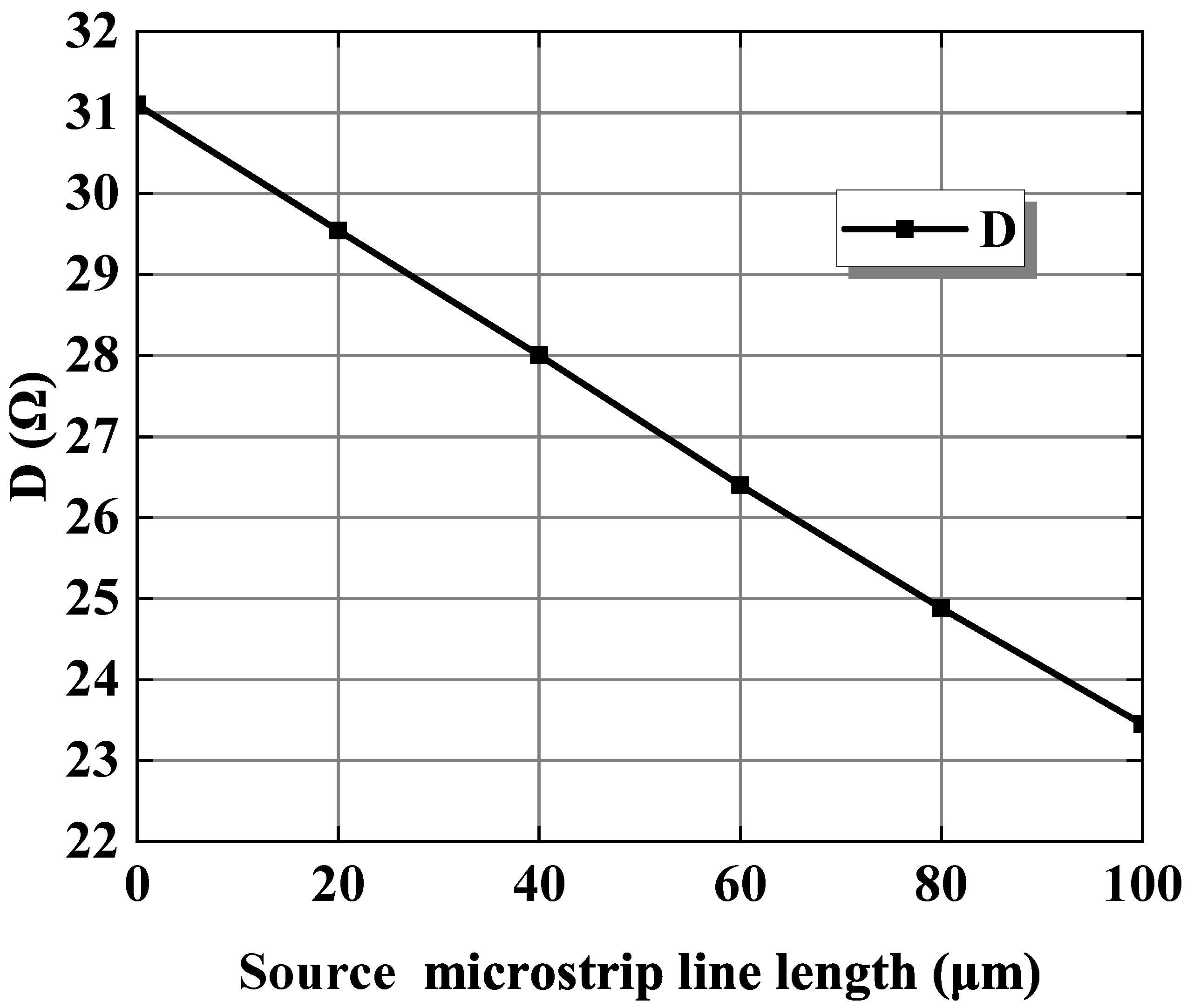
A new parameter D is defined here to characterize the distance between two impedance points, Z o p t and Z m a g , and the definition formula for D is shown in Equation (4).
D = R m a g R o p t 2 + X m a g X o p t 2
The L S in Figure 1 is implemented by a short microstrip line. The variation curve of D is simulated for various source microstrip line lengths’. As shown in Figure 4, D decreases monotonically as the length of source microstrip line increases, implying that the inductive degeneration technique makes it easier to achieve both noise and input matching.
Adding L S will not worsen the noise, but it can bring the distance between the two impedance points closer, allowing for simultaneous input and noise matching. However, L S cannot be increased arbitrarily, as the increase of Ł S lowers the gain. As a result, the value of L S should take into account two factors. Figure 5 depicts the simulated NF m i n and MAG at various source microstrip line lengths. NF m i n decreased slightly as L S increased, but MAG decreased rapidly. Considering that the first stage should still maintain a specific gain, the source microstrip line length is determined to be 60 μ m.

2.3. Gain Flatness Enhancement

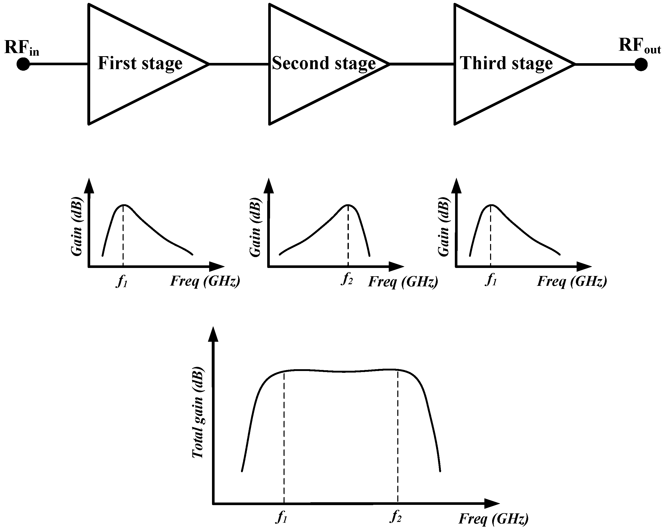
For broadband and flat gain, the stagger tuning technique was adopted. The basic idea of stagger tuning is to distribute the center frequencies of different amplifier stages at various frequency points so that a flat frequency response can be obtained [21]. In this design, the gain peak frequencies of each stage are set at two different frequency points f 1 and f 2 , as shown in Figure 6. Compared with the amplifier that distributes the gain peak at multiple frequency points, the amplifier that distributes the peak gain at two frequency points can maximize the gain, bandwidth, and noise figures within the target band [22]. The peak gain frequency of the first and third stages is designed to be around 29 GHz, and the peak gain frequency of the second stage is 39 GHz. Therefore, the proposed LNA obtains a flat gain response from 32 to 40 GHz.

2.3.1. Gain Analysis of the First Stage

The output matching network of the first stage, which includes C 2 , C 3 , L 3 , and L 4 , primarily determines the resonant frequency of the amplifier’s first stage. C i n 2 represents all the second-stage transistor gate capacitances, including C g s 2 , Miller equivalent capacitance, and other parasitic capacitances. C d s 1 is the parasitic capacitance of M 1 , assuming that the drain-to-source resistance is infinite. The small-signal equivalent model of the first stage is shown in Figure 7, where Z 1 represents the impedance seen from node A to the second stage. Z 1 can be calculated as follows:
Z 1 ( s ) = s L 3 + 1 s C 2 + s L 4 ( 1 s C 3 + 1 s C i n 2 ) = s 4 L 4 C 3 C i n 2 C 2 L 3 + s 2 [ C 2 ( C i n 2 + C 3 ) ( L 3 + L 4 ) + L 4 C i n 2 C 3 ] + C i n 2 + C 3 s 3 L 4 C 3 C i n 2 C 2 + s C 2 ( C i n 2 + C 3 )
The gain of the source-degenerated common-source amplifier A v 1 (s) is
A v 1 ( s ) g m 1 1 + g m 1 s L S ( Z 1 ( s ) 1 s C d s 1 )
where g m 1 is the transconductance of the first stage’s transistor and L S is the source degenerated inductance. Equation (5) shows that Z 1 (s) has three poles p 11 , p 12 , and p 13 , respectively.
p 11 = 0
p 12 , 13 = ± j C i n 2 + C 3 L 4 C 3 C i n 2
As the transistor size and bias point are determined, C i n 2 and C d s 1 are also determined. The frequency of the first-stage amplifier’s gain peak can be modified by adjusting the L 3 , L 4 , C 2 , and C 3 , especially for L 4 and C 3 . After careful design and optimization, it is finally determined that L 4 is 0.16 nH and C 3 is 0.24 pF.

2.3.2. Gain Analysis of the Second Stage

Similarly, the gain of the second stage is determined by the output matching network of the second stage. Figure 8 depicts the small-signal equivalent model of the second stage of the proposed LNA. R 8 and C 5 form a parallel RC network to improve the stability of the circuit. Since the parallel network is between the second and third stage, it does not degrade the noise figure. C i n 3 represents the sum of C g s 3 of the transistor of the third stage, the Miller equivalent capacitance, and other parasitic capacitances. Z 2 denotes the impedance seen from node B to the third stage, and Z 2 can be calculated as:
Z 2 ( s ) = 1 s C 4 + s L 5 + 1 s C i n 3 + R 8 1 s C 5 = s 3 C 5 R 8 C i n 3 L 5 C 4 + s 2 C i n 3 L 5 C 4 + s R 8 ( C 5 C i n 3 + C 4 C 5 + C 4 C i n 3 ) + C 4 + C i n 3 s 2 C 5 R 8 C i n 3 C 4 + s C 4 C i n 3
The gain of the second-stage amplifier A v 2 (s) is:
A v 2 ( s ) = g m 2 ( Z 2 ( s ) 1 s C d s 2 )
where g m 2 is the transconductance of the second-stage transistor. C d s 2 is the parasitic capacitance of M 2 , neglect the drain-to-source resistance. Z 2 (s) has two poles p 21 and p 22 , respectively.
p 21 = 0
p 22 = 1 C 5 R 8
The frequency distribution of the gain peak of the second-stage amplifier can be adjusted by changing the values of L 5 , C 4 , and C 5 . Simulations were performed to obtain the appropriate value of components. When L 5 is 80 pH, C 4 is 0.67 pF, and C 5 is 0.35 pF, the frequency response of the second stage, as shown in Figure 9, is realized.

2.3.3. Gain Analysis of the Third Stage

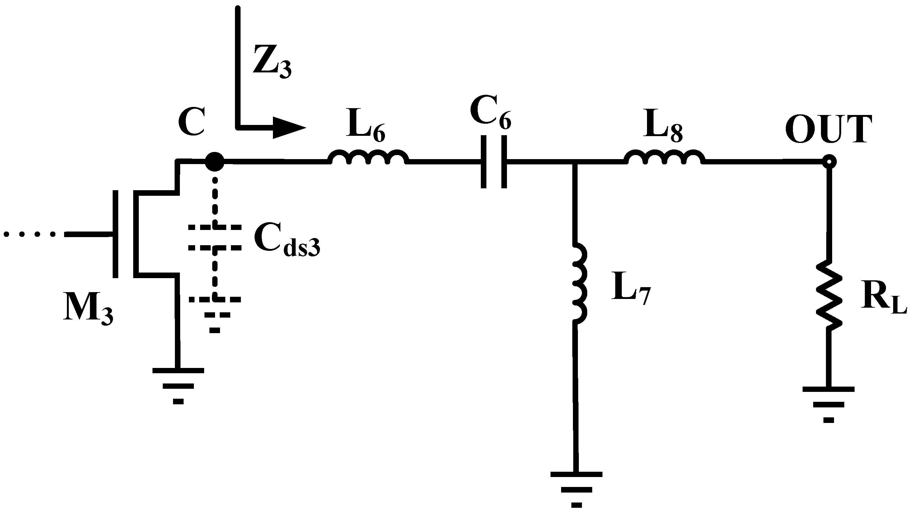
Figure 10 shows a small-signal equivalent model of the third stage of the proposed LNA. R L is the load impedance, and its value is 50 Ω . The impedance seen from node C to the output terminal Z 3 can be calculated as:
Z 3 ( s ) = s L 6 + 1 s C 6 + s L 7 s L 8 + R L = s 3 C 6 ( L 6 L 7 + L 6 L 8 + L 7 L 8 ) + s 2 C 6 R L ( L 6 + L 7 ) + s ( L 7 + L 8 ) + R L s 2 C 6 ( L 7 + L 8 ) + s C 6 R L
Gain of the third-stage amplifier A v 3 (s) is:
A v 3 ( s ) = g m 3 ( Z 3 ( s ) 1 s C d s 3 )
In Equation (14), g m 3 is the transconductance of the third-stage transistor. C d s 3 is the parasitic capacitance of M 3 ; the drain-to-source resistance is also neglected. Z 3 (s) has two pole p 31 and p 32 :
p 31 = 0
p 32 = R L L 7 + L 8
The frequency distribution of the gain peak of the third-stage amplifier can be adjusted by changing the values of L 6 , L 7 , L 8 , and C 6 . The peak gain of the third stage is distributed at 29 GHz, achieving a wide-band and flat gain together with the first two stages. Through simulation, it is determined that L 6 , L 7 , and L 8 are 0.18 nH, 0.4 nH, and 0.04 nH, respectively. The parasitic inductance of the back hole is also considered, and C 6 is 0.25 pF.
Based on the above analysis, the value of each component is determined. Figure 9 shows each stage’s simulated power gain. Through careful design, the peak gains of the first and third stages are distributed at 29 GHz, and the peak gain of the second stage is distributed at 39 GHz. The proposed LNA achieves a very flat gain in the target frequency band owing to the dual-frequency stagger tuning technique.

3. Experimental Results

The Ka-band LNA was implemented in a 0.15 μ m GaAs pHEMT technology with a substrate thickness of 100 μ m. Figure 11 shows the micrograph of the chip, and it has a total area of 1.5 × 0.9 mm 2 , including all the test pads. The LNA draws 17 mA from the supply at a V D D of 3.3 V.
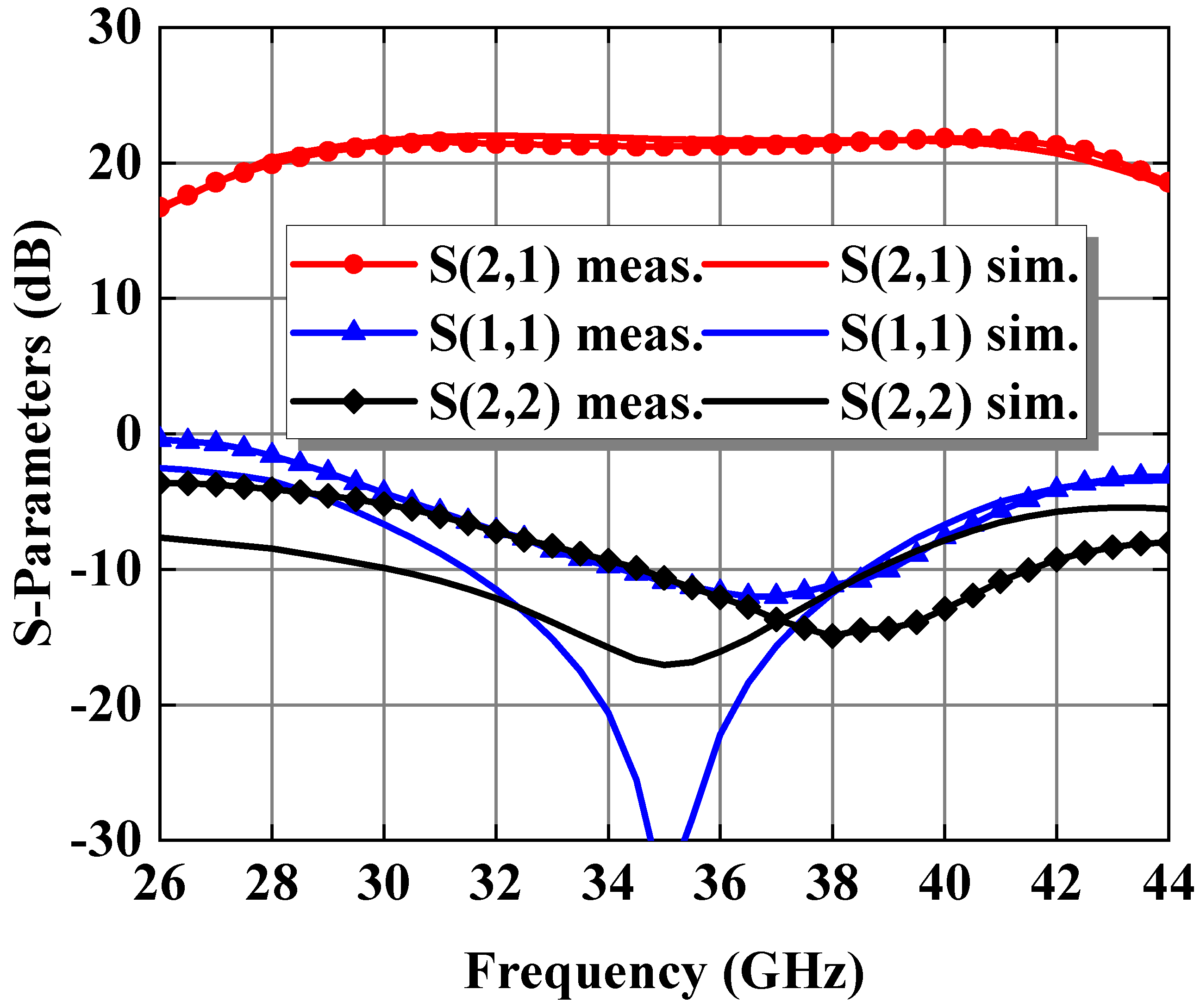
Figure 12 shows the measured and simulated S-parameters of the proposed Ka-band LNA with flat gain. It exhibits a typical small signal gain of 21.5 dB, and its gain flatness reaches ±0.3 dB in the frequency range of 32 to 40 GHz. There are slight differences between the simulated and measured results of S11 and S22, mainly manifested as frequency shift. Among them, S11 shifts about 2 GHz towards the high-frequency end, and S22 shifts about 3 GHz towards the high-frequency end, which is mainly caused by process fluctuations and parasitic factors. In addition, the reduction of the Q value also deteriorates S11, mainly because the simulator underestimates the parasitic resistance of components (transmission line, capacitor).
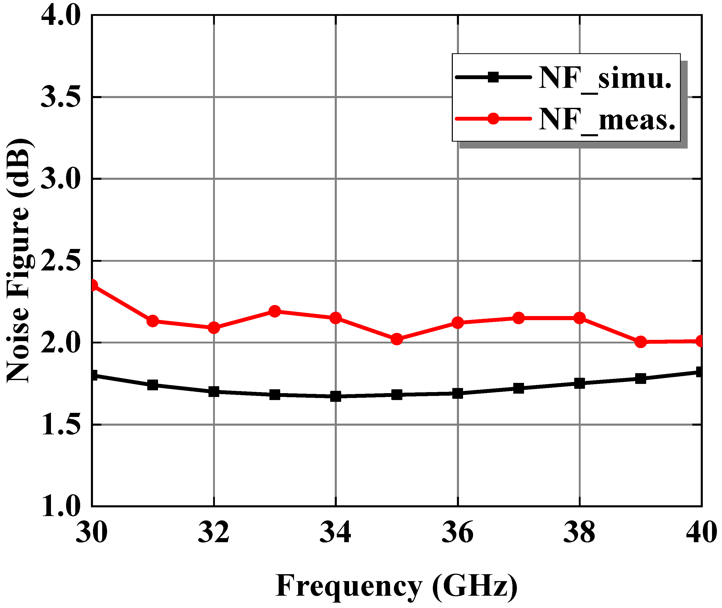
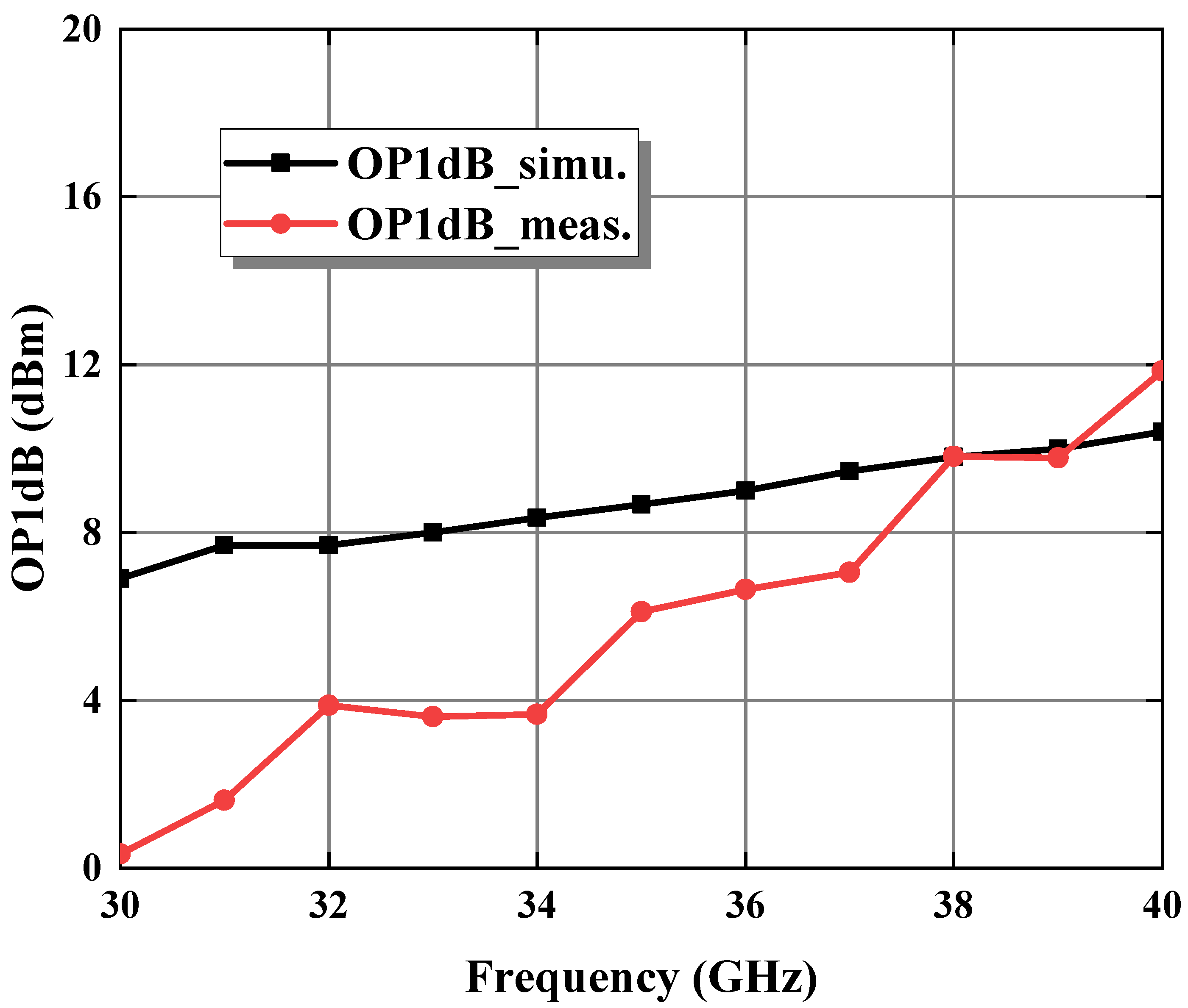
The measured and simulated noise figure are given in Figure 13. The LNA achieves NF of 2–2.2 dB from 32 to 40 GHz. The output 1dB compression point (OP1dB) was measured in order to verify the linearity of the LNA, as shown in Figure 14. The LNA achieves an OP1dB of 4–12 dBm from 32 to 40 GHz, achieving high linearity with limited power consumption. The performance of the proposed wideband LNA is summarized and compared with the state-of-the-art mm-wave wideband LNAs in Table 1.

4. Conclusions

A compact, low-power-consumption Ka-band LNA with gain flatness enhancement in a 0.15 μ m GaAs pHEMT technology has been presented. The inductive degeneration technique was employed in order to achieve simultaneous input and noise matching. To enhance the gain flatness, the LNA adopts the stagger tuning technique. By distributing the peak gains at two different frequency points, a wide band and flat gain was obtained. The proposed LNA exhibits ±0.3 dB gain variation while maintaining a high gain of 21.5 dB. The noise figure is lower than 2.2 dB from 32 to 40 GHz. Moreover, it occupies only 1.5 × 0.9 mm 2 and consumes a DC power of 56 mW.

Author Contributions

Conceptualization, Z.Y., K.W., Y.F., X.L. and Y.Y.; methodology, Z.Y., K.W., X.L. and Y.Y.; software, Z.Y. and Y.F.; validation, Z.Y., K.W. and Y.F.; data curation, Z.Y. and Y.F.; writing—original draft preparation, Z.Y. and K.W.; writing—review and editing, Z.Y., X.L. and Y.Y. All authors have read and agreed to the published version of the manuscript.

Funding

This research received no external funding.

Data Availability Statement

Not applicable.

Conflicts of Interest

The authors declare no conflict of interest.

References

  1. Hu, S.; Wang, F.; Wang, H. A 28-/37-/39-GHz Linear Doherty Power Amplifier in Silicon for 5G Applications. IEEE J. Solid-State Circuits 2019, 54, 1586–1599. [Google Scholar] [CrossRef]
  2. Schwantuschke, D.; Aja, B.; Seelmann-Eggebert, M.; Quay, R.; Leuther, A.; Bruckner, P.; Schlechtweg, M.; Mikulla, M.; Kallfass, I.; Ambacher, O. Q- and E-Band Amplifier MMICs for Satellite Communication. In Proceedings of the 2014 IEEE MTT-S International Microwave Symposium (IMS2014), Tampa, FL, USA, 1–6 June 2014; IEEE: Piscataway, NJ, USA, 2014; pp. 1–4. [Google Scholar]
  3. Yujiri, L.; Shoucri, M.; Moffa, P. Passive Millimeter Wave Imaging. IEEE Microw. Mag. 2003, 4, 39–50. [Google Scholar] [CrossRef]
  4. Yujiri, L. Passive Millimeter Wave Imaging. In Proceedings of the 2006 IEEE MTT-S International Microwave Symposium Digest, San Francisco, CA, USA, 11–16 June 2006; pp. 98–101. [Google Scholar]
  5. Gong, J.; Chen, X.; Hu, A.; Miao, J. Design of a V-Band Low Noise Amplifier for Passive Millimeter Wave Imaging Application. Microelectron. J. 2022, 126, 105491. [Google Scholar] [CrossRef]
  6. Wan, Q.; Wang, C. Design of 3.1–10.6 GHz Ultra-Wideband CMOS Low Noise Amplifier with Current Reuse Technique. AEU-Int. J. Electron. Commun. 2011, 65, 1006–1011. [Google Scholar] [CrossRef]
  7. Yu, Y.-H.; Yang, Y.-S.; Chen, Y.-J.E. A Compact Wideband CMOS Low Noise Amplifier with Gain Flatness Enhancement. IEEE J. Solid-State Circuits 2010, 45, 502–509. [Google Scholar] [CrossRef]
  8. Liu, R.C.; Lin, C.S.; Deng, K.L.; Wang, H. A 0.5-14-GHz 10.6-dB CMOS Cascode Distributed Amplifier. In Proceedings of the 2003 Symposium on VLSI Circuits. Digest of Technical Papers (IEEE Cat. No.03CH37408), Kyoto, Japan, 12–14 June 2003; pp. 139–140. [Google Scholar]
  9. Lu, Y.; Yeo, K.S.; Cabuk, A.; Ma, J.; Do, M.A.; Lu, Z. A Novel CMOS Low-Noise Amplifier Design for 3.1- to 10.6-GHz Ultra-Wide-Band Wireless Receivers. IEEE Trans. Circuits Syst. I 2006, 53, 1683–1692. [Google Scholar] [CrossRef]
  10. Kim, C.W.; Kang, M.S.; Anh, P.T.; Kim, H.T.; Lee, S.G. An Ultra-Wideband CMOS Low Noise Amplifier for 3-5-GHz UWB System. IEEE J. -Solid-State Circuits 2005, 40, 544–547. [Google Scholar] [CrossRef]
  11. Zhan, J.H.C.; Taylor, S.S. A 5 GHz Resistive-Feedback CMOS LNA for Low-Cost Multi-Standard Applications. In Proceedings of the 2006 IEEE International Solid State Circuits Conference—Digest of Technical Papers, San Francisco, CA, USA, 6–9 February 2006; pp. 721–730. [Google Scholar]
  12. Ismail, A.; Abidi, A.A. A 3-10-GHz Low-Noise Amplifier with Wideband LC-Ladder Matching Network. IEEE J. -Solid-State Circuits 2004, 39, 2269–2277. [Google Scholar] [CrossRef]
  13. Nguyen, D.P.; Pham, B.L.; Pham, T.; Pham, A.-V. A 14–31 GHz 1.25 DB NF Enhancement Mode GaAs PHEMT Low Noise Amplifier. In Proceedings of the 2017 IEEE MTT-S International Microwave Symposium (IMS), Honololu, HI, USA, 4–9 June 2017; pp. 1961–1964. [Google Scholar]
  14. Weng, S.-H.; Lin, C.-H.; Chang, H.-Y.; Chiong, C.-C. Q-Band Low Noise Amplifiers Using a 0.15 μm MHEMT Process for Broadband Communication and Radio Astronomy Applications. In Proceedings of the 2008 IEEE MTT-S International Microwave Symposium Digest, Atlanta, GA, USA, 15–20 June 2008; pp. 455–458. [Google Scholar]
  15. Yang, L.; Yang, L.-A.; Rong, T.; Li, Y.; Jin, Z.; Hao, Y. Codesign of Ka-Band Integrated GaAs PIN Diodes Limiter and Low Noise Amplifier. IEEE Access 2019, 7, 88275–88281. [Google Scholar] [CrossRef]
  16. Feng, J.-H.; Ye, Y.-F.; Wu, L.-S.; Mao, J.-F. A Ka-Band Broadband Low Noise Amplifier with Resistive and Inductive Feedback. In Proceedings of the 2022 IEEE 4th International Conference on Circuits and Systems (ICCS), Chengdu, China, 23–26 September 2022; pp. 160–163. [Google Scholar]
  17. Lehmann, R.E.; Heston, D.D. X-Band Monolithic Series Feedback LNA. IEEE Trans. Microw. Theory Tech. 1985, 33, 1560–1566. [Google Scholar] [CrossRef]
  18. Nguyen, T.-K.; Kim, C.-H.; Ihm, G.-J.; Yang, M.-S.; Lee, S.-G. CMOS Low-Noise Amplifier Design Optimization Techniques. IEEE Trans. Microw. Theory Tech. 2004, 52, 1433–1442. [Google Scholar] [CrossRef]
  19. Hu, Y.; Chi, T. A 27–46-GHz Low-Noise Amplifier with Dual-Resonant Input Matching and a Transformer-Based Broadband Output Network. IEEE Microw. Wirel. Compon. Lett. 2021, 31, 725–728. [Google Scholar] [CrossRef]
  20. Razavi, B. RF Microelectronics, 2nd ed.; Prentice Hall: Upper Saddle River, NJ, USA, 2012. [Google Scholar]
  21. Liu, J.; Tu, J.; Wu, Y.; Feng, G. Bandwidth Extension Techniques for CMOS Low-Noise Amplifiers. In Proceedings of the 2021 IEEE MTT-S International Wireless Symposium (IWS), Nanjing, China, 23 May 2021; pp. 1–3. [Google Scholar]
  22. Jang, T.H.; Jung, K.P.; Kang, J.-S.; Byeon, C.W.; Park, C.S. 120-GHz 8-Stage Broadband Amplifier with Quantitative Stagger Tuning Technique. IEEE Trans. Circuits Syst. I Regul. Pap. 2020, 67, 785–796. [Google Scholar] [CrossRef]
  23. Yu, Y.-H.; Hsu, W.-H.; Chen, Y.-J.E. A Ka-Band Low Noise Amplifier Using Forward Combining Technique. IEEE Microw. Wirel. Compon. Lett. 2010, 20, 672–674. [Google Scholar] [CrossRef]
  24. Wang, G.; Chen, W.; Liu, J.; Mo, J.; Chen, H.; Wang, Z.; Yu, F. Design of a Broadband Ka-Band MMIC LNA Using Deep Negative Feedback Loop. IEICE Electron. Express 2018, 15, 20180317. [Google Scholar] [CrossRef]
  25. Chen, Y.-M.; Wang, Y.; Chiong, C.-C.; Wang, H. A 21.5-50 GHz Low Noise Amplifier in 0.15-μm GaAs PHEMT Process for Radio Astronomical Receiver System. In Proceedings of the 2021 IEEE Asia-Pacific Microwave Conference (APMC), Brisbane, Australia, 28 November 2021; IEEE: Piscataway, NJ, USA, 2021; pp. 7–9. [Google Scholar]
  26. Chou, Y.-T.; Chiong, C.-C.; Wang, H. A Q-Band LNA with 55.7% Bandwidth for Radio Astronomy Applications in 0.15-μm GaAs PHEMT Process. In Proceedings of the 2016 IEEE International Symposium on Radio-Frequency Integration Technology (RFIT), Taipei, Taiwan, 24–26 August 2016; pp. 1–3. [Google Scholar]
  27. Nikandish, G.; Yousefi, A.; Kalantari, M. A Broadband Multistage LNA with Bandwidth and Linearity Enhancement. IEEE Microw. Wirel. Compon. Lett. 2016, 26, 834–836. [Google Scholar] [CrossRef]
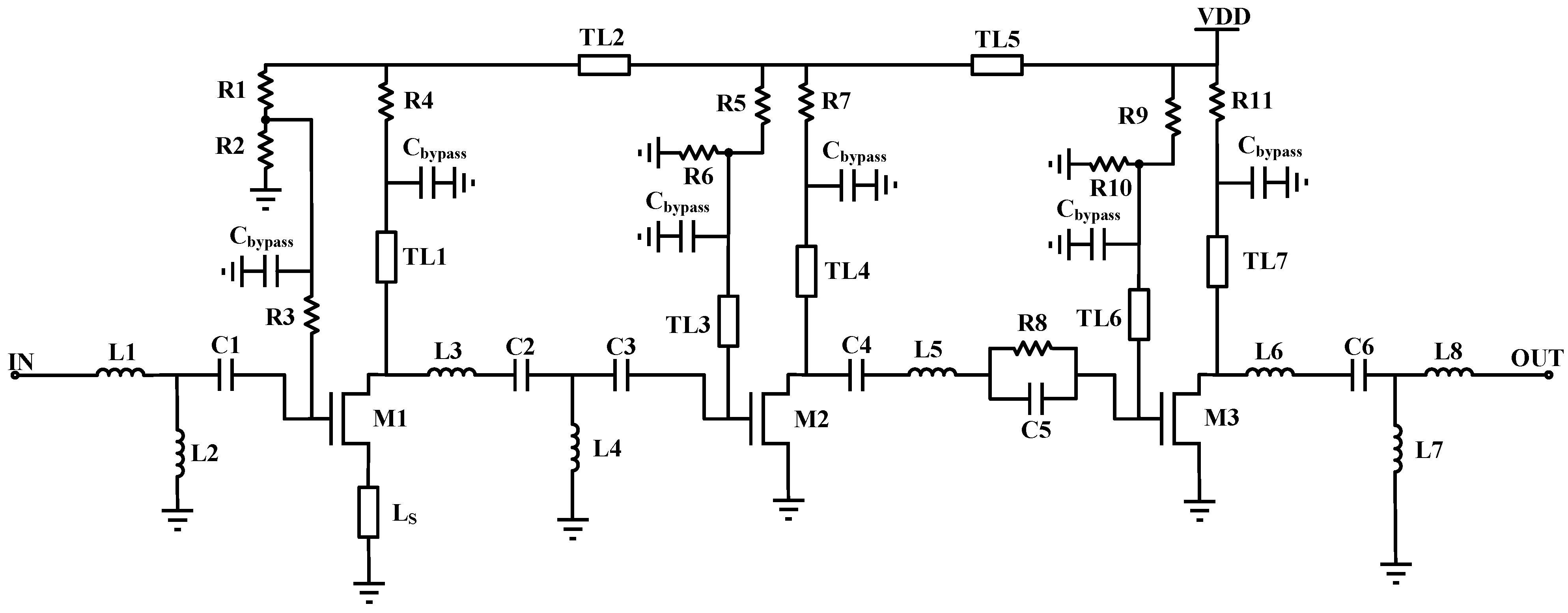
Figure 1. Schematic view of the proposed LNA.
Electronics 12 02325 g001
Figure 2. Simulated NF m i n and MAG of a 4 × 25 μ m (a) CPW; (b) MS transistor versus different values of V G S .
Electronics 12 02325 g002
Figure 3. The simulated (a) NF m i n ; (b) MAG for transistor of different sizes (2 × 50 μ m CPW, 2× 50 μ m MS, 4 × 25 μ m CPW, 4 × 25 μ m MS).
Electronics 12 02325 g003
Figure 4. Simulated D versus different values of the source microstrip line length.
Electronics 12 02325 g004
Figure 5. Simulated NF m i n and MAG versus various values of source microstrip line length.
Electronics 12 02325 g005
Figure 6. Block diagram of the stagger tuning technique.
Electronics 12 02325 g006
Figure 7. Small-signal equivalent model of the first stage.
Electronics 12 02325 g007
Figure 8. Small-signal equivalent model of the second stage.
Electronics 12 02325 g008
Figure 9. Simulated gain of each stage.
Electronics 12 02325 g009
Figure 10. Small-signal equivalent model of the third stage.
Electronics 12 02325 g010
Figure 11. Micrograph of the chip.
Electronics 12 02325 g011
Figure 12. Simulated and measured S-parameters of the design.
Electronics 12 02325 g012
Figure 13. Simulated and measured noise figure.
Electronics 12 02325 g013
Figure 14. Simulated and measured output 1 dB compression point.
Electronics 12 02325 g014
Table 1. Performance of broadband multistage LNAs.
ReferenceThis Work[23][24][25][26][27]
Process0.15-µm GaAs pHEMT0.15-µm InGaAs pHEMT0.15-µm GaAs pHEMT0.15-µm GaAs pHEMT0.15-µm GaAs pHEMT0.1-µm GaAs pHEMT
Frequency (GHz)32–4029–4325–4022.5–3428.5–50.518–43
Gain (dB)21.514.22022.52321.6
Gain flatness (dB)±0.3NA±1.5±1.2±1.5±1.5
NF (dB)2.22–3.32.83–4.53.81.8–2.7
Area (mm 2 )1.5 × 0.90.65 × 0.722.5 × 1.22.5 × 12 × 1.52 × 1
Power (mW)56382303662.6140
Disclaimer/Publisher’s Note: The statements, opinions and data contained in all publications are solely those of the individual author(s) and contributor(s) and not of MDPI and/or the editor(s). MDPI and/or the editor(s) disclaim responsibility for any injury to people or property resulting from any ideas, methods, instructions or products referred to in the content.