

Influence of Bulk Doping and Halos on the TID Response of I/O and Core 150 nm nMOSFETs

 ,
, 

Abstract
1. Introduction
2. Devices and Experiments
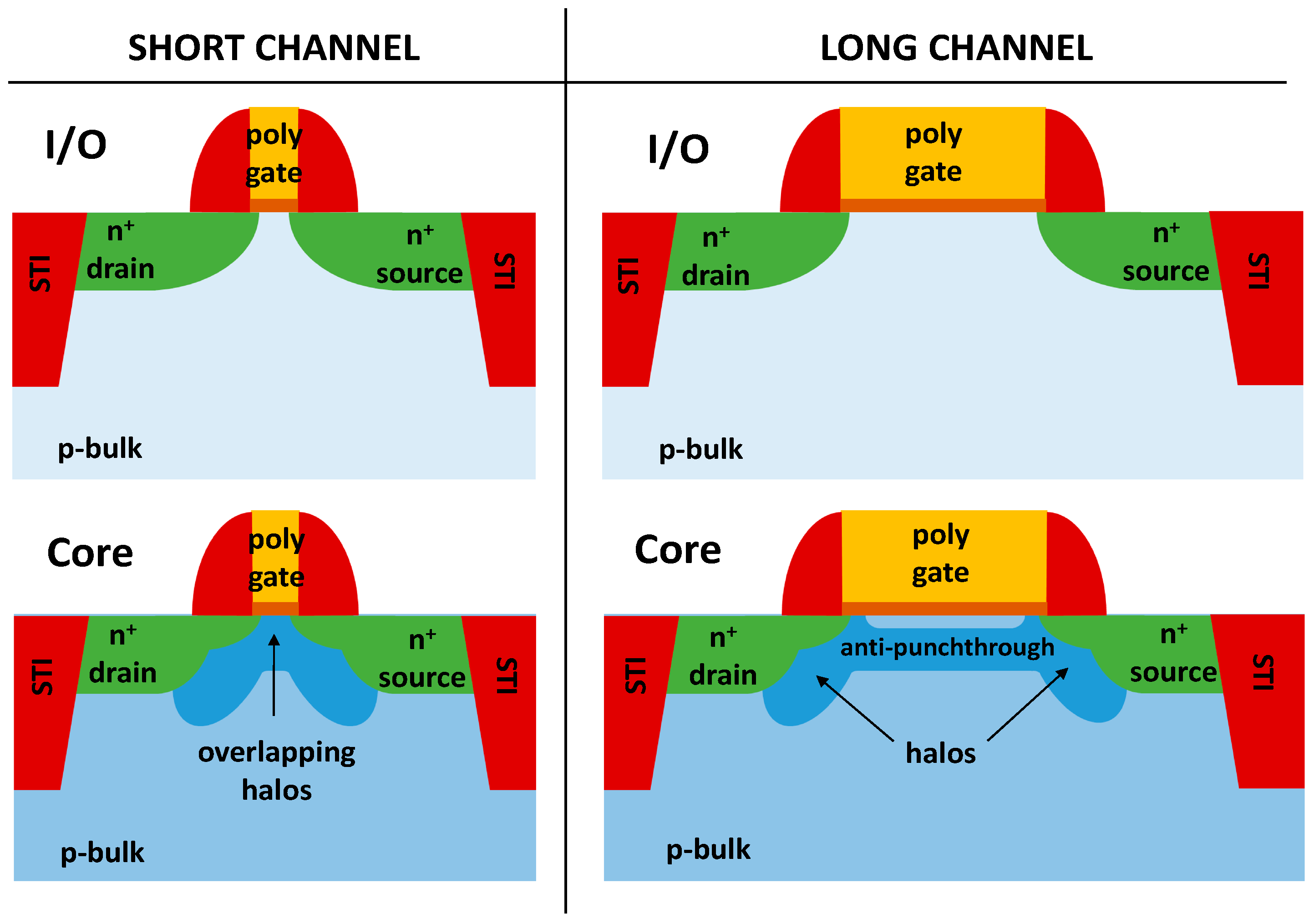
2.1. Test Structures
2.2. Exposure Conditions and Measurement Details
3. Experimental Results and Discussion
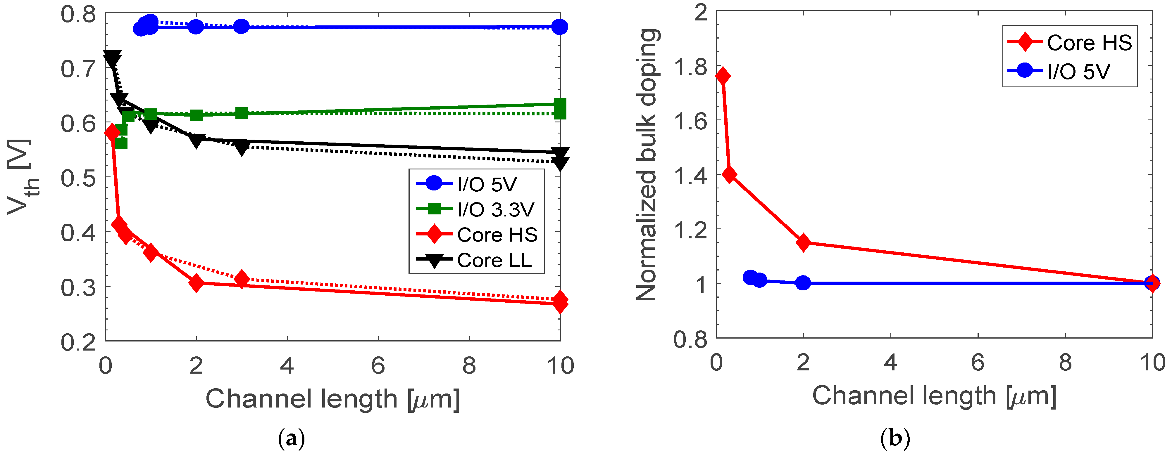
3.1. Bulk Doping
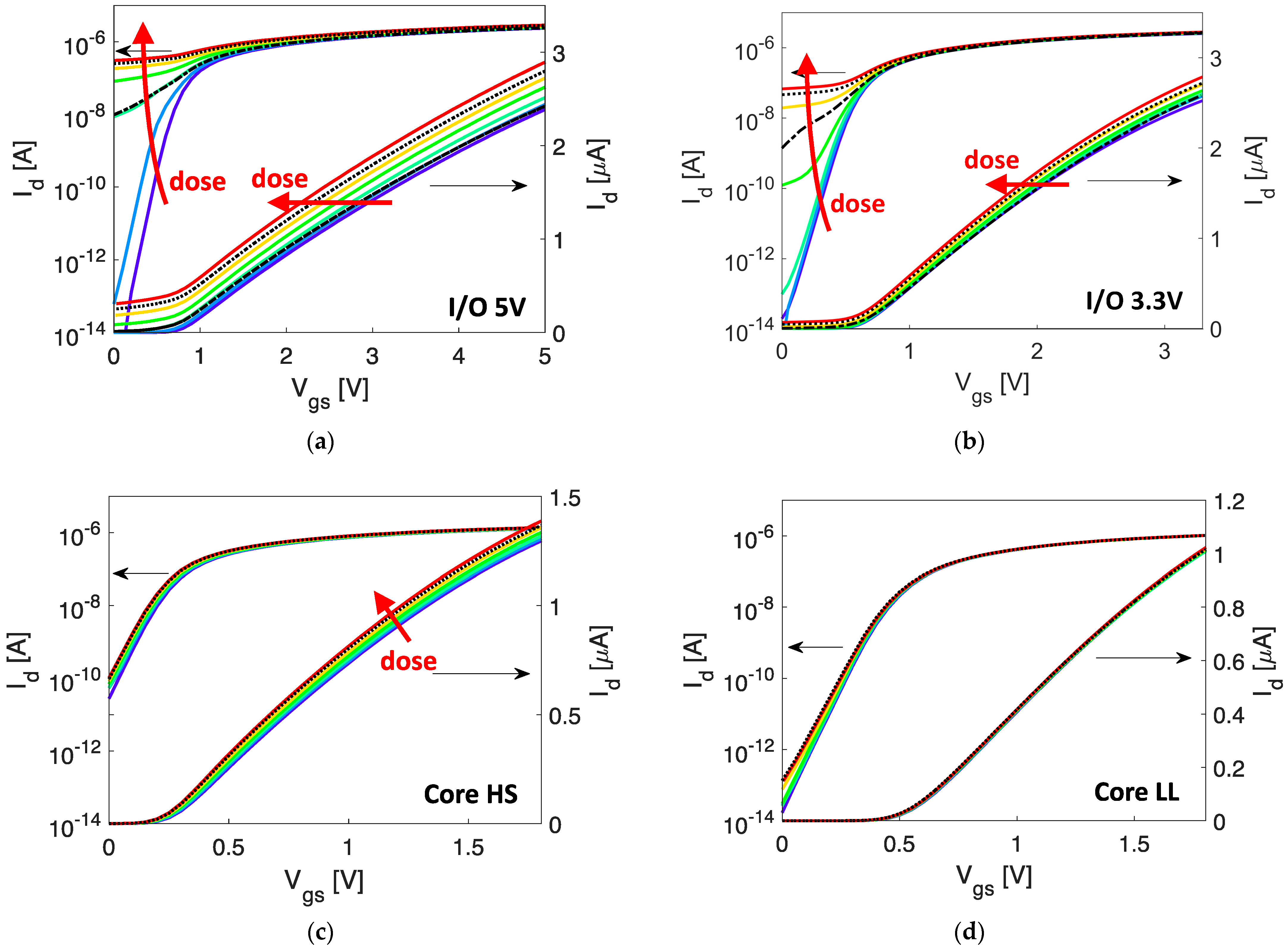
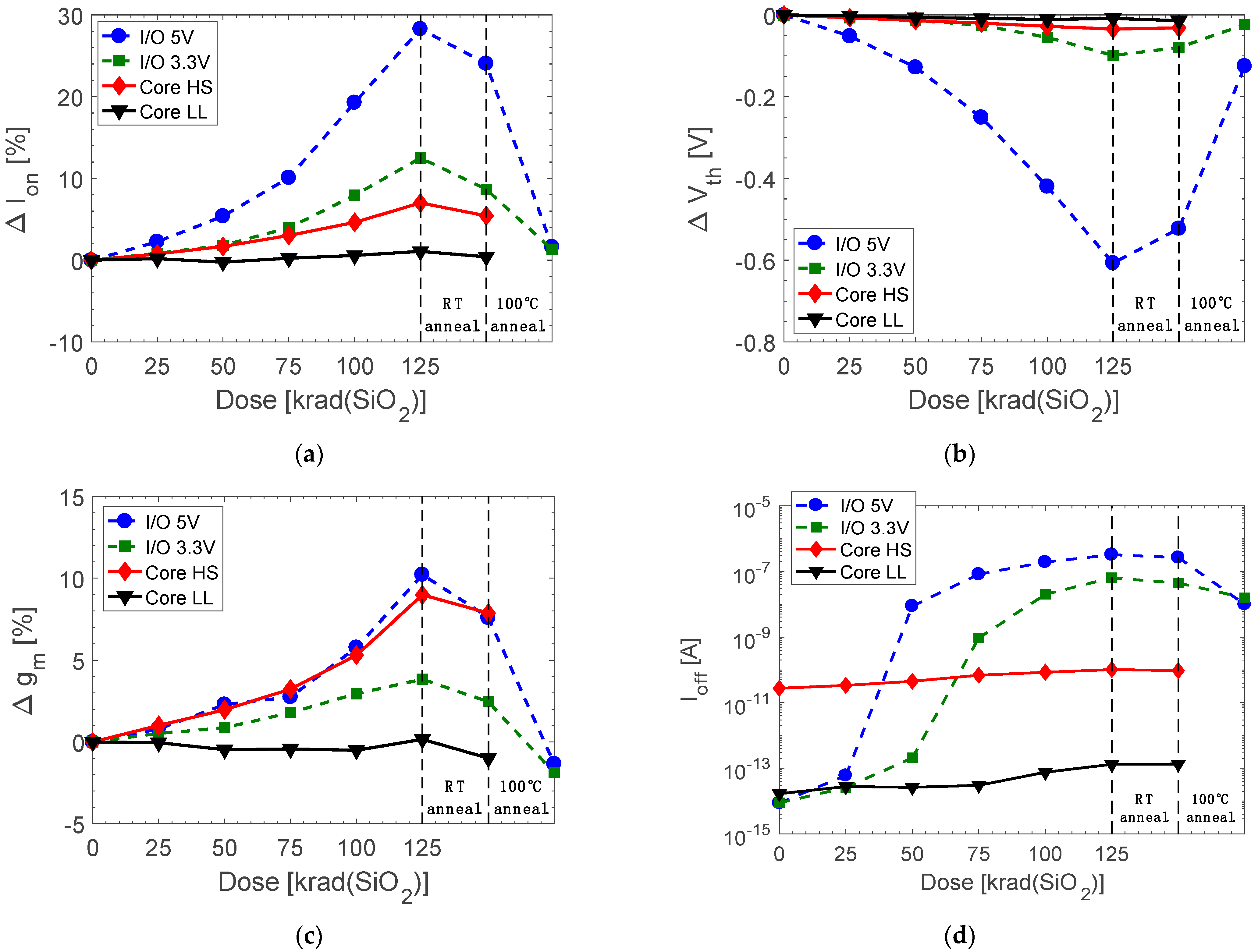
3.2. TID Effects on I/O and Core nMOSFETs
- -
- I/O transistors degrade more than core devices, mainly due to a large negative Vth shift and an increase in the subthreshold leakage current Ioff.
- -
- The TID degradation of core devices is modest and related to variations in gm.
- -
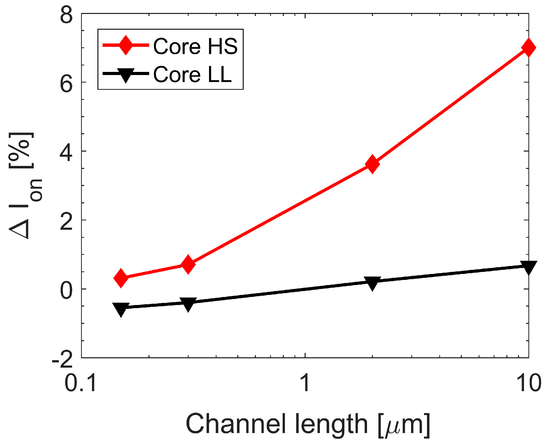
- Low-leakage (LL) core devices show a higher TID tolerance than that of high-speed (HS) core devices.
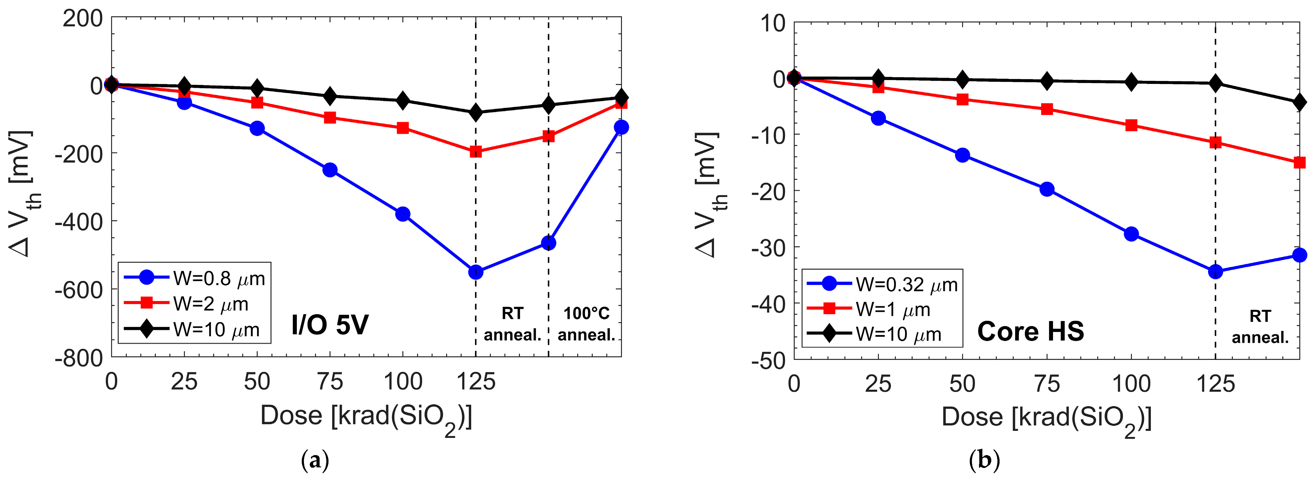
3.3. Channel-Width-Dependent Effects
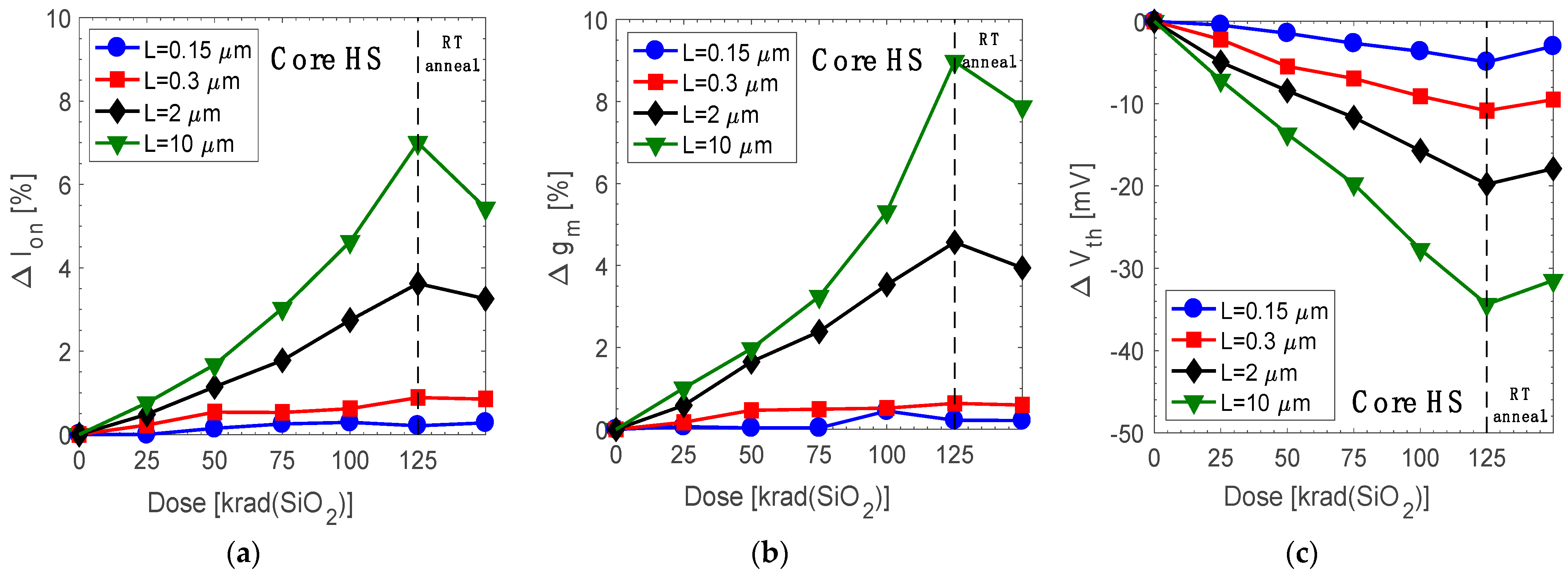
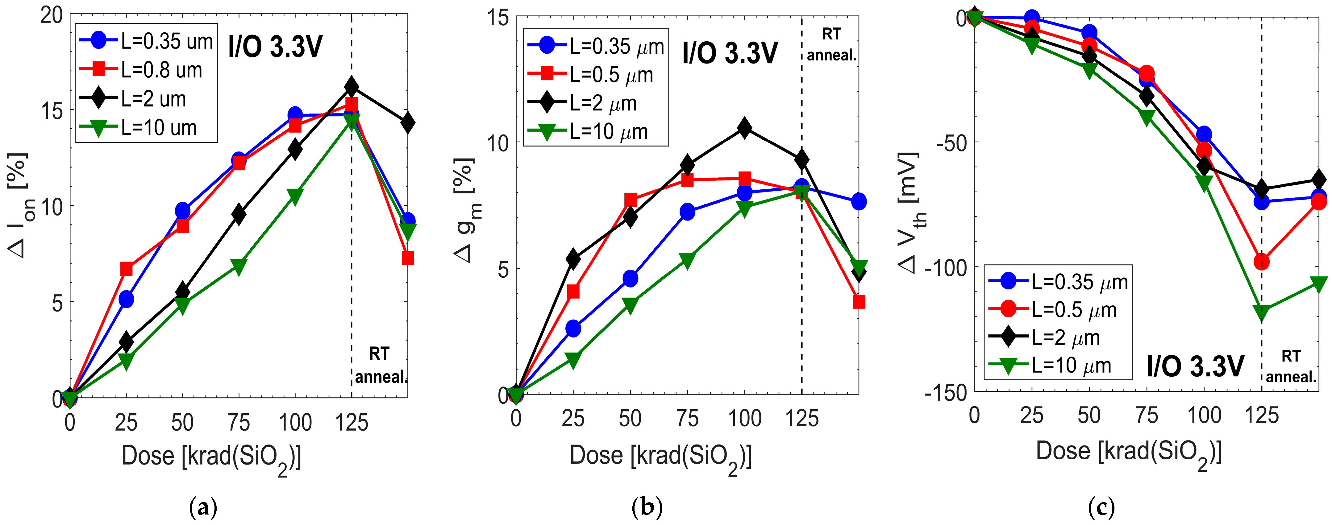
3.4. Channel-Length-Dependent Effects
4. Interpretation of Experimental Results
5. Conclusions
Author Contributions
Funding
Data Availability Statement
Acknowledgments
Conflicts of Interest
References
- Barth, J.L.; Dyer, C.S.; Stassinopoulos, E.G. Space, atmospheric, and terrestrial radiation environments. IEEE Trans. Nucl. Sci. 2003, 50, 466–482. [Google Scholar] [CrossRef]
- Schwank, J.R.; Shaneyfelt, M.R.; Dodd, P.E. Radiation hardness assurance testing of microelectronic devices and integrated circuits: Radiation environments, physical mechanisms, and foundations for hardness assurance. IEEE Trans. Nucl. Sci. 2013, 60, 2074–2100. [Google Scholar] [CrossRef]
- Barnaby, H.J. Total-ionizing-dose effects in modern CMOS technologies. IEEE Trans. Nucl. Sci. 2006, 53, 3103–3121. [Google Scholar] [CrossRef]
- Schwank, J.R. Radiation effects in MOS oxides. IEEE Trans. Nucl. Sci. 2008, 55, 1833–1853. [Google Scholar] [CrossRef]
- Fleetwood, D.M. Radiation Effects in a post-Moore word. IEEE Trans. Nucl. Sci. 2021, 68, 509–545. [Google Scholar] [CrossRef]
- Manghisoni, M.; Ratti, L.; Re, V.; Speziali, V.; Traversi, G.; Candelori, A. Comparison of ionizing radiation effects in 0.18 and 0.25 μm CMOS technologies for analog applications. IEEE Trans. Nucl. Sci. 2003, 50, 1827–1833. [Google Scholar] [CrossRef]
- Seo, D.; Trang, L.D.; Han, J.-W.; Kim, J.; Lee, J.; Lee, S.; Chang, I.-J. Total Ionizing Dose Effect on Ring Oscillator Frequency in 28-nm FD-SOI Technology. IEEE Electron. Device Lett. 2018, 39, 1728–1731. [Google Scholar] [CrossRef]
- Ma, T.; Bonaldo, S.; Mattiazzo, S.; Baschirotto, A.; Enz, C.; Paccagnella, A.; Gerardin, S. TID degradation mechanisms in 16-nm bulk FinFETs irradiated to ultrahigh doses. IEEE Trans. Nucl. Sci. 2021, 68, 1571–1578. [Google Scholar] [CrossRef]
- Gorchichko, M.; Zhang, E.X.; Wang, P.; Bonaldo, S.; Schrimpf, R.D.; Reed, R.A.; Linten, D.; Mitard, J.; Fleetwood, D.M. Total-ionizing-dose response of highly scaled gate-all-around Si nanowire CMOS transistors. IEEE Trans. Nucl. Sci. 2021, 68, 687–696. [Google Scholar] [CrossRef]
- Bonaldo, S.; Gorchichko, M.; Zhang, E.X.; Ma, T.; Matiazzo, S.; Bagatin, M.; Paccagnella, A.; Gerardin, S.; Schrimpf, R.D.; Reed, R.A.; et al. TID effects in highly scaled gate-all-around Si nanowire CMOS transistors irradiated to ultrahigh doses. IEEE Trans. Nucl. Sci. 2022, 69, 1444–1452. [Google Scholar] [CrossRef]
- Benedetto, J.M.; Boesch, H.E.; McLean, F.B.; Mize, J.P. Hole removal in thin-gate MOSFETs by tunneling. IEEE Trans. Nucl. Sci. 1985, 2, 3916–3920. [Google Scholar] [CrossRef]
- Fleetwood, D.M. ’Border traps’ in MOS devices. IEEE Trans. Nucl. Sci. 1992, 39, 269–271. [Google Scholar] [CrossRef]
- Fleetwood, D.M.; Winokur, P.S.; Reber, R.A., Jr.; Meisenheimer, T.L.; Schwank, J.R.; Shaneyfelt, M.R.; Riewe, L.C. Effects of oxide traps, interface traps, and “border traps” on metal-oxide-semiconductor devices. J. Appl. Phys. 1993, 73, 5058. [Google Scholar] [CrossRef]
- Ajayan, J.; Nirmal, D.; Tayal, S.; Bhattacharya, S.; Arivazhagan, L.; Augustine Fletcher, A.S.; Murugapandiyan, P.; Ajitha, D. Nanosheet field effect transistors-A next generation device to keep Moore’s law alive: An intensive study. Microelectron. J. 2021, 114, 105141. [Google Scholar] [CrossRef]
- Gaillardin, M.; Goiffon, V.; Girard, S.; Martinez, M.; Magnan, P.; Paillet, P. Enhanced radiation-induced narrow channel effects in commercial 0.18 μm bulk technology. IEEE Trans. Nucl. Sci. 2011, 58, 2807–2815. [Google Scholar] [CrossRef]
- Faccio, F.; Michelis, S.; Cornale, D.; Paccagnella, A.; Gerardin, S. Radiation-induced short channel (RISCE) and narrow channel (RINCE) effects in 65 and 130 nm MOSFETs. IEEE Trans. Nucl. Sci. 2015, 62, 2933–2940. [Google Scholar] [CrossRef]
- Chatterjee, I.; Zhang, E.X.; Bhuva, B.L.; Reed, R.A.; Alles, M.L.; Mahatme, N.N.; Ball, D.R.; Schrimpf, R.D.; Fleetwood, D.M.; Linten, D.; et al. Geometry Dependence of Total-Dose Effects in Bulk FinFETs. IEEE Trans. Nucl. Sci. 2014, 61, 2951–2958. [Google Scholar] [CrossRef]
- Bonaldo, S.; Ma, T.; Mattiazzo, S.; Baschirotto, A.; Enz, C.; Fleetwood, D.M.; Paccagnella, A.; Gerardin, S. DC response, low-frequency noise, and TID-induced mechanisms in 16-nm FinFETs for high-energy physics experiments. Nucl. Instrum. Methods. Phys. Res. B. 2022, 1033, 166727. [Google Scholar] [CrossRef]
- Bonaldo, S.; Zhao, S.E.; O’Hara, A.; Gorchichko, M.; Zhang, E.X.; Gerardin, S.; Paccagnella, A.; Waldron, N.; Collaert, N.; Putcha, V.; et al. Total-ionizing-dose effects and low-frequency noise in 16-nm InGaAs FinFETs with HfO2/Al2O3 dielectrics. IEEE Trans. Nucl. Sci. 2019, 67, 210–220. [Google Scholar] [CrossRef]
- Zhao, S.E.; Bonaldo, S.; Wang, P.; Zhang, E.X.; Waldron, N.; Collaert, N.; Putcha, V.; Linten, D.; Gerardin, S.; Paccagnella, A.; et al. Total-ionizing-dose effects on InGaAs FinFETs with modified gate-stack. IEEE Trans. Nucl. Sci. 2019, 67, 253–259. [Google Scholar] [CrossRef]
- Duan, G.X.; Zhang, C.X.; Zhang, E.X.; Hachtel, J.; Fleetwood, D.M.; Schrimpf, R.D.; Reed, R.A.; Alles, M.L.; Pantelides, S.T.; Bersuker, G.; et al. Bias Dependence of Total Ionizing Dose Effects in SiGe-MOS FinFETs. IEEE Trans. Nucl. Sci. 2014, 61, 2834–2838. [Google Scholar] [CrossRef]
- Faccio, F.; Cervelli, G. Radiation-induced edge effects in deep submicron CMOS transistors. IEEE Trans. Nucl. Sci. 2005, 52, 2413–2420. [Google Scholar] [CrossRef]
- Xi, S.; Zheng, Q.; Lu, W.; Cui, J.; Wei, Y.; Guo, Q. Modelling of TID-induced leakage current in ultra-deep submicron SOI NMOSFETs. Microelectron. J. 2020, 102, 104829. [Google Scholar] [CrossRef]
- Shaneyfelt, M.R.; Dodd, P.E.; Draper, B.L.; Flores, R.S. Challenges in hardening technologies using shallow-trench isolation. IEEE Trans. Nucl. Sci. 1998, 45, 2584–2592. [Google Scholar] [CrossRef]
- McLain, M.L.; Barnaby, H.J.; Schlenvogt, G. Effects of channel implant variation on radiation-induced edge leakage currents in n-Channel MOSFETs. IEEE Trans. Nucl. Sci. 2017, 64, 2235–2241. [Google Scholar] [CrossRef]
- Gerardin, S.; Gasperin, A.; Cester, A.; Paccagnella, A.; Ghidini, G.; Candelori, A.; Bacchetta, N.; Bisello, D.; Glaser, M. Impact of 24-GeV proton irradiation on m CMOS devices. IEEE Trans. Nucl. Sci. 2006, 53, 1917–1922. [Google Scholar] [CrossRef]
- Faccio, F.; Borghello, G.; Lerario, E.; Fleetwood, D.M.; Schrimpf, R.D.; Gong, H.; Zhang, E.X.; Wag, P.; Michelis, S.; Geradin, S.; et al. Influence of LDD spacers and H+ transport on the total-ionizing-dose response of 65-nm MOSFETs irradiated to ultrahigh doses. IEEE Trans. Nucl. Sci. 2018, 65, 164–174. [Google Scholar] [CrossRef]
- Bonaldo, S.; Gerardin, S.; Jin, X.; Paccagnella, A.; Faccio, F.; Borghello, G.; Fleetwood, D. Charge buildup and spatial distribution of interface traps in 65 nm pMOSFETs irradiated to ultra-high Doses. IEEE Trans. Nucl. Sci. 2019, 66, 1574–1583. [Google Scholar] [CrossRef]
- Arora, R.; Simoen, E.; Zhang, E.X.; Fleetwood, D.M.; Schrimpf, R.D.; Galloway, K.F.; Choi, B.K.; Mitard, J.; Meuris, M.; Claeys, C.; et al. Effects of halo doping and Si capping layer thickness on total-dose effects in Ge p-MOSFETs. IEEE Trans. Nucl. Sci. 2010, 57, 1933–1939. [Google Scholar] [CrossRef]
- Esqueda, I.S.; Barnaby, H.J.; Alles, M.L. Two-dimensional methodology for modeling radiation-induced off-state leakage in CMOS technologies. IEEE Trans. Nucl. Sci. 2005, 52, 2259–2264. [Google Scholar] [CrossRef]
- Bonaldo, S.; Mattiazzo, S.; Enz, C.; Baschirotto, A.; Fleetwood, D.M.; Paccagnella, A.; Gerardin, S. Ionizing-radiation response and low-frequency noise of 28-nm MOSFETs at ultrahigh doses. IEEE Trans. Nucl. Sci. 2020, 67, 1302–1311. [Google Scholar] [CrossRef]
- Rezzak, N.; Alles, M.L.; Schrimpf, R.D.; Kalemeris, S.; Massengill, L.W.; Sochacki, J.; Barnaby, H.J. The sensitivity of radiation-induced leakage to STI topology and sidewall doping. Microel. Rel. 2011, 51, 889–894. [Google Scholar] [CrossRef]
- Bonaldo, S.; Mattiazzo, S.; Enz, C.; Baschirotto, A.; Paccagnella, A.; Jin, X.; Gerardin, S. Influence of halo implantations on the total ionizing dose response of 28-nm pMOSFETs irradiated to ultrahigh doses. IEEE Trans. Nucl. Sci. 2019, 66, 82–90. [Google Scholar] [CrossRef]
- Bisello, D.; Candelori, A.; Kaminski, A.; Litovchenko, A.; Noah, E.; Stefanutti, L. X-ray radiation source for total dose radiation studies. Rad. Phys. Chem. 2004, 71, 713–715. [Google Scholar] [CrossRef]
- Total Dose Steady-State Irradiation Test Method. ESCC Basic Specification No. 22900, No. 5, European Space Agency. June 2016. Available online: http://escies.org/escc-specs/published/22900.pdf (accessed on 28 December 2022).
- Dressendorfer, P.V.; Soden, J.M.; Harrington, J.J.; Nordstrom, T.V. The effects of test conditions on MOS radiation-hardness results. IEEE Trans. Nucl. Sci. 1981, 28, 4281–4287. [Google Scholar] [CrossRef]
- Winokur, P.S.; Schwank, J.R.; McWhorter, P.J.; Dressendorfer, P.V.; Turpin, D.C. Correlating the Radiation Response of MOS Capacitors and Transistors. IEEE Trans. Nucl. Sci. 1984, 31, 1453–1460. [Google Scholar] [CrossRef]
- Johnson, A.H.; Swimm, R.T.; Thorbourn, D.O.; Adell, P.C.; Rax, B.G. Field dependence of charge yield in silicon dioxide. IEEE Trans. Nucl. Sci. 2014, 61, 2818–2825. [Google Scholar] [CrossRef]
- Borse, D.G.; Rani KN, M.; Jha, N.K.; Chandorkar, A.N.; Vasi, J.; Ramgopal Rao, V.; Cheng, B.; Woo, J.C.S. Optimization and realization of sub-100-nm channel length single halo p-MOSFETs. IEEE Trans. Nucl. Sci. 2002, 49, 1077–1079. [Google Scholar] [CrossRef]
- Rios, R.; Shih, W.K.; Shah, A.; Mudanai, S.; Packan, P.; Sandford, T.; Mistry, K. A three-transistor threshold voltage model for halo processes. In Proceedings of the International Electron Devices Meeting, San Francisco, CA, USA, 8–11 December 2002; pp. 113–116. [Google Scholar]
- Meer, H.; Henson, K.; Lyu, J.; Rosmeulen, M.; Kubicek, S.; Collaert, N.; De Meyer, K. Limitations of shift-and-ratio based Leff extraction techniques for MOS transistors with halo or pocket implants. IEEE Elec. Dev. Let. 2000, 21, 133–136. [Google Scholar] [CrossRef]
- Kunikiyo, T.; Mitsui, K.; Fujinaga, M.; Uchida, T.; Kotani, N. Reverse short-channel effect due to lateral diffusion of point-defect induced by source/drain ion implantation. IEEE Trans. Comput. Aided Des. Integr. Circuits Syst. 1994, 13, 507–514. [Google Scholar] [CrossRef]
- Turowski, M.; Raman, A.; Schrimpf, R. Nonuniform total-dose induced charge distribution in shallow-trench isolation oxides. IEEE Trans. Nucl. Sci. A 2004, 51, 3166–3171. [Google Scholar] [CrossRef]


| MOSFET Type | #1 Narrow/Short W/L [μm] | #2 Narrow/Long W/L [μm] | #3 Large/Long W/L [μm] |
|---|---|---|---|
| I/O 5V nMOSFET | 0.8/0.8 | 0.8/10 | 10/10 |
| I/O 3.3V nMOSFET | 0.8/0.35 | 0.8/10 | 10/10 |
| Core HS 1.8V nMOSFET | 0.32/0.15 | 0.32/10 | 10/10 |
| Core LL 1.8V nMOSFET | 0.32/0.15 | 0.32/10 | 10/10 |
Disclaimer/Publisher’s Note: The statements, opinions and data contained in all publications are solely those of the individual author(s) and contributor(s) and not of MDPI and/or the editor(s). MDPI and/or the editor(s) disclaim responsibility for any injury to people or property resulting from any ideas, methods, instructions or products referred to in the content. |
© 2023 by the authors. Licensee MDPI, Basel, Switzerland. This article is an open access article distributed under the terms and conditions of the Creative Commons Attribution (CC BY) license (https://creativecommons.org/licenses/by/4.0/).
Share and Cite
Bonaldo, S.; Mattiazzo, S.; Bagatin, M.; Paccagnella, A.; Margutti, G.; Gerardin, S. Influence of Bulk Doping and Halos on the TID Response of I/O and Core 150 nm nMOSFETs. Electronics 2023, 12, 543. https://doi.org/10.3390/electronics12030543
Bonaldo S, Mattiazzo S, Bagatin M, Paccagnella A, Margutti G, Gerardin S. Influence of Bulk Doping and Halos on the TID Response of I/O and Core 150 nm nMOSFETs. Electronics. 2023; 12(3):543. https://doi.org/10.3390/electronics12030543
Chicago/Turabian StyleBonaldo, Stefano, Serena Mattiazzo, Marta Bagatin, Alessandro Paccagnella, Giovanni Margutti, and Simone Gerardin. 2023. "Influence of Bulk Doping and Halos on the TID Response of I/O and Core 150 nm nMOSFETs" Electronics 12, no. 3: 543. https://doi.org/10.3390/electronics12030543
APA StyleBonaldo, S., Mattiazzo, S., Bagatin, M., Paccagnella, A., Margutti, G., & Gerardin, S. (2023). Influence of Bulk Doping and Halos on the TID Response of I/O and Core 150 nm nMOSFETs. Electronics, 12(3), 543. https://doi.org/10.3390/electronics12030543