
Dynamic Dead-Time Compensation Method Based on Switching Characteristics of the MOSFET for PMSM Drive System


Abstract
:1. Introduction
- The influence of the dead-time effect on motor drives is analyzed in detail, which manifests that the voltage deviation between voltage command and output voltage is the origin of the dead-time effect. As a result, the compensation principle can be established.
- The switching process of the power MOSFET is analyzed, especially the normal turn-off process and the QZCS turn-off process, which demonstrates that the switching time of the MOSFET varies with the load current and cannot be considered constant. In addition, the multipulse test (MPT) and the switching time of the MOSFET can be obtained accordingly. With the MPT result, the dynamic compensation method can be realized based on the lookup table and linear interpolation.
2. Impact of the Dead-Time Effect on Motor Drives
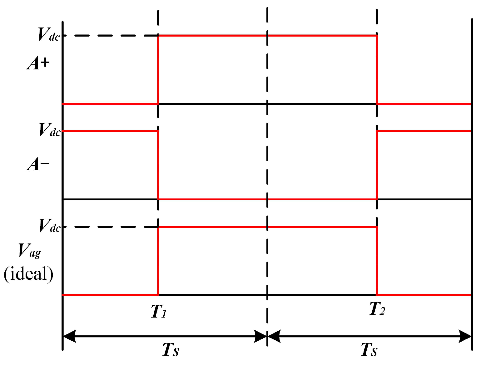
2.1. Ideal Condition (without Consideration of )
2.2. Actual Condition (with Consideration of )
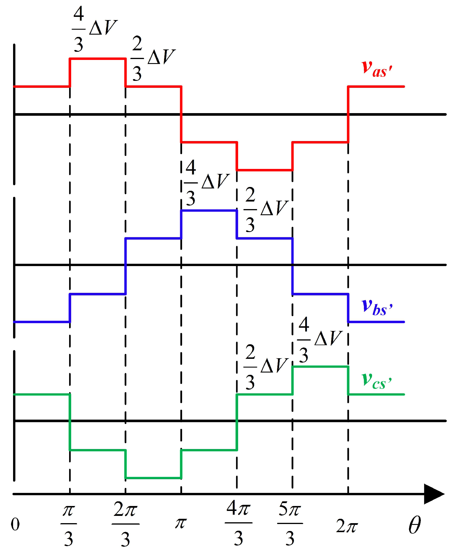
2.3. Impact of the Dead-Time Effect
2.4. Basic Principle of the Dead-Time Effect Compensation
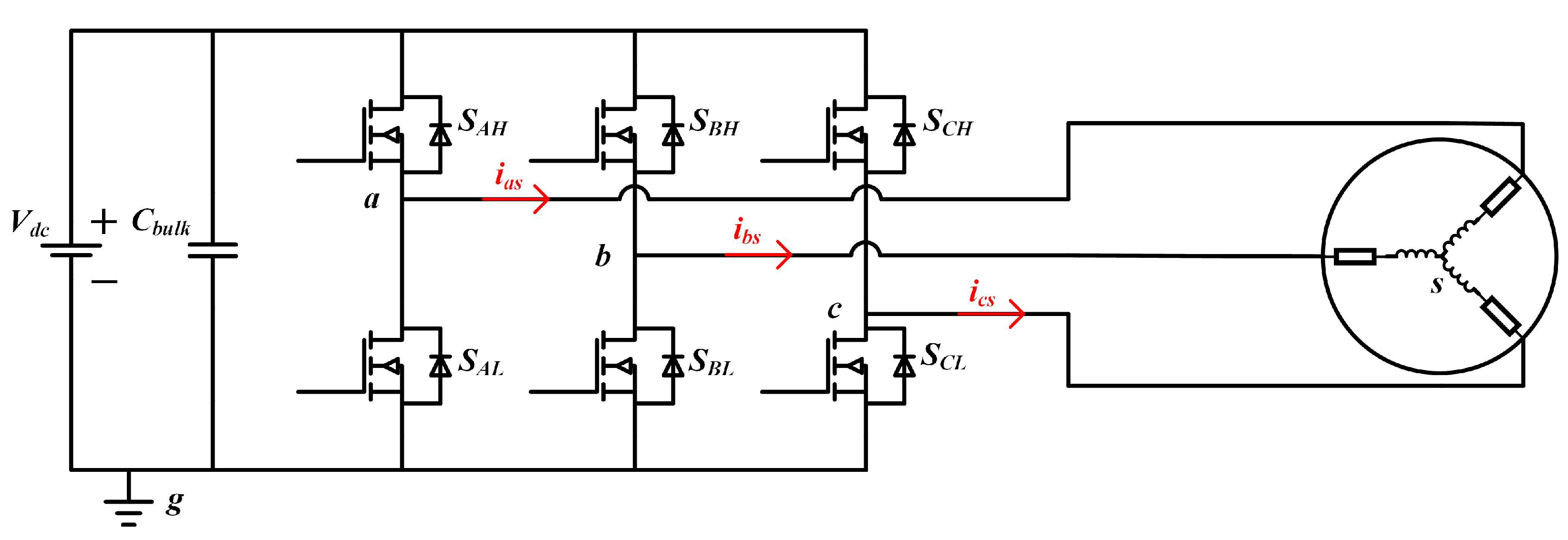
3. Switching Process of the Power MOSFET
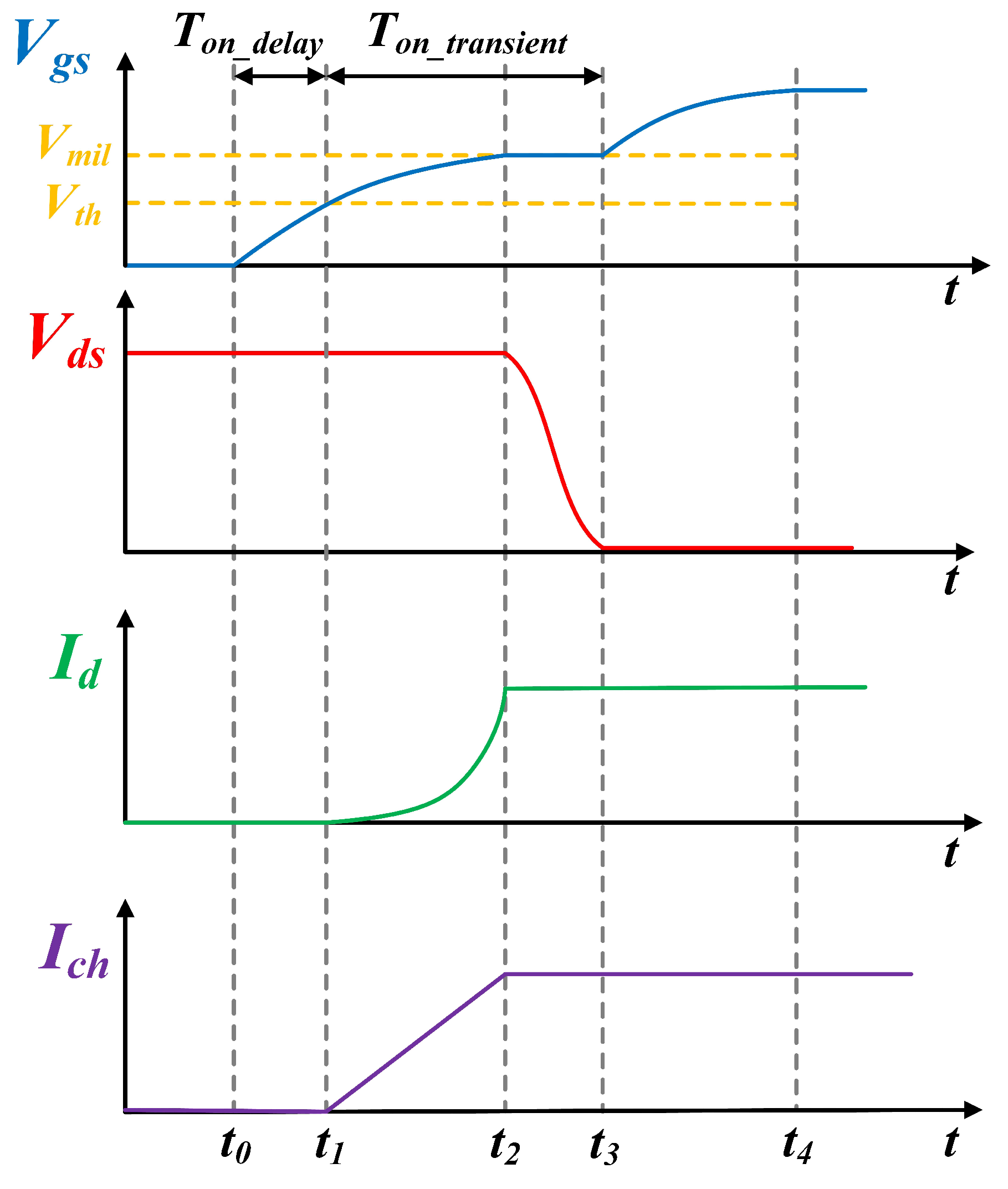
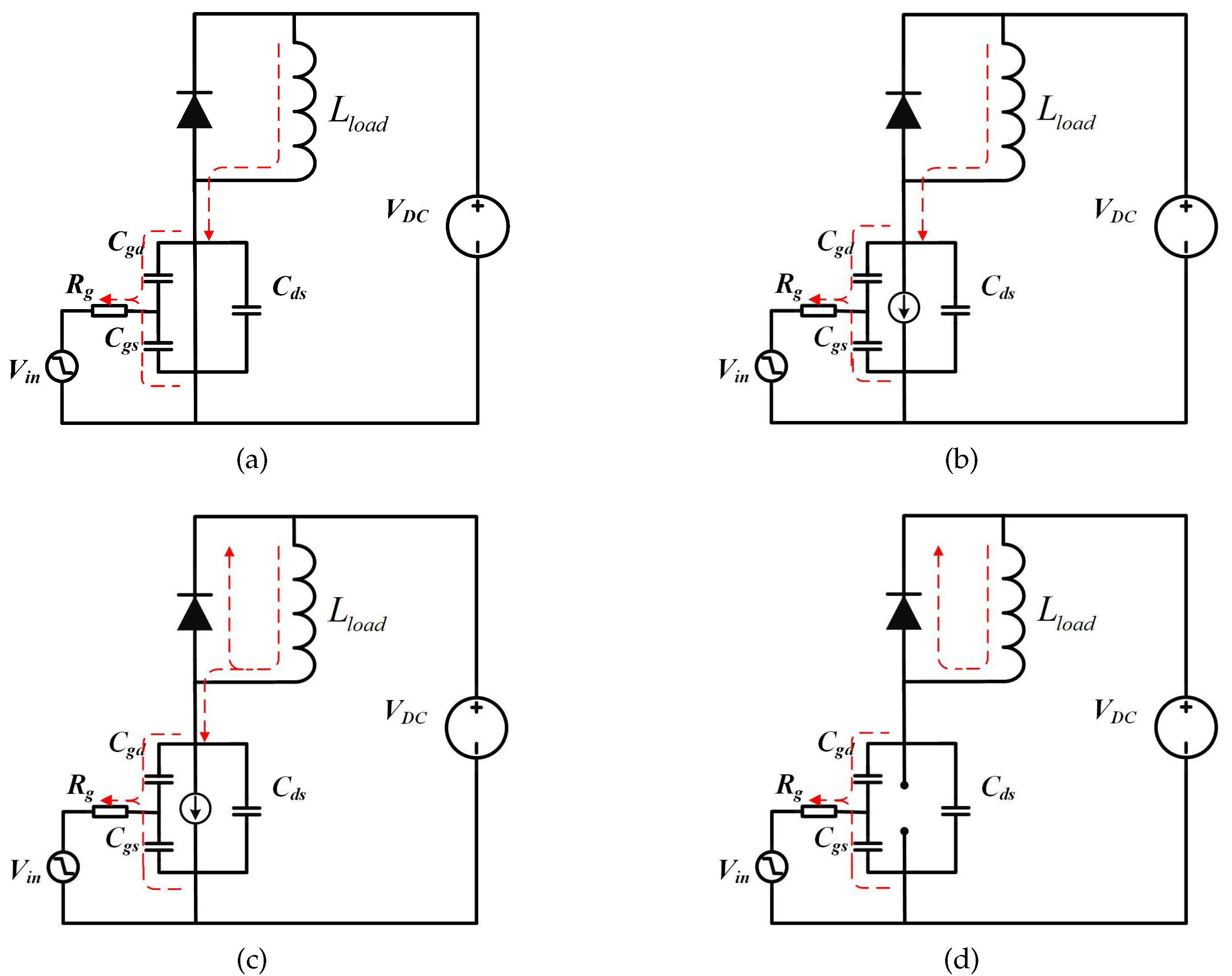
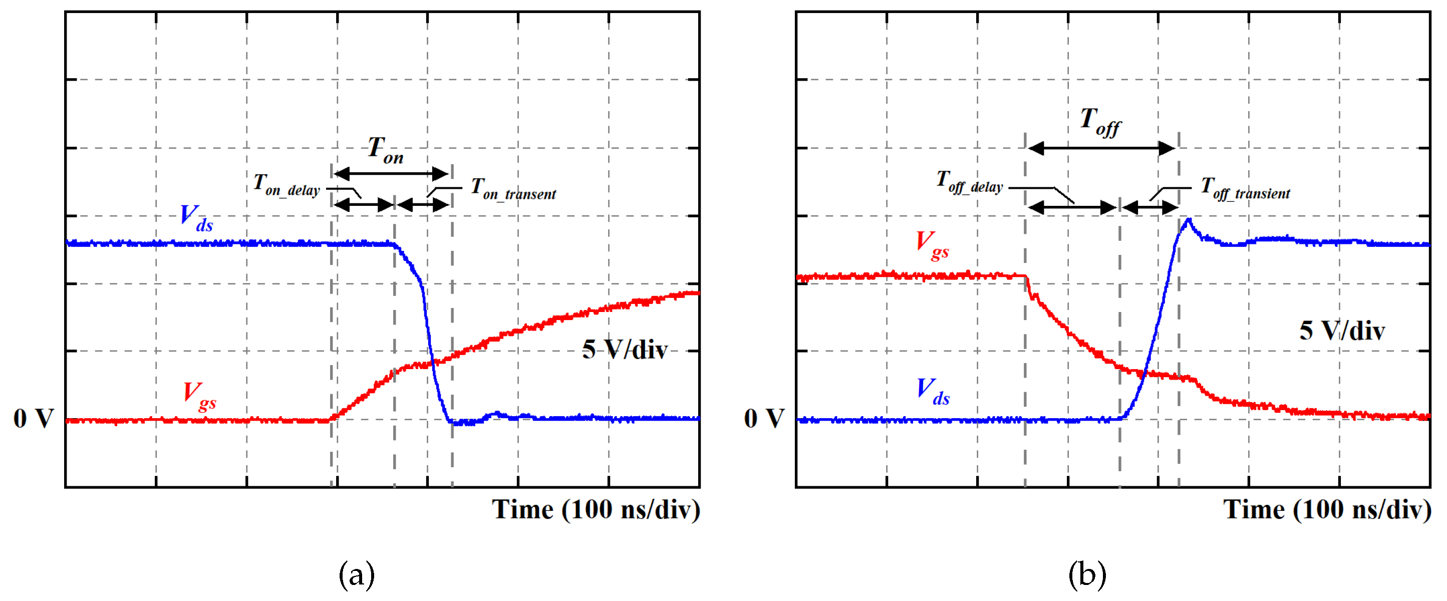
3.1. Turn-On Transition
3.2. Turn-Off Process
3.2.1. Normal Case
3.2.2. QZCS Case
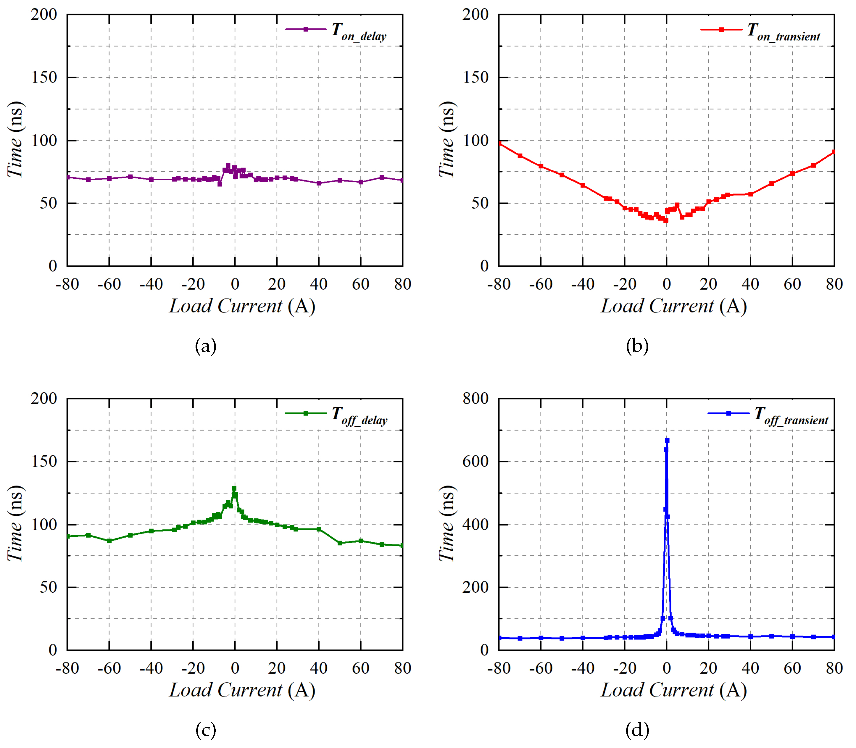
3.3. Relationships between / and Load Current
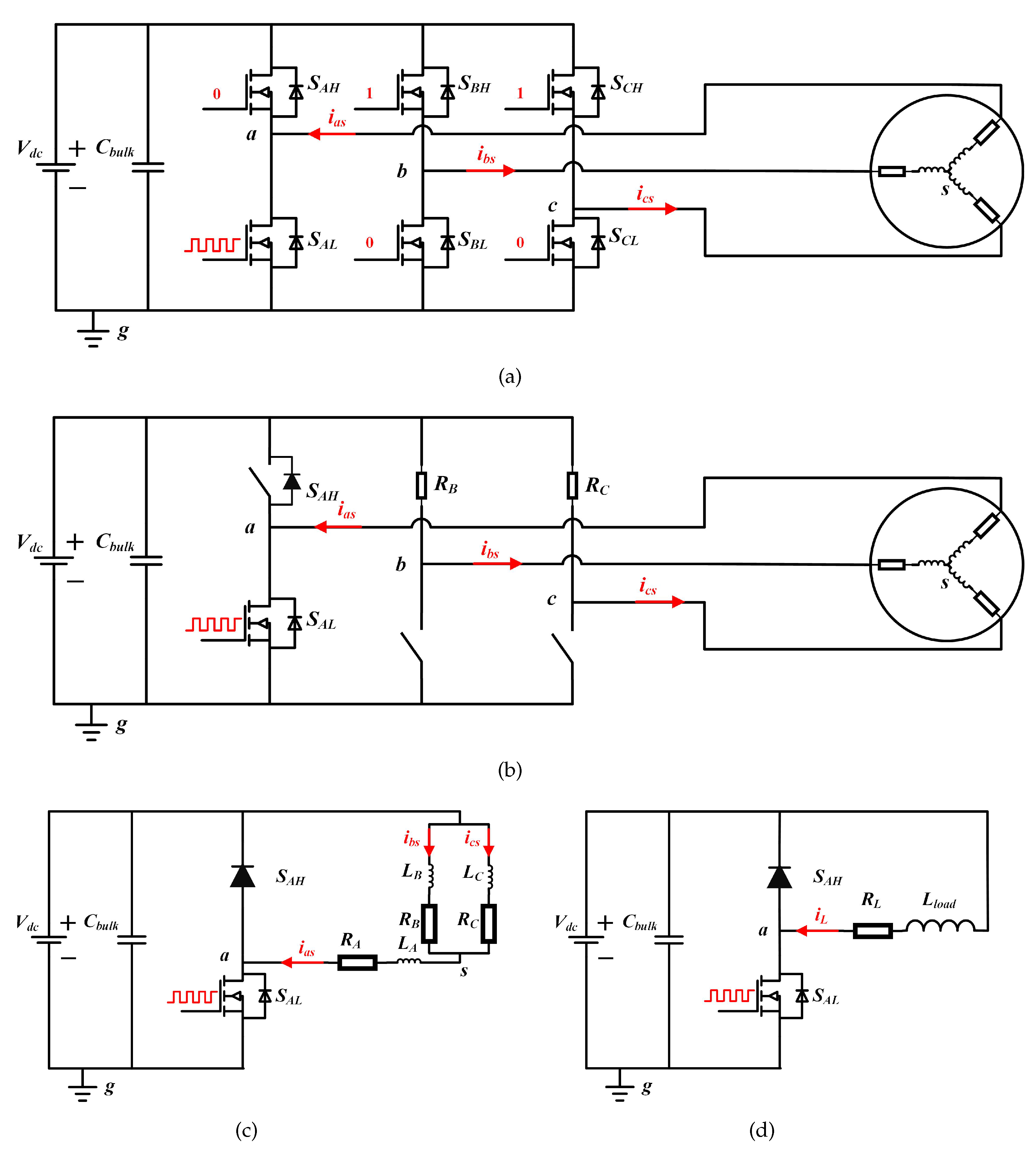
4. Switching Characteristic Evaluation of the MOSFET Based on the Multipulse Test
4.1. Principle of the MPT
4.2. Test Results of MPT
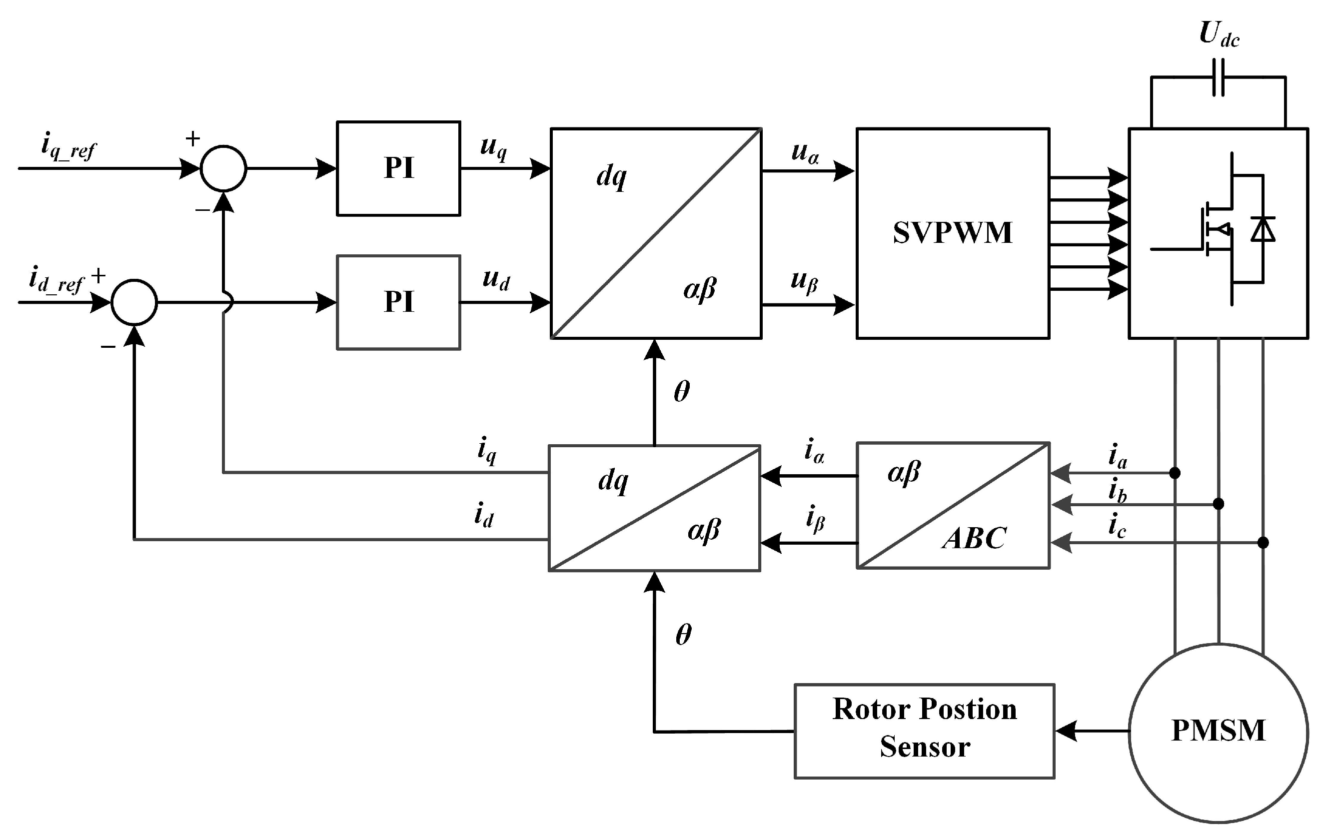
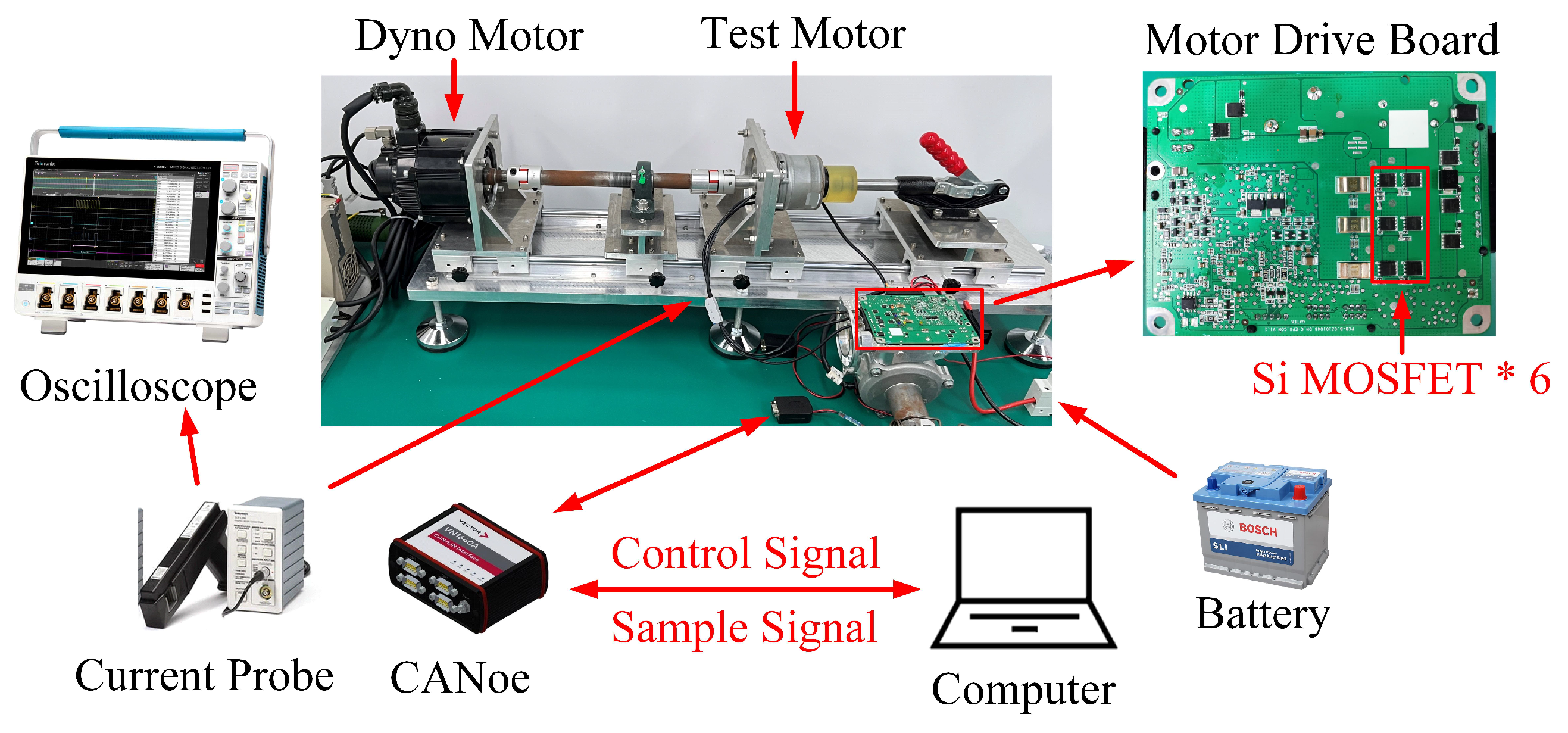
5. Experiment Verification
5.1. Experiment Bench
5.2. Experiment Results
6. Conclusions
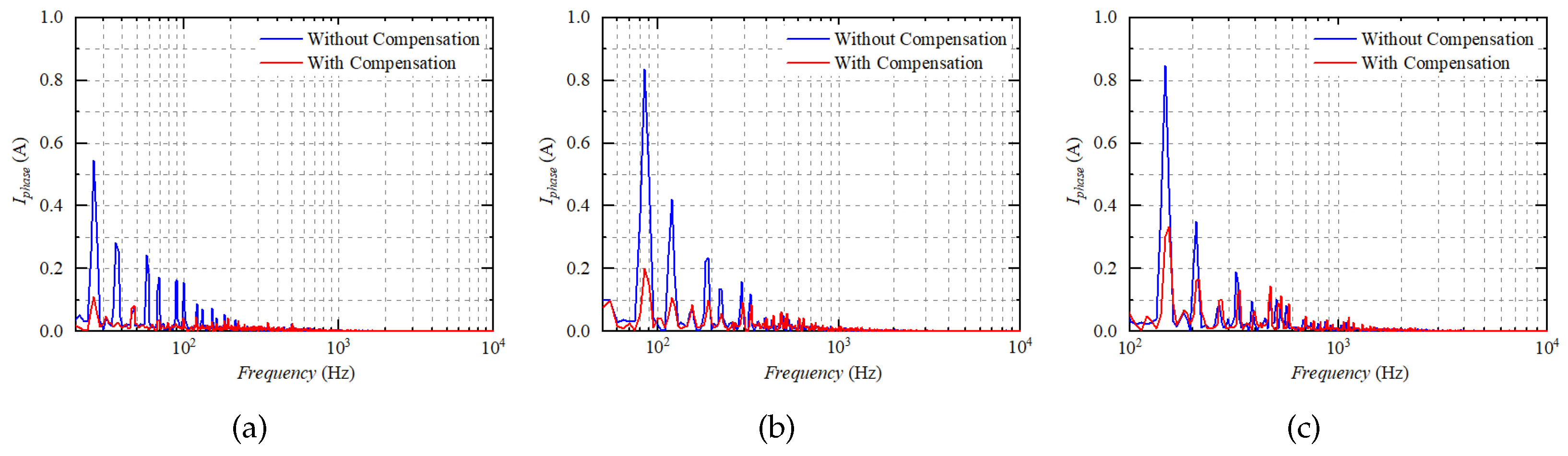
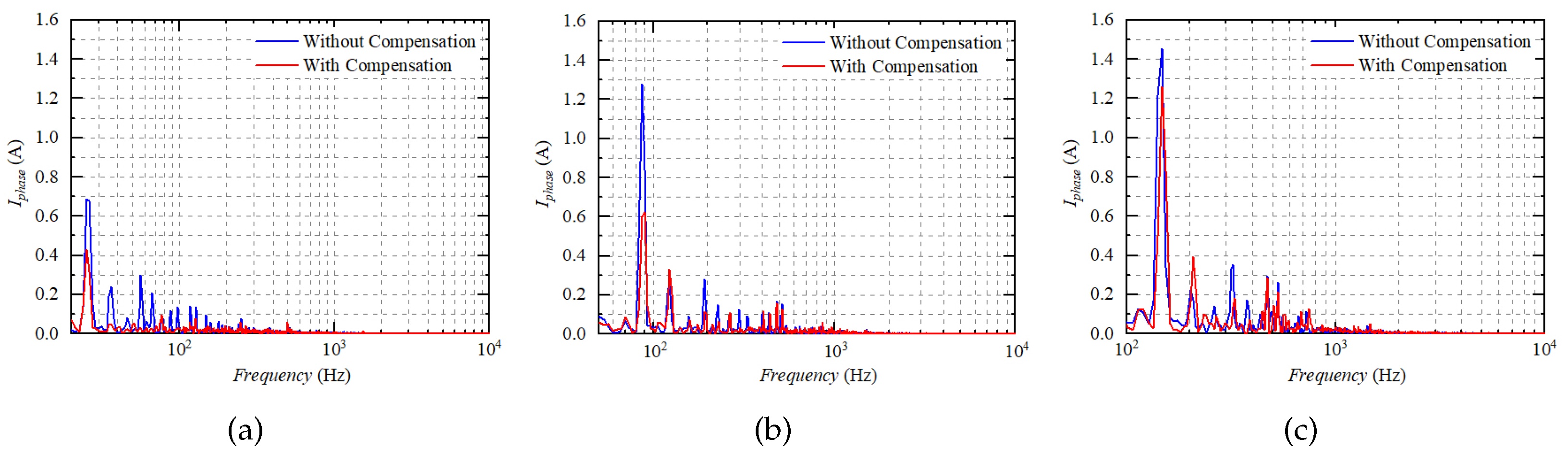
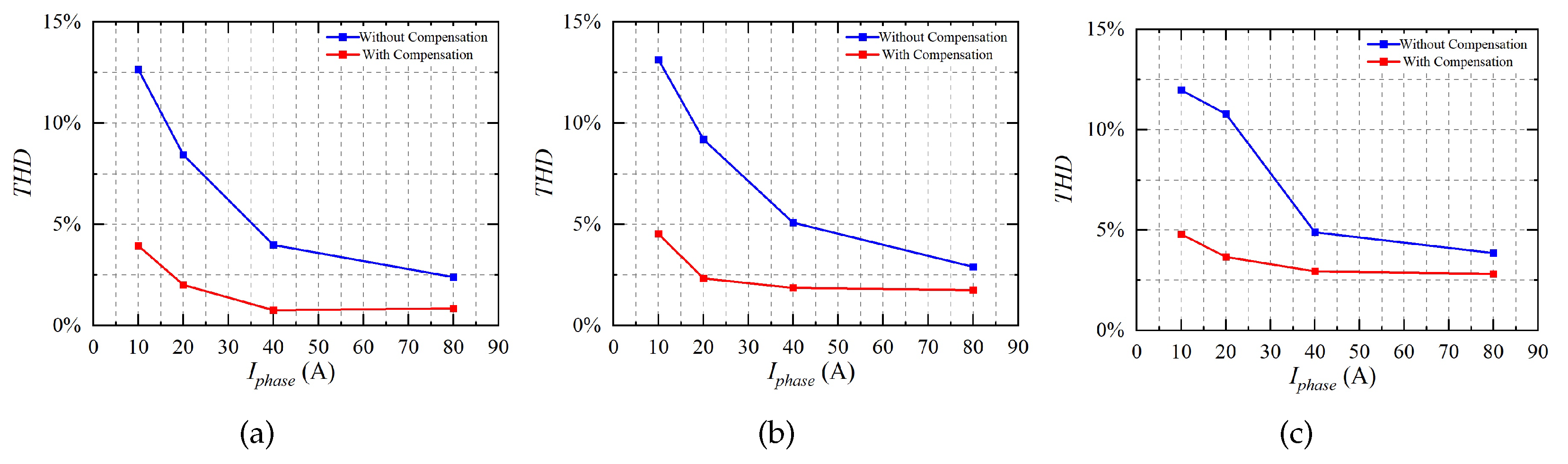
- The proposed compensation method shows a perfect performance in current distortion suppression with a low modulation index. With the increased modulation index, the dead-time effect is reduced, which makes the suppression of the current distortion not apparent;
- The proposed compensation method reduces the 5th-, 7th-, and 11th-order harmonics significantly in the low modulation index region, as well as the THD values. However, the reduction ratio of the harmonics and the THD values degrades with the increased modulation index, which can mainly be attributed to the harmonic characteristics of the SVPWM strategy adopted in the motor drives;
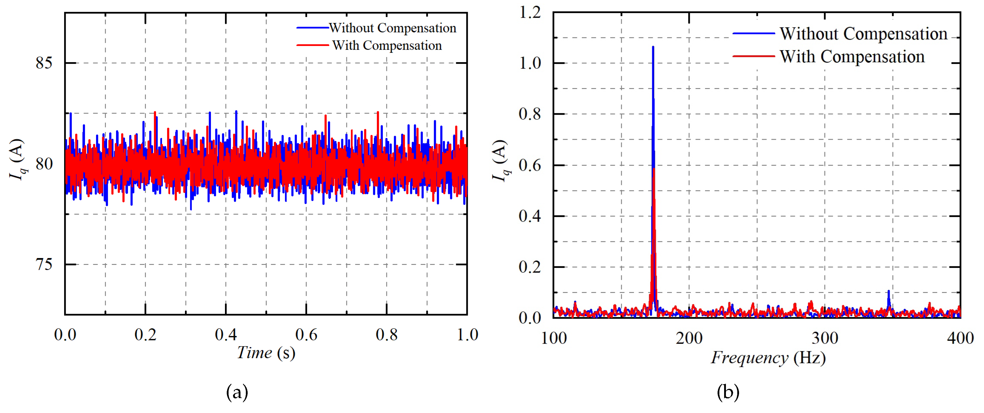
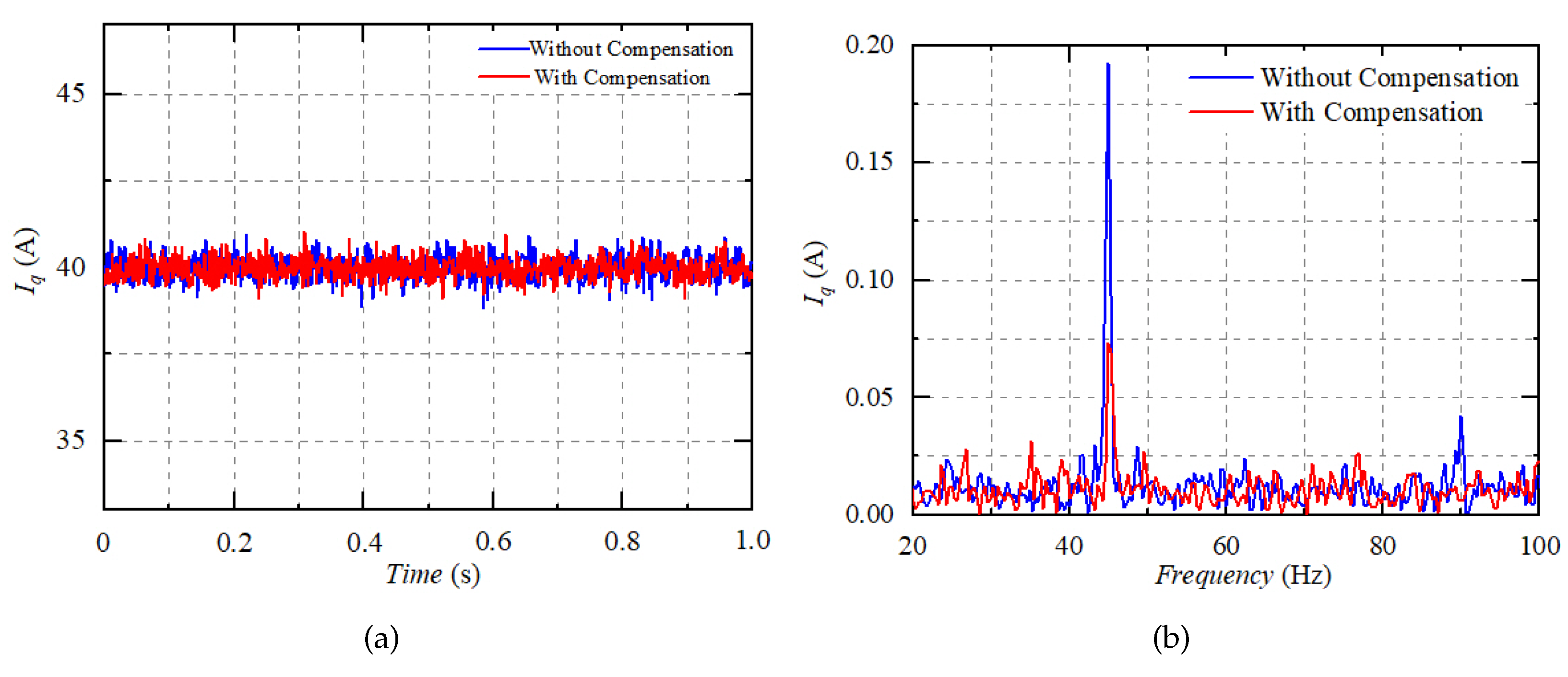
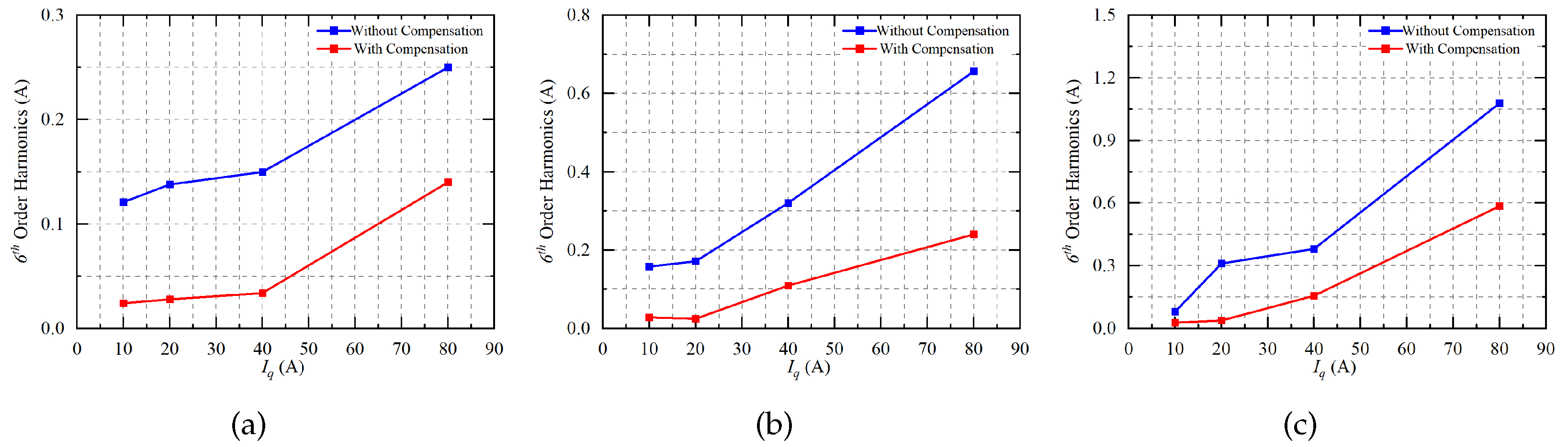
- The proposed compensation method can alleviate the 6th-order harmonic in the q-axis current, whether the modulation index is large or small. As a result, reduced torque ripples, as well as attenuated high-order noises, can be achieved, which is essential for enhancing the performance of the motor drives.
Author Contributions
Funding
Data Availability Statement
Conflicts of Interest
References
- Zhao, Y.F.; Yan, F.W.; Du, C.Q. Fast start-up control method of PMSM based on incremental photoelectric encoder. In Proceedings of the IET International Conference on Information Science and Control Engineering 2012 (ICISCE 2012), Shenzhen, China, 7–9 December 2012; pp. 1–4. [Google Scholar]
- Khanh, P.Q.; Dat, N.T.; Anh, H.P.H. Optimal Fuzzy-PI PMSM Speed Control Using Evolutionary DE Algorithm Implemented on DSP Controller. In Proceedings of the 2023 International Conference on System Science and Engineering (ICSSE), Ho Chi Minh City, Vietnam, 27–28 July 2023; pp. 206–211. [Google Scholar]
- Zhong, L.; Rahman, M.F. Analysis of direct torque control in permanent magnet synchronous motor drives. IEEE Trans. Power Electron. 1997, 12, 528–536. [Google Scholar] [CrossRef]
- Liu, H.; Li, S. Speed Control for PMSM Servo System Using Predictive Functional Control and Extended State Observer. IEEE Trans. Ind. Electron. 2012, 59, 1171–1183. [Google Scholar] [CrossRef]
- Li, S.; Liu, Z. Adaptive Speed Control for Permanent-Magnet Synchronous Motor System with Variations of Load Inertia. IEEE Trans. Ind. Electron. 2009, 56, 3050–3059. [Google Scholar]
- Khanh, P.Q.; Anh, H.P.H. Hybrid optimal fuzzy Jaya technique for advanced PMSM driving control. Electr. Eng. 2023, 105, 3629–3646. [Google Scholar] [CrossRef]
- Lei, J.; Fang, S.; Huang, D.; Wang, Y. Enhanced Deadbeat Predictive Current Control for PMSM Drives Using Iterative Sliding Mode Observer. IEEE Trans. Power Electron. 2023, 38, 13866–13876. [Google Scholar] [CrossRef]
- Seo, J.H.; Choi, C.H.; Hyun, D.S. A new simplified space-vector PWM method for three-level inverters. IEEE Trans. Power Electron. 2001, 16, 545–550. [Google Scholar]
- Casadei, D.; Profumo, F.; Serra, G.; Tani, A. FOC and DTC: Two viable schemes for induction motors torque control. IEEE Trans. Power Electron. 2002, 17, 779–787. [Google Scholar] [CrossRef]
- Singh, G.K.; Nam, K.; Lim, S.K. A simple indirect field-oriented control scheme for multiphase induction machine. IEEE Trans. Ind. Electron. 2005, 52, 1177–1184. [Google Scholar] [CrossRef]
- Rodriguez, J.; Kennel, R.M.; Espinoza, J.R.; Trincado, M.; Silva, C.A.; Rojas, C.A. High-Performance Control Strategies for Electrical Drives: An Experimental Assessment. IEEE Trans. Ind. Electron. 2012, 59, 812–820. [Google Scholar] [CrossRef]
- Xu, F.; Liu, J.; Zhang, X. Analysis of Deadtime Effects and Optimum Deadtime Control for Bidirectional Inductive Power Transfer Converters. IEEE Trans. Ind. Electron. 2023, 1–9. [Google Scholar] [CrossRef]
- Munoz, A.; Lipo, T. On-line dead-time compensation technique for open-loop PWM-VSI drives. IEEE Trans. Power Electron. 1999, 14, 683–689. [Google Scholar] [CrossRef]
- Choi, J.W.; Sul, S.K. Inverter output voltage synthesis using novel dead time compensation. IEEE Trans. Power Electron. 1996, 11, 221–227. [Google Scholar] [CrossRef]
- Tong, S.; Li, Y. Adaptive Fuzzy Output Feedback Control of MIMO Nonlinear Systems with Unknown Dead-Zone Inputs. IEEE Trans. Fuzzy Syst. 2013, 21, 134–146. [Google Scholar] [CrossRef]
- Jeong, S.G.; Park, M.H. The analysis and compensation of dead-time effects in PWM inverters. IEEE Trans. Ind. Electron. 1991, 38, 108–114. [Google Scholar] [CrossRef]
- Dolguntseva, I.; Krishna, R.; Soman, D.E.; Leijon, M. Contour-Based Dead-Time Harmonic Analysis in a Three-Level Neutral-Point-Clamped Inverter. IEEE Trans. Ind. Electron. 2015, 62, 203–210. [Google Scholar] [CrossRef]
- Yuruk, H.; Keysan, O.; Ulutas, B. Comparison of the Effects of Nonlinearities for Si MOSFET and GaN E-HEMT Based VSIs. IEEE Trans. Ind. Electron. 2021, 68, 5606–5615. [Google Scholar] [CrossRef]
- Xiang, D.; Yang, J.; Hao, Y.; Xu, G. Two-Parameter Identification Method of Deadtime Effect Voltage Error Model during Self-Commission. IEEE Trans. Power Electron. 2023, 38, 15904–15920. [Google Scholar] [CrossRef]
- Wu, M.; Zhao, R.; Tang, X. Study of Vector-Controlled Permanent Magnet Synchronous Motor at Low Speed and Light Load. Trans. China Electrotech. Soc. 2005, 07, 87–92. [Google Scholar]
- Cao, X.; Fan, L. Dead-Time Compensation for PMSM Drive Based on Neuro-Fuzzy Observer. In Proceedings of the 2008 Fourth International Conference on Natural Computation, Jinan, China, 18–20 October 2008; Volume 2, pp. 46–50. [Google Scholar]
- Lee, D.H.; Ahn, J.W. A Simple and Direct Dead-Time Effect Compensation Scheme in PWM-VSI. IEEE Trans. Ind. Appl. 2014, 50, 3017–3025. [Google Scholar] [CrossRef]
- El-Daleel, M.S.; Mahgoub, O.; Elshafei, A.L.; Mahgoub, A. Inverter dead-time and non-linearity rejection using a wide bandwidth current controller for PMSM drives with a speed sensor. In Proceedings of the 2016 Eighteenth International Middle East Power Systems Conference (MEPCON), Cairo, Egypt, 27–29 December 2016; pp. 687–692. [Google Scholar]
- Urasaki, N.; Senjyu, T.; Kinjo, T.; Funabashi, T.; Sekine, H. Dead-time compensation strategy for permanent magnet synchronous motor drive taking zero-current clamp and parasitic capacitance effects into account. In Proceedings of the 30th Annual Conference of IEEE Industrial Electronics Society, Busan, Republic of Korea, 2–6 November 2004; Volume 152, pp. 845–853. [Google Scholar]
- Urasaki, N.; Senjyu, T.; Uezato, K.; Funabashi, T. Adaptive Dead-Time Compensation Strategy for Permanent Magnet Synchronous Motor Drive. IEEE Trans. Energy Convers. 2007, 22, 271–280. [Google Scholar] [CrossRef]
- Urasaki, N.; Senjyu, T.; Uezato, K.; Funabashi, T. An adaptive dead-time compensation strategy for voltage source inverter fed motor drives. IEEE Trans. Power Electron. 2005, 20, 1150–1160. [Google Scholar] [CrossRef]
- Li, C.; Gu, Y.; Li, W.; He, X.; Dong, Z.; Chen, G.; Ma, C.; Zhang, L. Analysis and compensation of dead-time effect considering parasitic capacitance and ripple current. In Proceedings of the 2015 IEEE Applied Power Electronics Conference and Exposition (APEC), Charlotte, NC, USA, 15–19 March 2015; pp. 1501–1506. [Google Scholar]
- Zhang, Z.; Xu, L. Dead-Time Compensation of Inverters Considering Snubber and Parasitic Capacitance. IEEE Trans. Power Electron. 2014, 29, 3179–3187. [Google Scholar] [CrossRef]
- Tang, Z.; Akin, B. Suppression of Dead-Time Distortion Through Revised Repetitive Controller in PMSM Drives. IEEE Trans. Energy Convers. 2017, 32, 918–930. [Google Scholar] [CrossRef]
- Hwang, S.H.; Kim, J.M. Dead Time Compensation Method for Voltage-Fed PWM Inverter. IEEE Trans. Energy Convers. 2010, 25, 1–10. [Google Scholar] [CrossRef]
- Kim, S.Y.; Park, S.Y. Compensation of Dead-Time Effects Based on Adaptive Harmonic Filtering in the Vector-Controlled AC Motor Drives. IEEE Trans. Ind. Electron. 2007, 54, 1768–1777. [Google Scholar] [CrossRef]
- Yang, K.; Yang, M.; Lang, X.; Lang, Z.; Xu, D. An adaptive dead-time compensation method based on Predictive Current Control. In Proceedings of the 2016 IEEE 8th International Power Electronics and Motion Control Conference (IPEMC-ECCE Asia), Hefei, China, 22–26 May 2016; pp. 121–125. [Google Scholar]
- Gui, H.; Zhang, Z.; Ren, R.; Chen, R.; Niu, J.; Tolbert, L.M.; Wang, F.; Blalock, B.J.; Costinett, D.J.; Choi, B.B. SiC MOSFET Versus Si Super Junction MOSFET-Switching Loss Comparison in Different Switching Cell Configurations. In Proceedings of the 2018 IEEE Energy Conversion Congress and Exposition (ECCE), Portland, OR, USA, 23–27 September 2018; pp. 6146–6151. [Google Scholar]
- Wang, G.; Wang, F.; Magai, G.; Lei, Y.; Huang, A.; Das, M. Performance comparison of 1200 V 100 A SiC MOSFET and 1200 V 100 A silicon IGBT. In Proceedings of the 2013 IEEE Energy Conversion Congress and Exposition (ECCE), Denver, CO, USA, 15–19 September 2013; pp. 3230–3234. [Google Scholar]
- Xie, Y.; Chen, C.; Yan, Y.; Huang, Z.; Kang, Y. Investigation on Ultra-low Turn-off Losses Phenomenon for SiC MOSFETs with Improved Switching Model. IEEE Trans. Power Electron. 2021, 36, 9382–9397. [Google Scholar] [CrossRef]
- Hava, A.; Kerkman, R.; Lipo, T. A high-performance generalized discontinuous PWM algorithm. IEEE Trans. Ind. Appl. 1998, 34, 1059–1071. [Google Scholar] [CrossRef]


| − | ↑ | ↑ | ↑ | ↑ |
| Normal Turn-Off | QZCS Turn-Off | ||||||
|---|---|---|---|---|---|---|---|
| ↓ | ↓ | ↓ | ↓ | ↑ | ↓ | ↓ | ↓ |
| (A) | (ns) | (ns) | (ns) | (ns) | (ns) | (ns) | |
|---|---|---|---|---|---|---|---|
| 0.3 | 71 | 44.4 | 122.8 | 668.4 | 115.4 | 791.2 | |
| 0.5 | 74.8 | 43.2 | 124 | 425.6 | 118 | 549.6 | |
| 2 | 76 | 45.2 | 111.6 | 102.8 | 121.2 | 214.4 | |
| 5 | 71.6 | 48.8 | 105.6 | 53.2 | 120.4 | 158.8 | |
| 10 | 68.5 | 40.8 | 103.2 | 48 | 109.3 | 151.2 | |
| 20 | 70.2 | 51.2 | 99.8 | 46.4 | 121.4 | 146.2 | |
| 40 | 66 | 57.2 | 96.4 | 44 | 123.2 | 140.4 | |
| 80 | 68.4 | 91.2 | 83.6 | 42.4 | 159.6 | 126 | |
| 0.3 | 78.8 | 36.8 | 124 | 638.8 | 115.6 | 791.2 | |
| 0.5 | 74.8 | 36.4 | 128.8 | 449.2 | 113.6 | 549.6 | |
| 2 | 76 | 38 | 114.8 | 101.6 | 113.2 | 214.4 | |
| 5 | 71.6 | 41.2 | 114.4 | 49.2 | 120.4 | 158.8 | |
| 10 | 70.4 | 41.2 | 107.6 | 44.4 | 111.6 | 152 | |
| 20 | 69.2 | 46.4 | 101.6 | 42 | 115.6 | 143.6 | |
| 40 | 68.8 | 64.4 | 95.2 | 40 | 133.2 | 135.2 | |
| 80 | 70.8 | 98 | 90.8 | 39.6 | 168.8 | 130.4 |
| Parameters | Value | Parameters | Value |
|---|---|---|---|
| Stator d-axis inductance () | 70 H | Number of pole-pairs (p) | 4 |
| Stator q-axis inductance () | 70 H | Rated current () | 80 A |
| PM fux linkage () | 0.006547 Wb | DC bus voltage () | 12 V |
| Stator resistance () | 11 m |
Disclaimer/Publisher’s Note: The statements, opinions and data contained in all publications are solely those of the individual author(s) and contributor(s) and not of MDPI and/or the editor(s). MDPI and/or the editor(s) disclaim responsibility for any injury to people or property resulting from any ideas, methods, instructions or products referred to in the content. |
© 2023 by the authors. Licensee MDPI, Basel, Switzerland. This article is an open access article distributed under the terms and conditions of the Creative Commons Attribution (CC BY) license (https://creativecommons.org/licenses/by/4.0/).
Share and Cite
Liu, X.; Li, H.; Wu, Y.; Wang, L.; Yin, S. Dynamic Dead-Time Compensation Method Based on Switching Characteristics of the MOSFET for PMSM Drive System. Electronics 2023, 12, 4855. https://doi.org/10.3390/electronics12234855
Liu X, Li H, Wu Y, Wang L, Yin S. Dynamic Dead-Time Compensation Method Based on Switching Characteristics of the MOSFET for PMSM Drive System. Electronics. 2023; 12(23):4855. https://doi.org/10.3390/electronics12234855
Chicago/Turabian StyleLiu, Xi, Hui Li, Yingzhe Wu, Lisheng Wang, and Shan Yin. 2023. "Dynamic Dead-Time Compensation Method Based on Switching Characteristics of the MOSFET for PMSM Drive System" Electronics 12, no. 23: 4855. https://doi.org/10.3390/electronics12234855
APA StyleLiu, X., Li, H., Wu, Y., Wang, L., & Yin, S. (2023). Dynamic Dead-Time Compensation Method Based on Switching Characteristics of the MOSFET for PMSM Drive System. Electronics, 12(23), 4855. https://doi.org/10.3390/electronics12234855