Article

Efficient Hardware Implementation of Elliptic-Curve Diffie–Hellman Ephemeral on Curve25519

1
Department of Electronics, Faculty of Electrical-Electronics, Ho Chi Minh City University of Technology (HCMUT), 268 Ly Thuong Kiet Street, District 10, Ho Chi Minh City 700000, Vietnam
2
Vietnam National University Ho Chi Minh City (VNU-HCM), Linh Trung Ward, Thu Duc District, Ho Chi Minh City 700000, Vietnam
*
Author to whom correspondence should be addressed.
These authors contributed equally to this work.
Electronics 2023, 12(21), 4480; https://doi.org/10.3390/electronics12214480
Submission received: 15 September 2023 / Revised: 26 October 2023 / Accepted: 26 October 2023 / Published: 31 October 2023
(This article belongs to the Section Circuit and Signal Processing)

Abstract

:
Hardware architecture optimized for implementing the elliptic-curve Diffie–Hellman ephemeral (ECDHE) on 256-bit Montgomery elliptic curves presents unique challenges, particularly for resource-constrained IoT and mobile devices. This work aims to provide an efficient hardware implementation of ECDHE on Curve25519, including a dedicated finite state machine (FSM) designed to handle point multiplication and ECDHE operations, utilizing constant-time algorithms and a unified memory block for resource management. Additionally, we introduce an optimized modular computation unit that covers modular addition, subtraction, multiplication, and inversion. Our proposed hardware architecture enhances the efficiency of ECDHE operations while maintaining low resource utilization, considerably reduced latency, and low power consumption. Synthesized on the Xilinx Artix-7 platform, our design boasts 64,000 Slices and a clock speed of 102 MHz, and it computes an ECDHE scalar multiplication operation in 1.1 ms, consuming 117 mW. The proposed hardware design can be applied to various platforms, including mobile devices and IoT systems.

1. Introduction

The Internet is much more encrypted now than it was in the past. Information is much more secure with the widespread application and usage of Internet security protocols, such as elliptic curve cryptography (ECC) in Transport Layer Security (TLS) [1,2]. The standard requires many devices, including personal computers, smartphones, and Internet of Things (IoT) devices, to compute cryptography encryption and decryption whenever they communicate over the World Wide Web.
While practical ECC computations are crucial in safeguarding user data privacy on mobile and IoT devices, the primary bottlenecks are the limited processing power and energy resources of these devices. Hardware implementation is designed to increase computational speed and reduce energy consumption through paralleling techniques used on low-power microcontrollers or mobile phones.
Many methods for calculating and processing ECC on hardware differ in performance, area, occupied memory, power consumption, and security level. We focus on putting our design onto a field-programmable gate array (FPGA). Research by Izu et al. [3] shows a method that applies simple algorithms and utilizes the FPGA structure to achieve high efficiency, which is a trade-off with the area. The above study also builds on the original work of Aoki et al. [4]. One of the initial adoptions of digital signal processors (DSPs) for modular operation is from [5]. While using a DSP has the advantage of fast computational speed, it requires the DSP resource to be available and consume more power. To enhance a modular addition, Rogawski et al. suggested using fast carry chain adders [6] based on a parallel prefix network [7]. The result is better speed in modular adding and subtracting operations, with a trade-off with latency of pipeline stages. For modular multiplication, the choice is between a high-radix multiplier [8] or high-density karatsuba with NLP multiplication [9]. A high radix level increases the complexity of the design, and it is better to compensate for the low radix level with better hardware adders. Redundant binary representation is another notable method for modular multipliers [10]. P. Kocher et al. pointed out that the vulnerability to power analysis attacks is notable in the hardware design for cryptography processing in FPGAs [11]. Fischer et al. also gave an example structure against energy analysis [12].
In the case of Curve25519, Sasdrich et al. presented the first Curve25519 hardware design [13]. Kopperman et al. presented two Curve25519 hardware implementations that could process ECDHE scalar multiplication under 100 μ s [14,15]. Interleaved modular multipliers were used in research [16] to reduce power consumption. Niasar et al. [17] presented three designs with low resource requirements, area–time efficiency, and high performance. Research [18] showed a hardware–software hybrid design for resource-constrained devices. Research [19] showed scalable point multiplication for Curve25519. Kudithi et al. [20] implemented their design with a radix-2 multiplier, using mixed Jacobian coordinates on different FPGA platforms and application-specific integrated circuits (ASIC). With different parameters, Kieu et al. [21] supported multiple curves on their FPGA and ASIC designs.
Our research is to create a hardware design that handles cryptography operation for the TLS curve Curve25519 [22]. The ECC operation includes elliptic-curve Diffie–Hellman ephemeral (ECDHE) key generation and computation.
The main contribution of this paper includes creating a hardware design structure that can do the following:
  • Generate the public key for ECDHE and compute the shared key according to IEEE P1363 [23] with support for the TLS 256-bit elliptic curve Curve25519 [2].
  • Employ a fast elliptic computation unit optimized for modular addition, subtraction, multiplication, and inversion.
  • Comprise a specialized finite state machine (FSM) that executes point multiplication and ECDHE operations, utilizing a constant-time algorithm and relying on a single consolidated memory block to optimize resource utilization.
The remaining sections of this paper are structured as follows. Section 2 provides an overview of the mathematical backgrounds and parameters of Curve25519. Section 3 is the proposed hardware design for implementing Curve25519 elliptic-curve Diffie–Hellman ephemeral (ECDHE) processes. Our findings and results are elaborated upon in Section 4. Section 5 discusses our design, including comparisons with relevant references. Section 6 concludes and summarizes this paper.

2. Backgrounds

2.1. Elliptic Curve Cryptography Mathematics

ECC is based on a finite field in the form of an integer mod p, where p is prime. A field F is a set of elements with addition and multiplication operators. For every element a in field F, except 0, there exists an element a 1 F so that a a 1 = 1 .
In a finite field of order p (prime field), for a prime number p, a finite field of degree p, G F ( p ) , is defined as the set Z p = 0 , 1 , , p 1 , with the algebraic operations modulo p. Each element in Z p (except 0) has a modular inverse (i.e., there exists z, w Z p such that wz = 1 mod p or z = w 1 mod ( p ) ).

2.2. Curve25519 Parameters

The curve presented in this paper is Curve25519 (Montgomery curve). Table 1 presents the parameters and corresponding values of Curve25519 from standards [24,25,26]. These are the values used in the hardware design proposed in the paper. The curve is defined in a prime field with the prime p close to a power of 2 to optimize the efficiency of modulo computations.

2.3. Computation on Montgomery Curve

A Montgomery curve on the field F p is in the following form:
B y 2 = x 3 + A x 2 + x ( A , B F p , B 0 , A 2 4 )
On the projective coordinate system, with x = X Z and y = Y Z , the form is presented in the function below. Notice that Y is no longer needed. P x : y is now P ( X : Z ) with Z 0 . There are two special points O = 0 : 1 : 0 and T = ( 0 : 0 : 1 ) that are converted to O = 1 : 0 and T = ( 0 : 0 ) .
This form allows us to use the Montgomery powering ladder algorithm to compute scalar multiplication on the Montgomery curve. A modified version of this algorithm is preferred because of the side-channel attack prevention [27].

2.4. Elliptic-Curve Diffie–Hellman Ephemeral (ECDHE)

ECDHE is the method used during the key exchange between the server and the client so that the result is a pre-master secret known to both parties. During the handshake, after the server and client have agreed on which cipher suite and curve to use, both of them know the parameter domain, including the following values:
  • p: prime number p defined for the field F p
  • a: parameters of the curve equation
  • S ( u , v ) : coordinates of base point (generator)
  • n: order of S, defined as the smallest integer for which n S = 0
  • h: the cofactor
The pre-master secret agreement process is as follows:
  • The server chooses a random number k < ( 0 < k < n ) . Then, the server calculates k S and sends it to the client.
  • The client chooses a random number k   ( 0 < k < n ) . The client calculates k S and sends it to the server.
  • Server and client, after obtaining the ephemeral data k or k of the other end, can calculate the pre-master secret P = k k S = k k S

3. Hardware Design

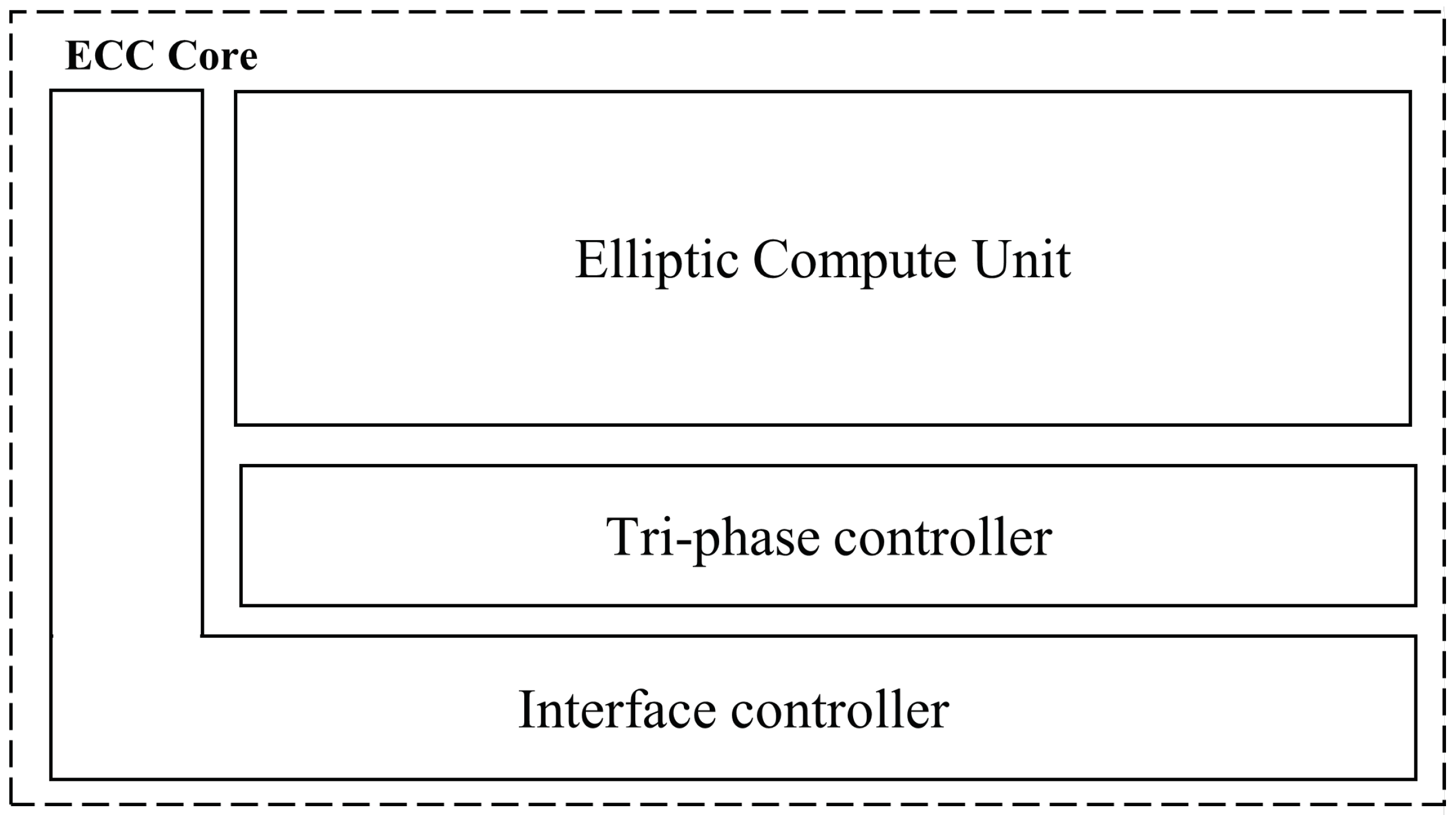
The ECC Core is the proposed hardware structure for implementing elliptic curve cryptography over Curve25519. The ECC Core features a data input bus and start signal along with a mode input for choosing between modes of operation. The calculation status is updated to the output, and the result follows.
The design method is implemented as intuitive, easy-to-modify hardware modules that can work individually with their tasks. The ECU handles modular addition, subtraction, multiplication, and inversion. The Figure 1 presents the structure of the ECC Core. It includes an interface controller, a tri-phase controller, and an ECU.
The interface controller handles data output and input, mode selection, and testing purposes. The tri-phase controller (TPC) is the finite state machine (FSM) for scalar multiplication, random number generation, memory interface, etc., to serve the ECDHE key generation and computation process. The ECU processes modular arithmetic tasks given by the TPC.

3.1. Interface Controller

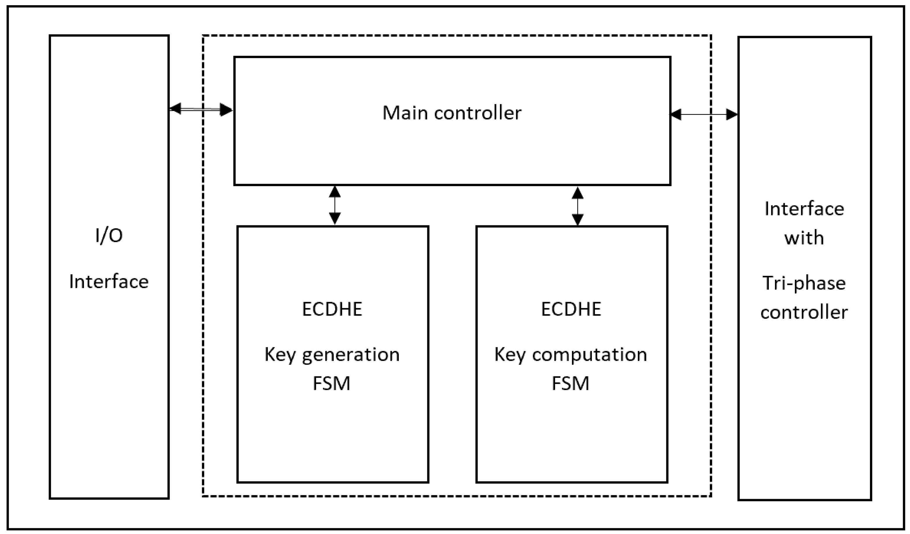
The interface controller connects the system’s primary input and output interfaces to the TPC. It also does random number generation and error checking for invalid values during computation. Figure 2 shows the general structure of the interface controller with dedicated FSMs for receiving the input and processing ECDHE key generation and computation. The input received is 512-bit in parallel for ease of computation. We synthesized our design with another serial-to-parallel interface to eliminate the pin issue. The I/O interface has 32-bit input and output controlled with ready, acknowledge, and a busy flag to receive or output data from the memory in 32-bit chunks. We designed the FSMs so that the state transitions depend only on the current state and mode input, minimizing complex logic. This simplistic FSM architecture provides low-latency performance while minimizing the attack surfaces side-channel leaking and improving security [28].
For ECDHE key generation and computation, the first 256-bit of the input is u, and the latest 256-bit is k. 
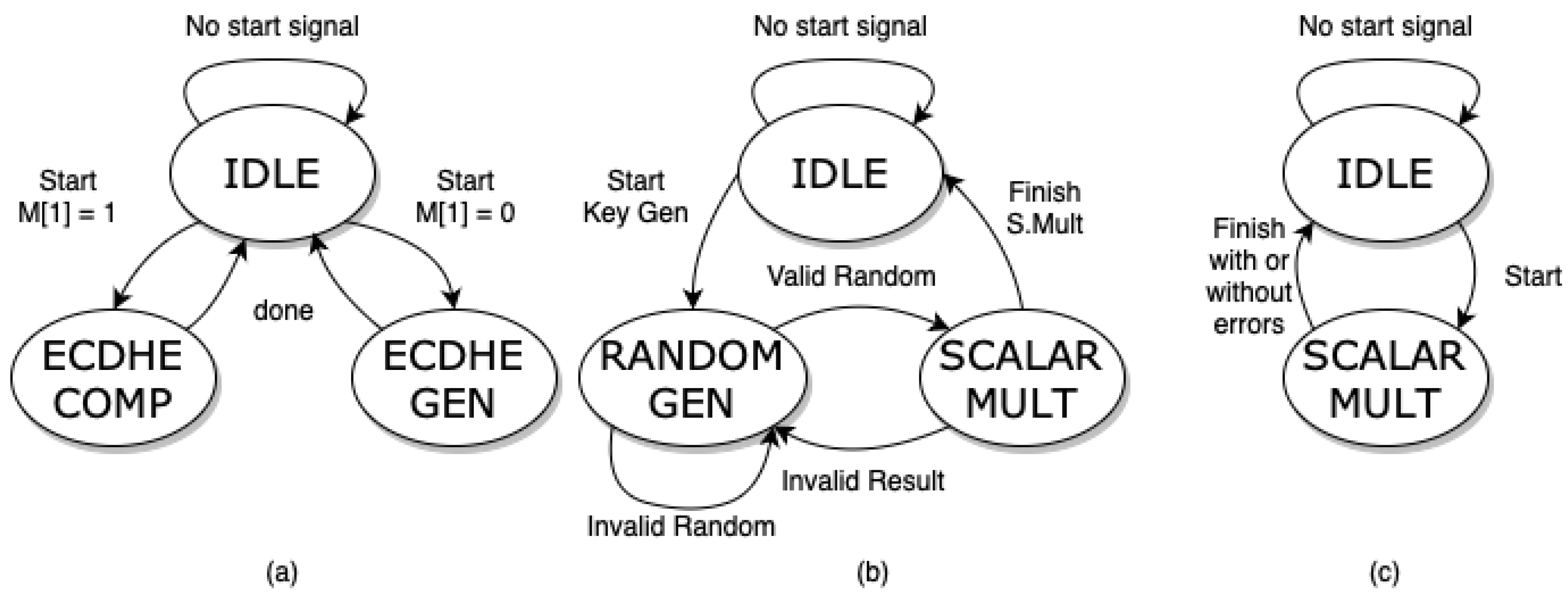
Figure 3 shows the three FSMs. Figure 3a is the interface controller FSM that interacts with the ECDHE generation FSM (Figure 3b) and ECDHE computation FSM (Figure 3c).
The interface controller FSM (a) waits for the start signal and reads the mode input M[1] from the I/O interface to choose between the ECDHE key generation operation or ECDHE key computation. The ECDHE key generation FSM (b) starts with the random generation of k. If k is non-zero, we start the scalar multiplication operation with P from the curve parameter Table 1. If the result returns an invalid point (point at infinity or zero), the random generation process starts again to obtain another random k for calculation. The ECDHE computation FSM (c) instructs the tri-phase controller to obtain the data from memory and start the scalar multiplication process.
The ECDHE generation procedure starts with choosing a random k (and repeating if k is not valid), computing scalar multiplication, and checking for validation (Q is not point zero) according to Section 2.4. The ECDHE computation procedure receives data from the input and computes the scalar multiplication. Then, it checks for validation (P is not point zero).

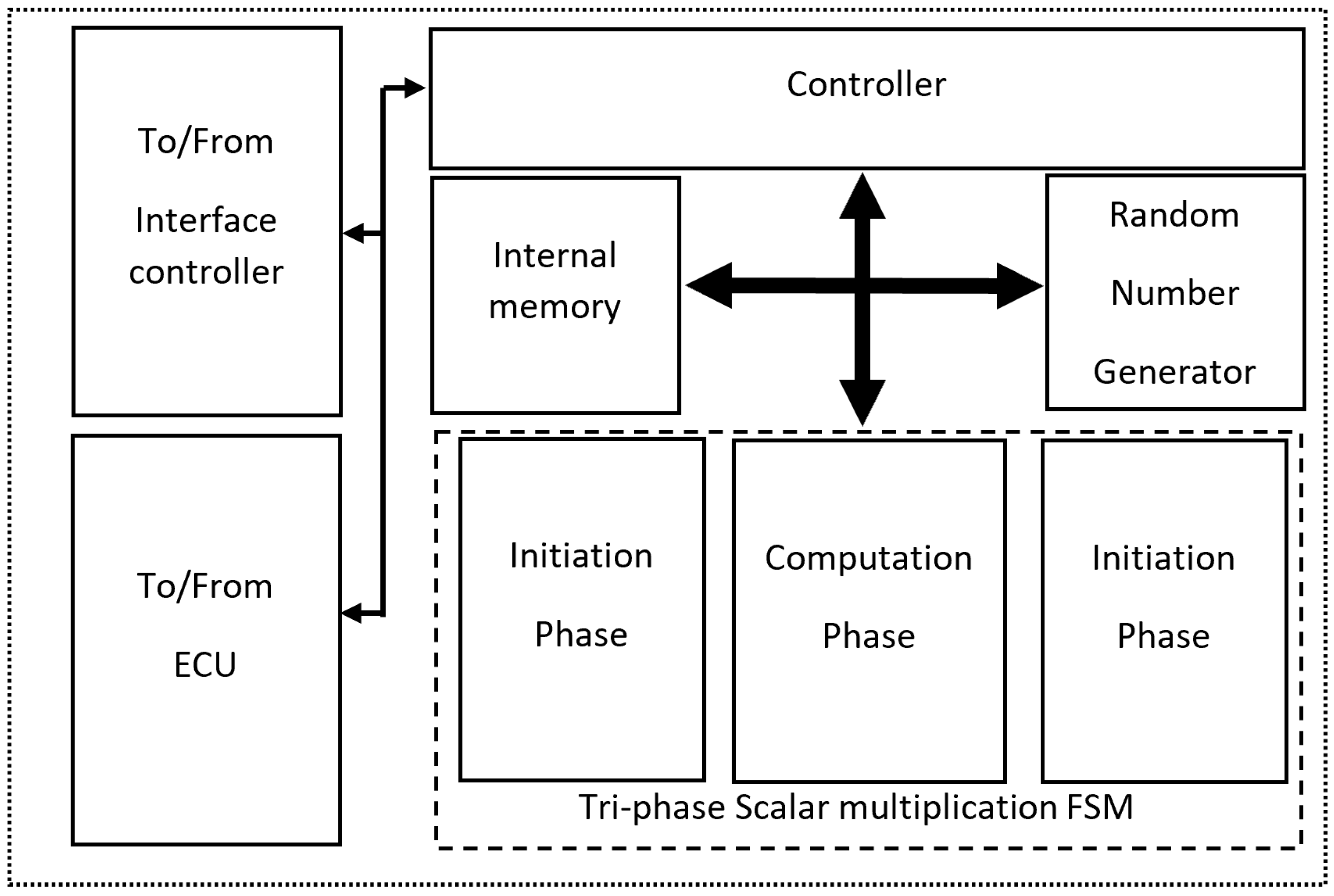
3.2. Tri-Phase Controller

The tri-phase controller interacts with the interface controller and the ECU and controls its internal memory block. We use a BRAM as the internal memory block where values are generated between each operation in the memory. The memory size used is 32 × 256-bit, enough for operations on 256-bit operands of ECDHE key generation and computation. Figure 4 presents the structural diagram of the tri-phase controller.

3.2.1. Internal Memory Access

We use 32 × 256-bit random access memory with a synchronous read-and-write clock. We use 23 addresses as storage for global variables and 9 as temporary variables. The number is to accommodate the modified scalar multiplication for Montgomery curves. Table 2 shows how we named each address. The names correspond to the variables in Algorithm 1.
Algorithm 1 Modified scalar multiplication for Montgomery curves.
1:
x 1 = u , x 2 = 1 , z 2 = 0 , x 3 = u , z 3 = 1 , s w a p = 0 , a 24 = 121,665
2:
for ( t = b i t s 1 down to 0) do
3:
      s w a p = s w a p k [ t ]
4:
      ( x 2 , x 3 ) = S W A P ( s w a p , x 2 , x 3 )
5:
      ( z 2 , z 3 ) = S W A P ( s w a p , z 2 , z 3 )
6:
      s w a p = k [ t ]
7:
      A = x 2 + z 2
8:
      A A = A 2
9:
      B = x 2 z 2
10:
    B B = B 2
11:
    E = A A B B
12:
    C = x 3 + z 3
13:
    D = x 3 z 3
14:
    D A = D A
15:
    C B = C B
16:
    x 3 = ( D A + C B ) 2
17:
    z 3 = x 1 ( D A C B ) 2
18:
    x 2 = A A B B
19:
    z 2 = E ( A A + a 24 E )
20:
end for
21:
( x 2 , x 3 ) = S W A P ( 0 , x 2 , x 3 )
22:
( z 2 , z 3 ) = S W A P ( 0 , z 2 , z 3 )
23:
return  x 2 ( M O N T I N V ( z 2 ) )

3.2.2. Tri-Phase Scalar Multiplication for Montgomery Curves

The algorithm used in the design to perform scalar multiplication for Montgomery elliptic curves (here, we use curve X25519) is S.Turner’s algorithm [24,27]. This algorithm ensures the constant-time characteristic for all input values.
Because the original algorithm is written in Python for software, we made some changes to the algorithm to make it suitable for hardware. The modified algorithm is shown in Algorithm 1. The constant a 24 is ( 486,662 2 ) / 4 = 121,665 for curve25519/X25519. Specifically, the following process is performed:
  • Remove the k shift and switch to indexing.
  • Drop the swap value on the last two swaps because the last 3 bits of k are always zero after correctly decoding in RFC 7748 [24].
  • Remove the last exponent. Montgomery exponential can be performed on hardware, but it takes too much time; instead, Montgomery inverse gives the same result, which is proved below:
    We can quickly prove that the Montgomery exponential step is the Montgomery inverse.
    Given t = a 1 m o d p and t = a p 2 m o d p
    a t m o d p = 1 m o d p
    a a p 2 m o d p = 1 m o d p
    a p 1 m o d p = 1 m o d p
    This is Fermat’s little theorem [29].
Montgomery scalar multiplier is divided into three parts. The structural diagram for the multiplier is presented in the tri-phase scalar multiplication FSM in Figure 4.
  • Initialization phase (init)
    -
    Initialize values in the memory block.
    -
    Decode the input scalar value in the form 2 254 + 8 r a n d o m ( 0 , 2 255 1 ) and convert it from Little-Endian to an integer.
    -
    Decode the input point coordinate value, convert little-endian to an integer, and give the mask to bit 256.
  • Calculation phase (comp)
    -
    Perform the loop of swapping, multiplying, and adding points 255 times.
    -
    Interact with ECU’s internal memory from 45-state FSM.
  • Final phase
    -
    Perform the final calculation with one Montgomery inverse and one Montgomery multiplication.
    -
    Normalize and save the result in the internal memory.
Appendix A shows the operations we execute in each step of the finite state machine for each phase in the tri-phase controller. The operation accesses the corresponding address in the internal memory to store or load necessary values for computation.

3.3. Random Number Generator

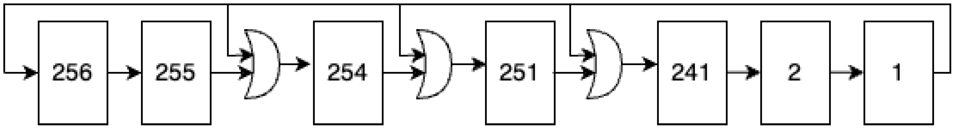
We utilize a pseudo-random number generator (PRNG) to generate random numbers. Generally, we adopt a linear feedback shift register design, as outlined in [30], with adjustments to accommodate a 256-bit format. Feedback is incorporated at specific positions: 256, 254, 251, and 246. PRNGs are straightforward and primarily employed for simulation and testing. The structure of the Galois 256-bit LFSR is visually represented in Figure 5.

3.4. Elliptic Compute Unit

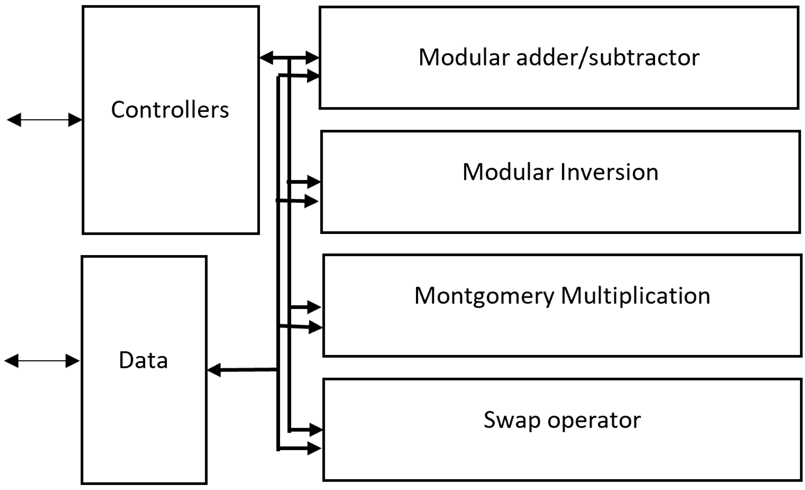
The elliptic compute unit (ECU) receives data and control signals from the tri-phase controller. It consists of four modules for four operations: modular addition, Montgomery multiplication, Montgomery inversion, and swap operator.
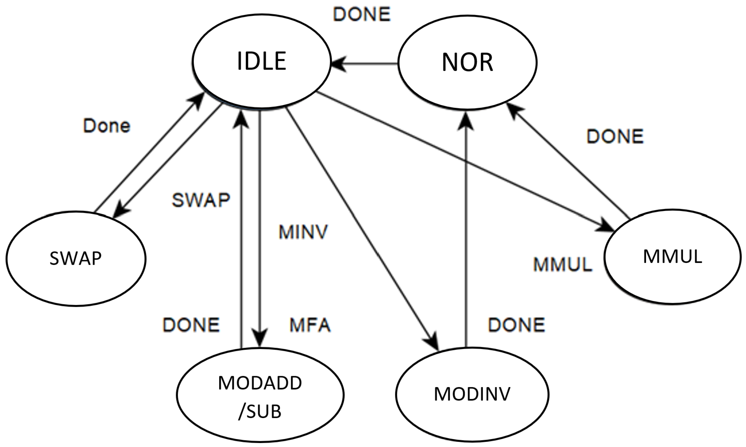
Figure 6 shows the structural diagram of the ECU, and Figure 7 presents the controller state machine of the ECU. For modular addition, subtraction, and swap state, the state machine starts the corresponding operation based on the mode selection signal and returns when the module finishes. A normalized (NOR) state is needed for modular inverse and multiplication before returning the result. The normalized state removes the excess R 2 from Montgomery multiplication and inversion. Because the ECU affects the critical path of the design heavily, we try to optimize our design on each operation unit of the ECU carefully. Every operation of the ECU is for 256-bit operands and uses a constant-time algorithm to prevent side-channel attacks.

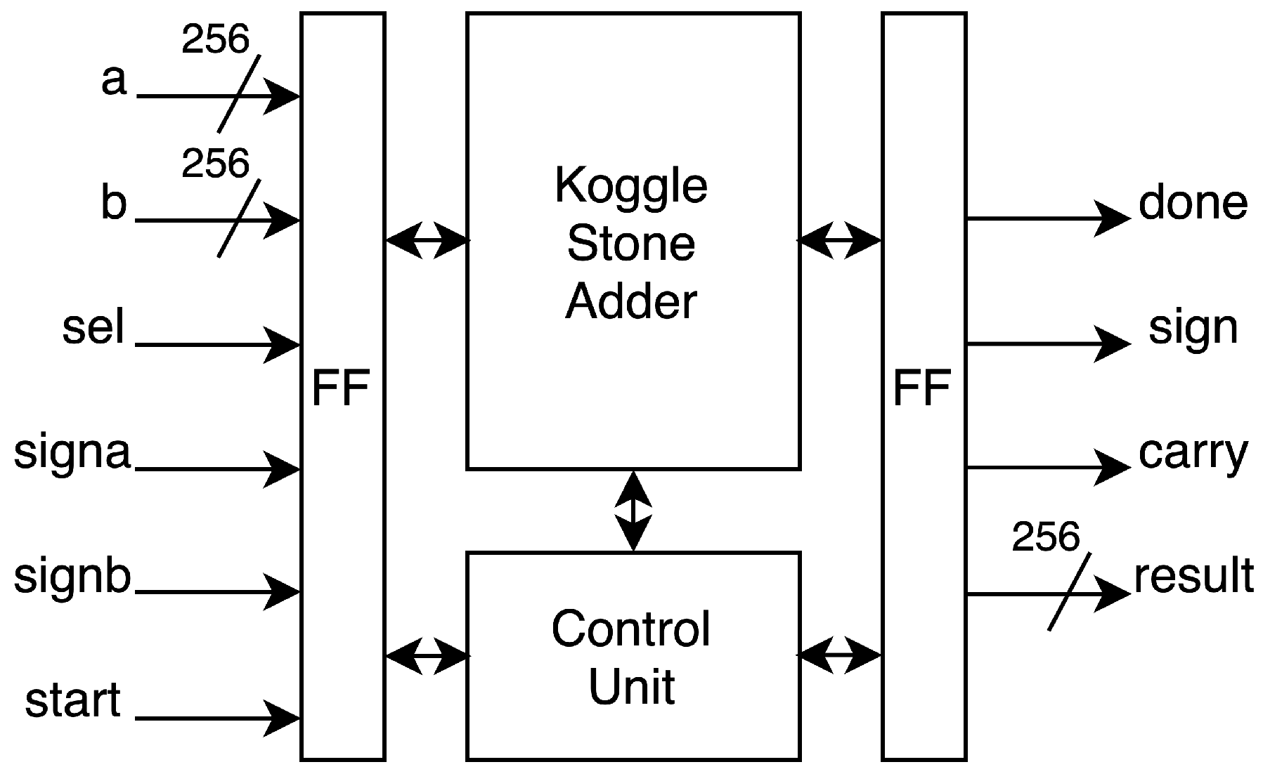
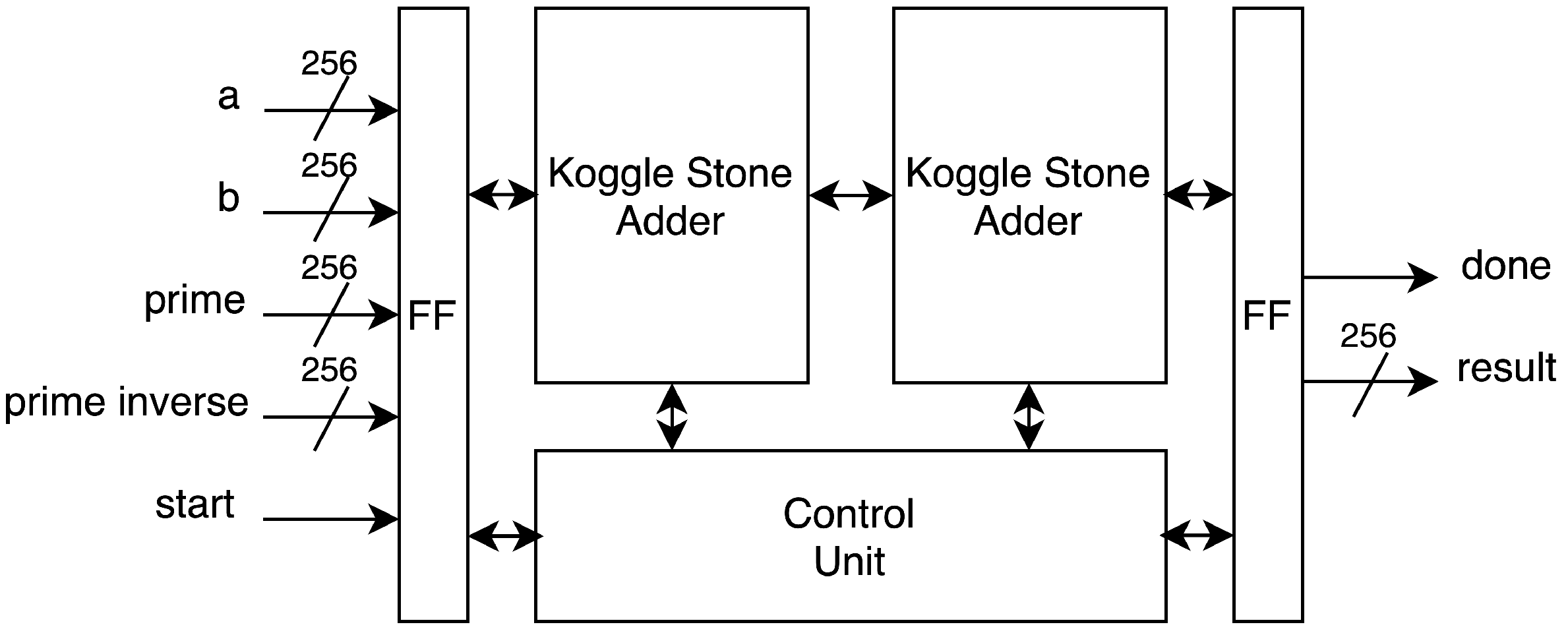
3.5. Modular Adder and Subtractor

To optimize timing for the 256-bit modular adder and subtractor, we use a Kogge–Stone adder (KSA) structure. We designed the dual-purpose modular addition and subtraction unit based on the high-radix parallel prefix network modular adder/subtractor proposed by Rogawski et al. [6]. This Koggle–Stone parallel prefix network adder/subtractor (KSA) is appropriate for optimizing operating frequency and pipeline.
The adder receives 256-bit input a and b with two MSBs processed by the controller. The low 256-bit section is the input for KSA. The controller also processes the s i g n a , s i g n b , c 1 and determines the result’s s i g n o and c o . Signal s e l selects the mode between subtraction and addition. The design has 2 clock latencies. Figure 8 provides the dual-purpose structure packed with a micro finite state machine.

3.6. Montgomery Multiplication

For modular multiplication, we utilize radix-2 Montgomery modular multiplication, as proposed by Xiao et al. [8], but modified with KSAs instead of 256-bit regular adders for high performance. Algorithm 2 shows the Montgomery modular multiplication used in the proposed design.
The hardware design for the Montgomery multiplication architecture uses the referenced algorithm with u k = 1 , u = k = 1 , which uses the mux and carry load adder and the shift register to compute the values of S through each loop. S i j computation uses 16-bit adders. R = 2 256 is a constant. It has a 256-bit input port for the Multiplicand and Multiplier a and b and the prime and pre-calculated inverse prime number. The start signal starts the operation. It completes the multiplication after 256 loops and outputs the 256-bit result and a done signal. Figure 9 shows the structural diagram.
Algorithm 2 Montgomery modular multiplication
1:
Input:  A = i = 0 i = k 1 a i 2 i , B = i = 0 i = k 1 b i 2 i , M = i = 0 i = k 1 m i 2 i , M = i n v e r s e ( M , 2 k )
2:
Output:  A B R 1 m o d M w i t h R = 2 k
3:
S = 0
4:
for ( i = 0 to n 1 ) do
5:
    S = S + b [ i ] A
6:
    q i = ( ( S m o d 2 ) M ) m o d 2 ;
7:
    S = ( S + q i N ) / 2 ;
8:
end for
9:
return  S

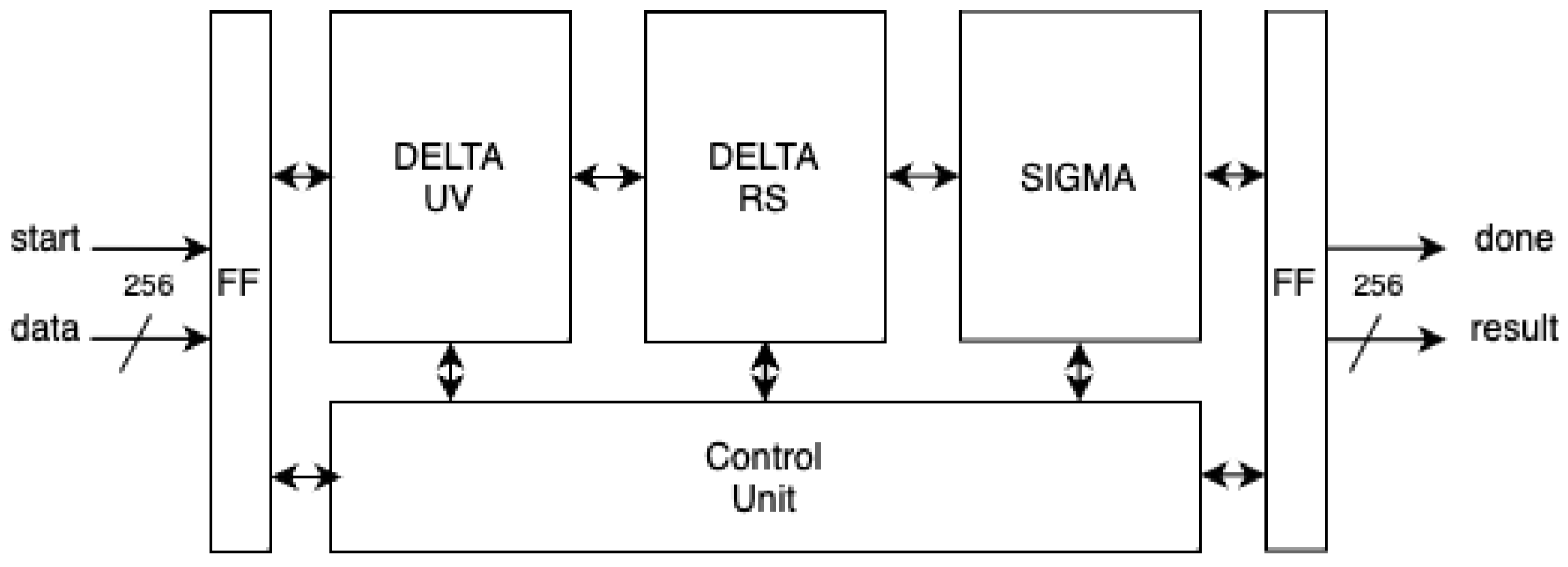
3.7. Montgomery Inversion

We design the modular inversion block based on the constant-time binary extended Euclidean algorithm proposed by Savacs [31], with modifications including Koggle–Stone adders and optimized control logic. It consists of three consecutive Koggle–Stone adder blocks (DELTA_UV, DELTA_RS, and SIGMA) performing arithmetic operations. An INV_CONTROL finite state machine controls the sequencing and operations of the DELTA_UV, DELTA_RS, and SIGMA blocks.
The algorithm computes the modular inversion result within 512 iterations, with the calculation time depending on the length of our prime value.
Figure 10 shows the structural diagram of the Montgomery inversion unit. It uses a 256-bit data input. The start signal starts the unit and resets the count from the controller to 512 loops, with u = v = r = s = 0 . We check for stage jumping between the second and eighth computation steps at each iteration. At each computationstep, delta_uv, delta_rs, and sigma are calculated sequentially. After one iteration, the value is stored and looped back until the counter reaches 0. The output is a 256-bit result and done signal.

4. Results

We used Python on Google Colab with RFC 7748 [24] and High-Assurance Cryptographic Library (HACL) [32] to build the testing environment for our design. Testing was performed with Known Answer Test (KAT) from the mentioned standards. The design was tested in the simulation environment. The simulation results show that it ran correctly for the cases outlined in the KAT of the standard ECDHE with Curve25519 from [24].
We synthesized our design on Vivado and implemented it on Xilinx Artix-7. Our design achieved a speed of 102 MHz, computing ECDHE key generation and computation in 110 thousand clock cycles. The resource utilization report shows 6409 Slice usage, zero digital signal processors (DSPs), and four block random access memories (BRAMs). Additional information regarding the resource utilization of key internal modules is provided in Table 3. Xilinx Power Estimator estimated the design power consumption at 117 m W . After 1.1 m s , the design finished the scalar multiplication operation. The value was calculated from the number of cycles it took to complete the operation times the speed of the design.

5. Discussion

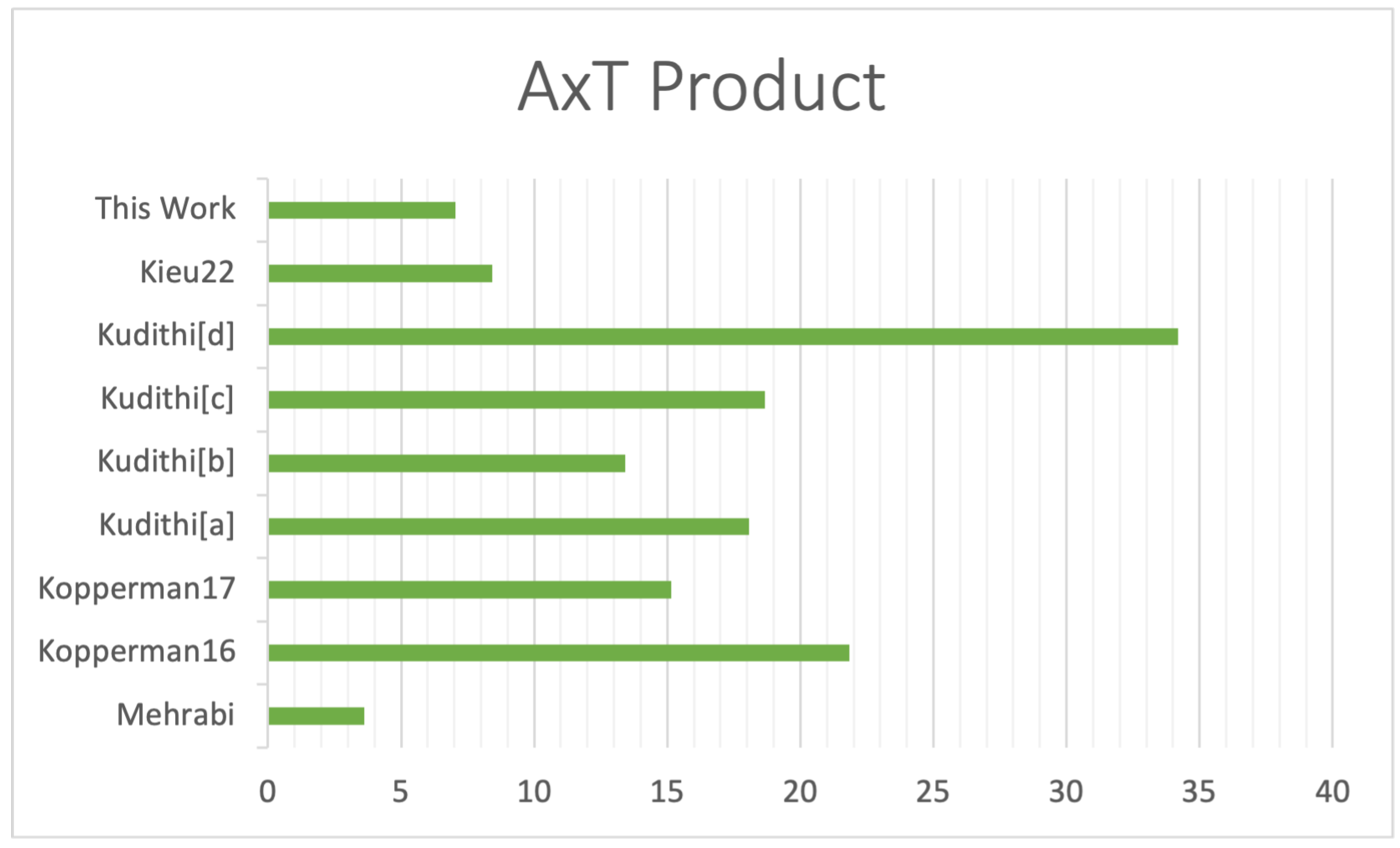
To comprehensively evaluate the efficiency of our proposed hardware architecture designed for elliptic-curve Diffie–Hellman ephemeral (ECDHE) operations on the 256-bit Montgomery Curve25519, we present a comparative analysis to relevant prior works, as summarized in Table 4. The table shows resource utilization (in Slice(s), DSP(s), BRAM(s), latency, and power consumption. To better compare to the previous result, we use a figure of merit called A × T , or area × time, where the area is in kSlices and time is the latency in m s , as shown in Equation (2), which is normalized to our proposed design.
A × T = A r e a ( k S l i c e ) T i m e ( L a t e n c y i n m s )
Our architecture has advantages in terms of resource utilization and power efficiency. With a reduced utilization of 6414 slices and four Block RAMs (BRAM), we achieved a clock frequency of 102 MHz. The latency of 1100 μ s is competitive among the listed works, even though it may be slightly higher than some implementations. The problem with using only BRAM to store data and temporary values is that it increases the latency with each ECU read-and-write operation.
Figure 11 shows the A × T products of our work and other implementations. Mehrabi et al. [16] presented a multiple multipliers implementation that commanded a higher allocation of resources and higher power usage compared to our design. However, their design did not use any BRAM, achieving a better latency and a higher A × T product than ours. However, in terms of power consumption, our design consumes only half of the power estimation. Our work’s A × T product is better than the other designs. Koppermann et al. [14,15] provided high-performance implementation with heavy DSP usage to improve their latency compared to our design, so their area factor is higher when comparing A × T values. Different implementations of [20] use the radix-2 multiplier for modular operation, achieving a good area utilization result but slower latency than ours. The design in [21] is the smallest hardware implementation in terms of area that supports Curve25519; however, they used the multiple carry saves adder to perform arithmetic operations, so their design speed was considerably slow.
While a higher clock frequency was employed in some prior works to achieve lower latencies, our approach strives for a balance between performance and energy consumption. Our architecture demonstrates efficient resource usage, making it well-suited for scenarios that prioritize secure communication and cryptographic key exchange without sacrificing substantial power resources. Our design proves to be better suited when considering lightweight FPGA and ASIC configurations devoid of DSP blocks.
The security of IoT devices is an important consideration when implementing system designs. As Di Matteo et al. [33] and Zulberti et al. [34] discussed, side-channel attacks, such as simple power analysis (SPA) and differential power analysis (DPA), on cryptographic hardware pose a significant threat. While side-channel attack countermeasures are crucial for comprehensive IoT security, an in-depth examination is beyond the scope of this paper. Our implementation focuses instead on core functionality and performance, with security considerations noted as crucial future work.

6. Conclusions

This paper introduces an efficient hardware architecture for the execution of elliptic-curve Diffie–Hellman ephemeral (ECDHE) on the 256-bit Montgomery elliptic curves, Curve25519. We introduce optimized FSMs and a structured approach to modular computation units in the design to enhance performance and resource utilization. Compared to related works, our design offers a compelling solution that balances computational power proficiency and optimized resource allocation. In future research, the latency of our design can be further improved by reducing the finite state machine overhead, implementing a register-based approach, and accessing RAM only when necessary. This approach has the potential to significantly reduce the existing latency, making our design more competitive compared to other reference implementations.

Author Contributions

Conceptualization, H.N.; methodology, H.N.; software, H.N.; validation, T.H.; formal analysis, T.H.; investigation, L.T.; resources, L.T.; data curation, H.N.; writing—original draft preparation, H.N.; writing—review and editing, T.H.; visualization, T.H.; supervision, L.T.; project administration, L.T. All authors have read and agreed to the published version of the manuscript.

Funding

This research is funded by VNU-HCM under grant number DS2022-20-05.

Institutional Review Board Statement

Not applicable.

Informed Consent Statement

Not applicable.

Data Availability Statement

Research data is available at https://github.com/hakatu/ephemeral-ecc (accessed on 1 September 2023).

Acknowledgments

This research is funded by VNU-HCM under grant number DS2022-20-05. We would like to thank Ho Chi Minh City University of Technology (HCMUT), VNU-HCM, for the support of time and facilities for this study.

Conflicts of Interest

The authors declare no conflict of interest. The funders had no role in the design of the study; in the collection, analyses, or interpretation of data; in the writing of the manuscript; or in the decision to publish the results.

Abbreviations

The following abbreviations are used in this manuscript:
ECDHEElliptic-curve Diffie–Hellman ephemeral
ECCElliptic curve cryptography
RTLRegister transfer level
SECStandards for Efficient Cryptography
NISTNational Institute of Standards and Technology
LUTLook-up table
BRAMBlock random access memory
DSPDigital signal processor
FPGAField programmable gate array
ASICApplication-specific integrated circuit

Appendix A. Operation Sequence of the Tri-Phase Controller

The operations carried out at each stage of the finite state machine for every phase in the tri-phase controller are displayed in Table A1.
Table A1. Operations sequence in the tri-phase controller.
No.Stage NameOperation
Initialize operations
1I_IDLEIdle
2I_INITX2INIT X2
3I_INITZ2INIT Z2
4I_INITX3Read X_G
5I_INITX32Read ZRRAM, Enable Modular Addition, Wait for Valid
6I_INITUWrite X_G
7I_INITZ3INIT Z3
8I_INITA24INIT A24
9I_INITK1Read K
10I_INITK2Read 0, Enable Modular Addition, Wait for Valid
11I_INITK3change, Write K_dec
Loop computation operations
12C_IDLEIdle
13C_PREKT1Read K
14C_PREKT2Read 0, Enable Modular Addition, wait for valid
15C_SWAPX2get swap⌃=k>>i & 1, Read x2
16C_SWAPX3Read x3, Enable swap, Wait for Valid
17C_SWAPZ2Write x2
18C_SWAPZ22Write x3, Read z2
19C_SWAPZ3Read z3, Enable swap, Wait for Valid
20C_SWAPZ32Write z2
21C_SWAPZ33Write z3, Read x2
22C_GETA1Read z2, Enable Modular Addition, Wait for Valid
23C_GETA2Write A, Read A
24C_GETAARead A, Enable Modular Multiplication, Wait for Valid
25C_GETB1Write AA, Read z2, x2-z2
26C_GETB2Read x2, Enable Modular Subtraction, Wait for Valid
27C_GETBBWrite B, Read B
28C_GETBB2Read B, Enable Modular Multiplication, Wait for Valid
29C_GETE1Write B.B., Read BB AA-BB
30C_GETE2Read A.A., Enable Modular Subtraction, Wait for Valid
31C_GETX21Write E, Read AA
32C_GETX22Read B.B., Enable Modular Multiplication, Wait for Valid
33C_GETZ21Write x2, Read E
34C_GETZ22Read A24, Enable Modular Multiplication, Wait for Valid
35C_GETZ23Write Z2TEMP, Read AA
36C_GETZ24Read Z2TEMP, Enable Modular Addition, Wait for Valid
37C_GETZ25Write Z2TEMP, Read E
38C_GETZ26Read Z2TEMP, Enable Modular Multiplication, Wait for Valid
39C_GETC1Write z2, Read x3
40C_GETC2Read z3, Enable Modular Addition, Wait for Valid
41C_GETD1Write C, Read z3, x3-z3
42C_GETD2Read x3, Enable Modular Subtraction, Wait for Valid
43C_GETCB1Write D, Read C
44C_GETCB2Read B, Enable Modular Multiplication, Wait for Valid
45C_GETDA1Write CB, Read D
46C_GETDA2Read A, Enable Modular Multiplication, Wait for Valid
47C_GETX31Write DA, Read CB
48C_GETX32Read DA, Enable Modular Addition, Wait for Valid
49C_GETX33Write DACB, Read DACB
50C_GETX34Read DACB, Enable Modular Multiplication, Wait for Valid
51C_GETDACB21Write x3, Read CB, DA-CB
52C_GETDACB22Read DA, Enable Modular Subtraction, Wait for Valid
53C_GETDACB23Write DACBS, Read DACBS
54C_GETDACB2Read DACBS, Enable Modular Multiplication, Wait for Valid
55C_GETZ31Write DACBS, Read, Read UNUM
56C_GETZ32Read DACBS, Enable Modular Multiplication, Wait for Valid, Counter decrement
57C_GETZ33Write Z3
Finish operations
58F_IDLEIdle
59F_SWAPX33Write x3, Read z_2
60F_POWRead z_2, Enable Modular Inverse, Wait for Valid
61F_POW2Write X_KG, Read x2
62F_RSLTRead X_KG, Enable Modular Multiplication, Wait for Valid
63F_DONEWrite X_KG

References

  1. Rescorla, E. The Transport Layer Security (TLS) Protocol Version 1.3. RFC 8446. 2018. Available online: https://www.rfc-editor.org/rfc/rfc8446 (accessed on 2 January 2023). [CrossRef]
  2. Bernstein, D.J. Curve25519: New Diffie-Hellman speed records. In Proceedings of the International Workshop on Public Key Cryptography, New York, NY, USA, 24–26 April 2006; Springer: Berlin/Heidelberg, Germany, 2006; pp. 207–228. [Google Scholar]
  3. Izu, T.; Takagi, T. Fast elliptic curve multiplications with SIMD operations. In Proceedings of the International Conference on Information and Communications Security, Singapore, 9–12 December 2002; pp. 217–230. [Google Scholar]
  4. Aoki, K.; Hoshino, F.; Kobayashi, T.; Oguro, H. Elliptic curve arithmetic using SIMD. In Proceedings of the International Conference on Information Security, Seoul, Republic of Korea, 6–7 December 2001; pp. 235–247. [Google Scholar]
  5. Itoh, K.; Takenaka, M.; Torii, N.; Temma, S.; Kurihara, Y. Fast implementation of public-key cryptography on a DSP TMS320C6201. In Proceedings of the International Workshop on Cryptographic Hardware and Embedded Systems, Worcester, MA, USA, 12–13 August 1999; pp. 61–72. [Google Scholar]
  6. Rogawski, M.; Homsirikamol, E.; Gaj, K. A novel modular adder for one thousand bits and more using fast carry chains of modern FPGAs. In Proceedings of the 2014 24th International Conference on Field Programmable Logic and Applications (FPL), Munich, Germany, 2–4 September 2014; pp. 1–8. [Google Scholar]
  7. Hauck, S.; Hosler, M.M.; Fry, T.W. High-performance carry chains for FPGAs. In Proceedings of the 1998 ACM/SIGDA Sixth International Symposium on Field Programmable Gate Arrays, Monterey, CA, USA, 22–25 February 1998; pp. 223–233. [Google Scholar]
  8. Xiao, H.; Yu, S.; Cheng, B.; Liu, G. FPGA-based high-throughput Montgomery modular multipliers for RSA cryptosystems. IEICE Electron. Express 2022, 19, 20220101. [Google Scholar] [CrossRef]
  9. Ding, J.; Li, S. A low-latency and low-cost Montgomery modular multiplier based on NLP multiplication. IEEE Trans. Circuits Syst. II Express Briefs 2019, 67, 1319–1323. [Google Scholar] [CrossRef]
  10. Zhang, Z.; Zhang, P. A Scalable Montgomery Modular Multiplication Architecture with Low Area-Time Product Based on Redundant Binary Representation. Electronics 2022, 11, 3712. [Google Scholar] [CrossRef]
  11. Kocher, P.; Jaffe, J.; Jun, B.; Rohatgi, P. Introduction to differential power analysis. J. Cryptogr. Eng. 2011, 1, 5–27. [Google Scholar] [CrossRef]
  12. Fischer, W.; Giraud, C.; Knudsen, E.W.; Seifert, J.P. Parallel scalar multiplication on general elliptic curves over Fp hedged against Non-Differential Side-Channel Attacks. Cryptol. ePrint Arch. 2002. [Google Scholar]
  13. Sasdrich, P.; Güneysu, T. Efficient elliptic-curve cryptography using Curve25519 on reconfigurable devices. In Proceedings of the International Symposium on Applied Reconfigurable Computing, Vilamoura, Portugal, 14–16 April 2014; pp. 25–36. [Google Scholar]
  14. Koppermann, P.; De Santis, F.; Heyszl, J.; Sigl, G. X25519 hardware implementation for low-latency applications. In Proceedings of the 2016 Euromicro Conference on Digital System Design (DSD), Limassol, Cyprus, 31 August–2 September 2016; pp. 99–106. [Google Scholar]
  15. Koppermann, P.; De Santis, F.; Heyszl, J.; Sigl, G. Low-latency X25519 hardware implementation: Breaking the 100 microseconds barrier. Microprocess. Microsyst. 2017, 52, 491–497. [Google Scholar] [CrossRef]
  16. Mehrabi, M.A.; Doche, C. Low-cost, low-power FPGA implementation of ED25519 and CURVE25519 point multiplication. Information 2019, 10, 285. [Google Scholar] [CrossRef]
  17. Niasar, M.B.; El Khatib, R.; Azarderakhsh, R.; Mozaffari-Kermani, M. Fast, small, and area-time efficient architectures for key-exchange on Curve25519. In Proceedings of the 2020 IEEE 27th Symposium on Computer Arithmetic (ARITH), Portland, OR, USA, 7–10 June 2020; pp. 72–79. [Google Scholar]
  18. Mondal, S.; Patkar, S. Hardware-software hybrid implementation of non-deterministic ECC over Curve-25519 for resource constrained devices. In Proceedings of the 2021 Asian Conference on Innovation in Technology (ASIANCON), Pune, India, 27–29 August 2021; pp. 1–8. [Google Scholar]
  19. Wu, G.; He, Q.; Jiang, J.; Zhang, Z.; Long, X.; Zhao, Y.; Zou, Y. A High-Performance Hardware Architecture for ECC Point Multiplication over Curve25519. In Proceedings of the 2022 IEEE 30th Annual International Symposium on Field-Programmable Custom Computing Machines (FCCM), New York, NY, USA, 15–18 May 2022; pp. 1–9. [Google Scholar]
  20. Kudithi, T.; Sakthivel, R. An efficient hardware implementation of the elliptic curve cryptographic processor over prime field. Int. J. Circuit Theory Appl. 2020, 48, 1256–1273. [Google Scholar] [CrossRef]
  21. Kieu-Do-Nguyen, B.; Pham-Quoc, C.; Tran, N.T.; Pham, C.K.; Hoang, T.T. Low-cost area-efficient FPGA-based multi-functional ECDSA/EdDSA. Cryptography 2022, 6, 25. [Google Scholar] [CrossRef]
  22. Elliptic Core Cryptography (ECC) Multiply/Verify Accelerator. 2010. Available online: http://www.ipcores.com/elliptic_curve_crypto_ip_core.htm#:~:text=Elliptic%20Curve%20Point%20Multiply%20and%20Verify%20Core&text=Elliptic%20Curve%20Cryptography%20(ECC)%20is,algorithms%20approved%20by%20the%20NSA (accessed on 2 January 2022).
  23. Jablon, D. IEEE P1363 standard specifications for public-key cryptography. In Proceedings of the CTO Phoenix Technologies Treasurer, IEEE P1363 NIST Key Management Workshop, Gaithersburg, MD, USA, 1–2 November 2001. [Google Scholar]
  24. RFC 7748–Elliptic Curves for Security. 2016. Available online: https://datatracker.ietf.org/doc/html/rfc7748 (accessed on 2 January 2022).
  25. Transport Layer Security (TLS) Parameters. 2005. Available online: https://www.iana.org/assignments/tls-parameters/tls-parameters.xhtml (accessed on 2 January 2022).
  26. Cooper, M.J.; Schaffer, K.B. Security Requirements for Cryptographic Modules. NIST. 2019. Available online: https://www.nist.gov/publications/security-requirements-cryptographic-modules-0 (accessed on 11 January 2022).
  27. Coron, J.S. Resistance against differential power analysis for elliptic curve cryptosystems. In Proceedings of the International workshop on cryptographic hardware and embedded systems, Worcester, MA, USA, 12–13 August 1999; pp. 292–302. [Google Scholar]
  28. Jati, A.; Gupta, N.; Chattopadhyay, A.; Sanadhya, S.K. A configurable crystals-kyber hardware implementation with side-channel protection. ACM Trans. Embed. Comput. Syst. 2023, 3587037. [Google Scholar] [CrossRef]
  29. Fermat’s Little Theorem–Wikipedia. Available online: https://en.wikipedia.org/wiki/Fermat27s_little_theorem (accessed on 2 January 2022).
  30. Ward, R.; Molteno, T. Table of linear feedback shift registers. Datasheet. 2007. Available online: https://datacipy.cz/lfsr_table.pdf (accessed on 2 February 2023).
  31. Savaş, E.; Koç, Ç.K. Montgomery inversion. J. Cryptogr. Eng. 2018, 8, 201–210. [Google Scholar] [CrossRef]
  32. GitHub-Project-Everest/Hacl-Star: HACL*, a Formally Verified Cryptographic Library Written in F*. Available online: https://github.com/project-everest/hacl-star (accessed on 2 January 2022).
  33. Di Matteo, S.; Baldanzi, L.; Crocetti, L.; Nannipieri, P.; Fanucci, L.; Saponara, S. Secure elliptic curve crypto-processor for real-time IoT applications. Energies 2021, 14, 4676. [Google Scholar] [CrossRef]
  34. Zulberti, L.; Di Matteo, S.; Nannipieri, P.; Saponara, S.; Fanucci, L. A script-based cycle-true verification framework to speed-up hardware and software co-design: Performance evaluation on ecc accelerator use-case. Electronics 2022, 11, 3704. [Google Scholar] [CrossRef]
Figure 1. Three-component hardware structure of ECC Core.
Electronics 12 04480 g001
Figure 2. General structure of the interface controller.
Electronics 12 04480 g002
Figure 3. Finite state machines in the interface controller. (a) Interface controller FSM. (b) ECDHE key generation FSM. (c) ECDHE key computation FSM.
Electronics 12 04480 g003
Figure 4. Structural diagram of the tri-phase controller.
Electronics 12 04480 g004
Figure 5. 256-bit LFSR feedback at 256, 254, 251, 246.
Electronics 12 04480 g005
Figure 6. The structural diagram of the ECU.
Electronics 12 04480 g006
Figure 7. The controller state machine of the ECU.
Electronics 12 04480 g007
Figure 8. Structural diagram of the modular adder and subtractor.
Electronics 12 04480 g008
Figure 9. Structural diagram of the Montgomery multiplication unit.
Electronics 12 04480 g009
Figure 10. Structural diagram of the Montgomery inversion unit.
Electronics 12 04480 g010
Figure 11. A × T product comparison between implementations.
Electronics 12 04480 g011
Table 1. Curve25519 parameters.
ParameterValue
p 2 255 19
a486662
u(S)09
v(S)1478161944758954479102059356840998688726460613
4606134616475288964881837755586237401
n 2 252 + 0x14def9dea2f79cd65812631a5cf5d3ed
h08
Table 2. Memory addresses and descriptions for the 32 × 256-bit memory.
NameValueDescription
X_G0X-coordinate of point G
Y_G1Y-coordinate of point G
X_3G2X-coordinate of point 3G
Y_3G3Y-coordinate of point 3G
Z_3G4Z-coordinate of point 3G
X_5G5X-coordinate of point 5G
Y_5G6Y-coordinate of point 5G
Z_5G7Z-coordinate of point 5G
X_7G8X-coordinate of point 7G
Y_7G9Y-coordinate of point 7G
Z_7G10Z-coordinate of point 7G
X_KG15X-coordinate of point KG
PKEY17Public key
ZRRAM18All zero value
ONERAM19All one value
TEMP20–28Temporary value
BLNK31Blank value
Table 3. Resource consumption of internal modules.
ModuleSlice LUTsSlice RegistersSliceBlock RAM Tile
ECC Core18,42721,71064094
Interface controller3452200
Tri-phase controller213615558324
Elliptic compute unit16,25720,10057940
Modular adder and subtractor2324408611440
Montgomery multiplication3778481415730
Montgomery inversion10,15511,20032530
Table 4. Comparison of resource utilization and latency with related works.
SlicesDSPBRAMFrequency (MHz)Latency (ms)Power (mW) A × T
[16]12.9 K00137.50.28236 13.6 2
[14]21 K26001150.12789 121.8 2
[15]17.9 K17501150.12709 115.2 2
[20] [a]7.4 K00122.82.44-18.0 2
[20] [b]5.5 K00122.82.44-13.42 2
[20] [c]6.6 K00105.92.83-18.7 2
[20] [d]8.7 K0076.313.93-34.2 2
[21]3 K00782.81 3-8.43 2
This work6.4 K041021.1117 17.04 2
Note: 1 Estimated with Xillinx Power Estimator. 2 DSP is estimated as 619 Slices [20]. BRAM resources are ignored. 3 Estimated from Throughputs. [a] Kudithi et al.’s implementation on Kintex-7 FPGA. [b] Kudithi et al.’s implementation on Virtex-7 FPGA. [c] Kudithi et al.’s implementation on Virtex-6 FPGA. [d] Kudithi et al.’s implementation on Virtex-5 FPGA.
Disclaimer/Publisher’s Note: The statements, opinions and data contained in all publications are solely those of the individual author(s) and contributor(s) and not of MDPI and/or the editor(s). MDPI and/or the editor(s) disclaim responsibility for any injury to people or property resulting from any ideas, methods, instructions or products referred to in the content.

