1. Introduction
In the last decades, there has been great progress in the development of application-specific embedded systems. The advances in micro- and nanoelectronic device fabrication technology and the development of new design techniques, which allow the implementation of systems-on-chip (SOCs), are key for the implementation of mobile applications and Internet of Things (IoT). These applications have the strong requirement of very low energy consumption, often combined with high performance [
1].
The most important element of an embedded system is the microprocessor. This element must be, in some cases, developed specifically for a given system, which has requirements in terms of circuit area, power consumption, and performance, and is dependent on the application and on the implemented functionalities [
2]. With the growing demand caused by IoT, new functionalities are required, which increases design complexity [
3,
4]. Furthermore, there is strong pressure for fast implementation of technological solutions in the globalized market. This forces companies to design new embedded systems within ever narrower time windows. In addition, new products have a shorter service life, so that the financial return must be obtained in a very short time [
5].
In this context, the development of ASIPs (Application-Specific Instruction Set Processors) is a good alternative for fast and optimized system implementation. The customizable processors are designed for a given application domain, with the instruction set specifically designed to accelerate heavy and most frequent functions. The architecture must implement the assembly instruction set with minimum hardware cost. The main advantages are flexibility and reduced time to market [
6].
Custom processors are often needed for optimizing application characteristics, mainly performance under a strict power consumption budget. This leads to the development of custom platforms to support design stages and application evolution. ASIP design methodologies have stagnated during the past decade and are still based on a series of manual and time-consuming iterative steps. Furthermore, a productivity gap exists between the point where an application is given as the target for processor customization and the time a customized architecture is available. The flexibility and reduced time to market are important advantages of using ASIPs. Therefore, new EDA tools are required for reducing the number of design iterations and to bridge this productivity gap [
7].
In most applications, the ASIP technology requires performance and energy usage compared to those of hardwired ASICs [
8]. Some challenges arise in this field when stringent and conflicting specifications demand highly-optimized hardware architectures, which requires the exploration of hardware solutions with different design characteristics. The adoption of parallelism is, in most cases, an important strategy to improve performance, but increases design complexity in terms of both hardware and embedded software.
The presence of development platforms for the design of customized processors is mandatory for fast system development. Furthermore, it must allow the possibility to perform design evolution and reusability since the designed system must continuously follow the technology trends. The efficient mapping of complex applications by these platforms is a hard requirement. The EDA tool must have an effective uniform synthesis flow for HW/SW compilation of high-level behavioral specifications. This compilation process should include an adequate application-specific reconfigurable hardware platform synthesis and a corresponding compilation of high-level algorithms into their highly optimized code executed on the synthesized application-specific hardware platform [
9].
Customized applications must achieve a series of requirements in order to deal with environmental and performance conditions. It must guarantee real-time performance, high safety, security, and dependability, while at the same time satisfying the requirement of low energy consumption. A specialized EDA tool for this task must deal with complex multi-level multi-objective optimization (e.g., performance versus energy consumption and silicon area), besides attending to complex design trade-offs originated by conflicting requirements [
1]. At the same time, the EDA tool must increase design productivity, even for complex and sophisticated systems, and reduce time-to-market and development costs without compromising system quality.
The ideal system development flow would be a seamless compilation of a high-level computation process specification (e.g., in C code) into an optimized machine code executed on customizable processors [
9]. The performance of CISC and RISC architectures can be improved by exploring instruction level parallelism (ILP), including strategies such as pipeline, superscalar, and very long instruction word (VLIW).
The capability to deal with conflicting design requirements according to the targeting application—such as speed, energy consumption, and circuit area—while accelerating the ASIP development would be a valuable contribution to this field. In this sense, we present a new EDA tool for the semi-automatic development of ASIPs named ASIPAMPIUM. The strategy is to provide a set of tools and methods to interpret and generate customized hardware for a given target application, including compilation, simulation, and hardware synthesis. It is based on the adaptation of a new customizable microprocessor called PAMPIUM, which has three baseline micro-architectural versions: monocycle, pipeline, and superscalar. The monocycle version is used for simple applications, in which small circuit area and low energy consumption are priorities. The pipeline version is characterized by the parallel execution at instruction level, increasing the throughput and the performance of the generated hardware. The superscalar version provides parallelism of arithmetic operations and data access, increasing the performance at the expense of an increase in area and power consumption. The advantage of using PAMPIUM architecture is that its simple architecture allows the complete characterization of the hardware features, providing the designer with a rich view of design options for dealing with specification trade-offs.
The PAMPIUM microprocessor has the necessary flexibility to adapt to several applications with different characteristics, allowing the use of a single development platform for different design objectives. The integration of these functionalities into a single EDA tool minimizes the rapidly growing design productivity gap, thus reducing development costs. The ASIPAMPIUM tool provides these features and allows the efficient exploration of design space in the search for an optimized ASIP solution.
The remainder of this paper is organized as follows:
Section 2 presents a review of related works in the literature;
Section 3 introduces the architecture and organization of the proposed microcontroller called PAMPIUM;
Section 4 describes the ASIPAMPIUM tool;
Section 5 shows an example of application of the ASIPAMPIUM tool for the fast design of an FFT module;
Section 6 presents the silicon implementation of PAMPIUM and its electrical validation; and finally,
Section 7 presents the concluding remarks.
2. Related Work
There are several works in the field of automatic development of ASIPs. In [
8], the proposed approach concentrates on dominating the automatic synthesis and mapping of a given application to heterogeneous massively-parallel MPSoCs based on ASIPs. The technique is based on ASAM (
Automatic Architecture Synthesis and Application Mapping). Each ASIP of the platform forms a VLIW machine capable of executing parallel software with a single thread of control. Focused on parallel architectures to improve performance, the goal is to build adaptable ASIP-based MPSoCs at substantially lower costs and with shorter time-to-market than the hardwired ASICs. However, it presents small flexibility to applications where the circuit area and power consumption are the main constraints.
The work in [
7,
10] proposes a global flow for application mapping called CoEx. The approach is oriented to multigrained profiling (MGP), which identifies the profiling needs at each step of ASIP design and allows the designer to tailor the level of detail for application inspection. Moreover, it tries to optimize the hardware and the application algorithm. A prearchitectural estimation engine performs a preliminary report for an application with an abstract processor model and generates an estimate on of the achievable performance.
The platform proposed by [
11] explores application parallelism to fulfill performance requirements focused on digital communication applications. It is structured around configurable ASIPs combined with an efficient memory and communication interconnect scheme. The designed ASIP has a single instruction multiple data (SIMD) architecture with a specialized and extensible instruction-set and six-stage pipeline control.
A tool for the development of ASIPs based on the 32-bit LEON3 processor is presented in [
12]. The tool analyses the application in order to optimize the circuit area while keeping the performance. The focus is on parallel low-complexity applications.
The work presented by [
13] uses LISA 2.0 to generate the hardware. The main goal of LISA is to detect the details of the processor architecture implementation and to model it to a higher level of abstraction. It is based on the VLIW approach with high levels of parallelism. LISA provides an architecture description language and automatically creates both the hardware description and software support tools. The LISA language provides high flexibility to describe the instruction-sets of various processors, such as SIMD, MIMD, and VLIW-type architectures [
14].
The RISC-V [
15] is an open-source configurable architecture that provides a programmable processor base for custom accelerators. An open-source System-on-Chip design generator tool called Rocket Chip [
16] is capable of automatically generating synthesizable RTL. It leverages the Chisel hardware construction language to compose a library of sophisticated generators for cores, caches, and interconnects into an integrated SoC. Another tool, called OpenASIP 2.0 [
17], enables RTL generation as well as high-level language programming of RISC-V processors with custom instructions.
Commercial toolsets, such as Synopsys ASIP Designer [
18], Codasip Studio [
19] and Andes [
20], are available to the industry to provide rapid exploration of architectural choices, generation of C/C++ based software development kits, and automatic generation of power and area-optimized synthesizable RTL.
Most of the present works in this field are devoted to a specific application niche. Most of the tools are optimized for applications with high level of parallelism and have the goal to increase the execution performance and to generate an efficient architecture in terms of power consumption. However, they do not deal efficiently with conflicting design requirements, such as high performance, low energy consumption, and small circuit area. In this context, the elaboration of a flexible tool for accelerating the ASIP development while providing the possibility to deal with design trade-offs would be a contribution to this area. This is the goal of the proposed ASIPAMPIUM tool described in this paper.
3. PAMPIUM Architecture
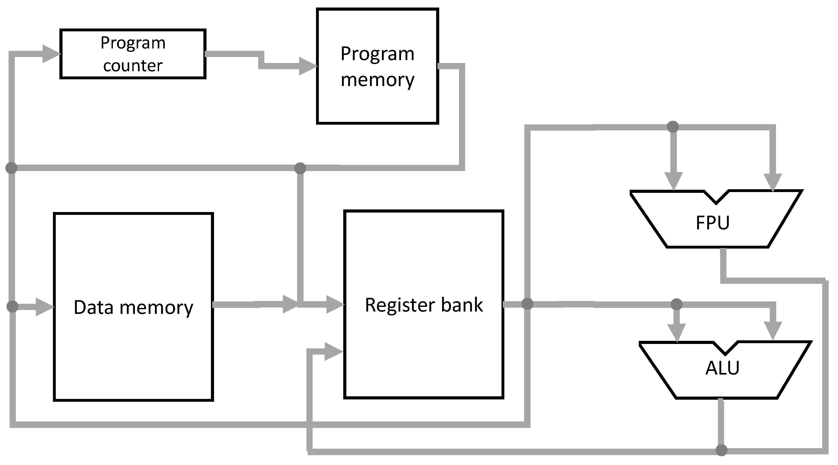
PAMPIUM is a fully customizable microprocessor developed specifically for the design of ASIPs. It is a RISC architecture with a full instruction set composed of 80 instructions. The flexibility of the internal organization allows the configurability for use in different applications since the hardware can be optimally customized for a given design requirement.
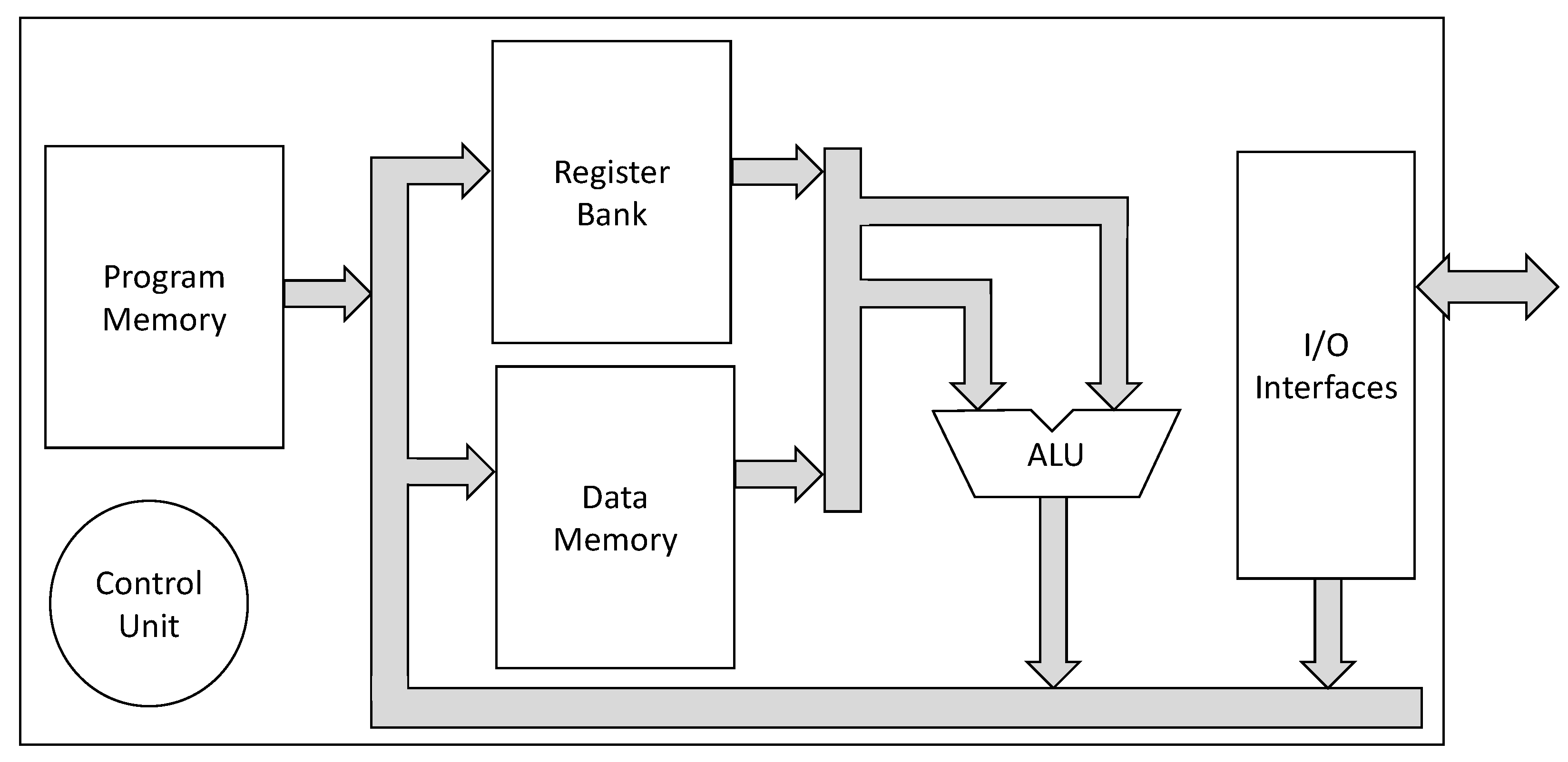
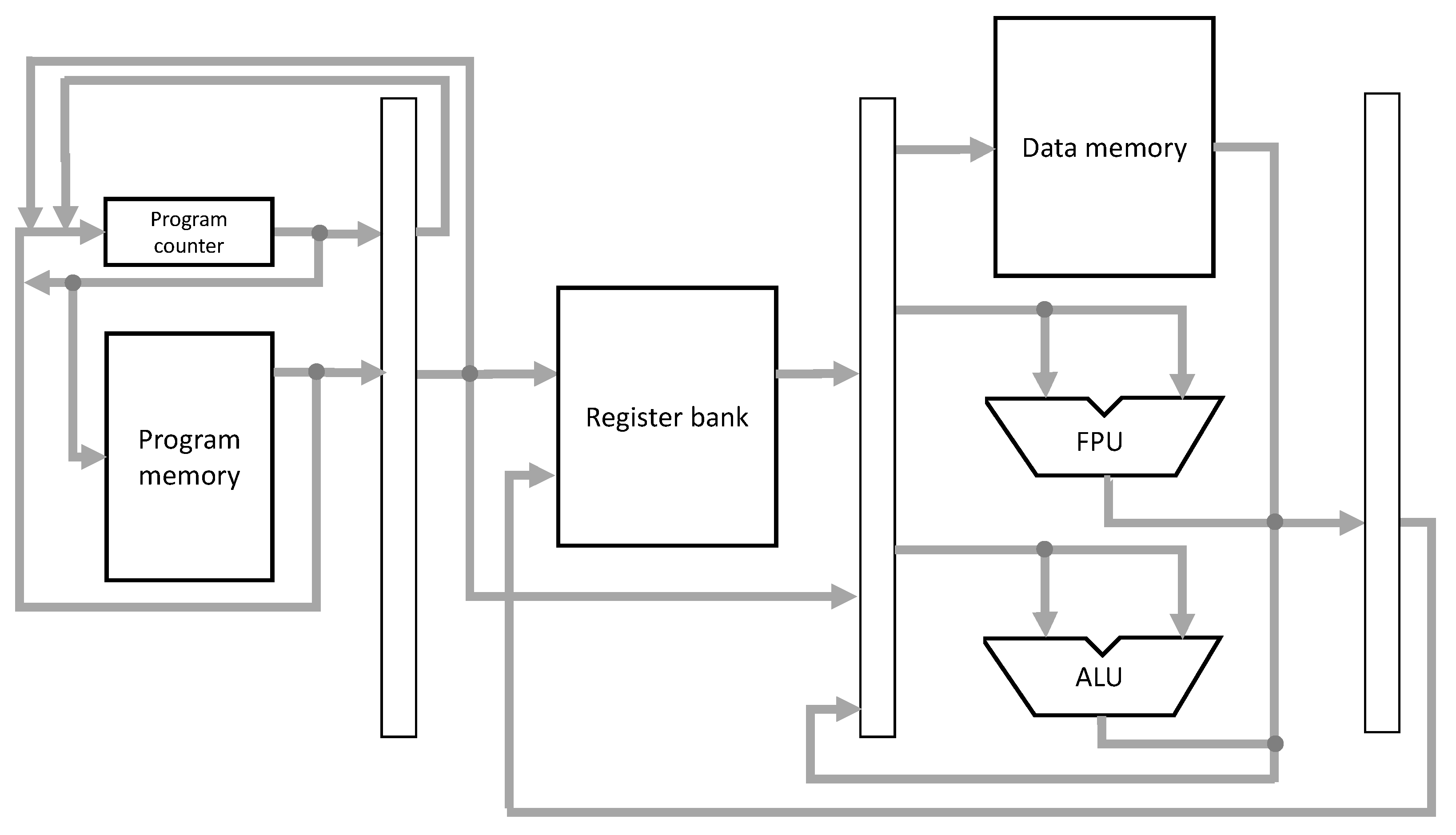
The basic internal organization contains a program memory, a data memory, an arithmetic logic unit (ALU), a register bank, and a control unit. There is the possibility to include
n in-out ports for external communication, according to application requirements. The basic block diagram of this architecture is shown in
Figure 1.
It is possible to configure several aspects, such as the number and types of implemented instructions, number of registers in the register bank, data memory size, type of memory access, instruction word length, data word length, etc. Furthermore, the datapath can be customized by altering the internal organization (monocycle, multi-cycle, pipeline or superscalar). It allows the optimization of the overall characteristics of the microprocessor, resulting in power consumption and silicon area reduction, and performance increase.
It is possible to define customization intervals for some characteristics. For example, the size of the data word is defined by the data type or by the maximum value a variable can achieve (if it is known). Thus, the minimum number of bits for representing an integer variable can be given by the maximum value these variables can achieve in the application.
The size of the instruction word can also be defined by the application. It depends on the number of implemented instructions and registers. It ranges from 9 bits for the basic implementation (small possible ISA) to 40 bits for the full instruction set implementation.
Other parameters, such as the number of registers, depend on the number of variables employed in the application. The register type is given according to the data type (integer, float, etc), which, in its turn, defines the implementation of the functional units (e.g., ALU). Memory access is done according to data type, using indirect addressing, by means of a value given in the instruction word and other stored into a specific register.
PAMPIUM instructions can be divided into three subsets: basic, operative, and data conversion. The basic subset is independent of the data type and contains 13 instructions, as shown in
Table 1.
The operative subset is presented in
Table 2. It is composed of 20 instructions, which can be used for different data types. The “∗” character can be substituted according to the following data types: “F” for operands of type
Float, “I” for
Int, “C” for
Char and “D” for
Double.
The instructions in the data conversion subset convert data from one type to another, according to presented in
Table 3.
From the 80 different instructions available in the PAMPIUM standard ISA, the user can choose to implement only those useful for the target application.
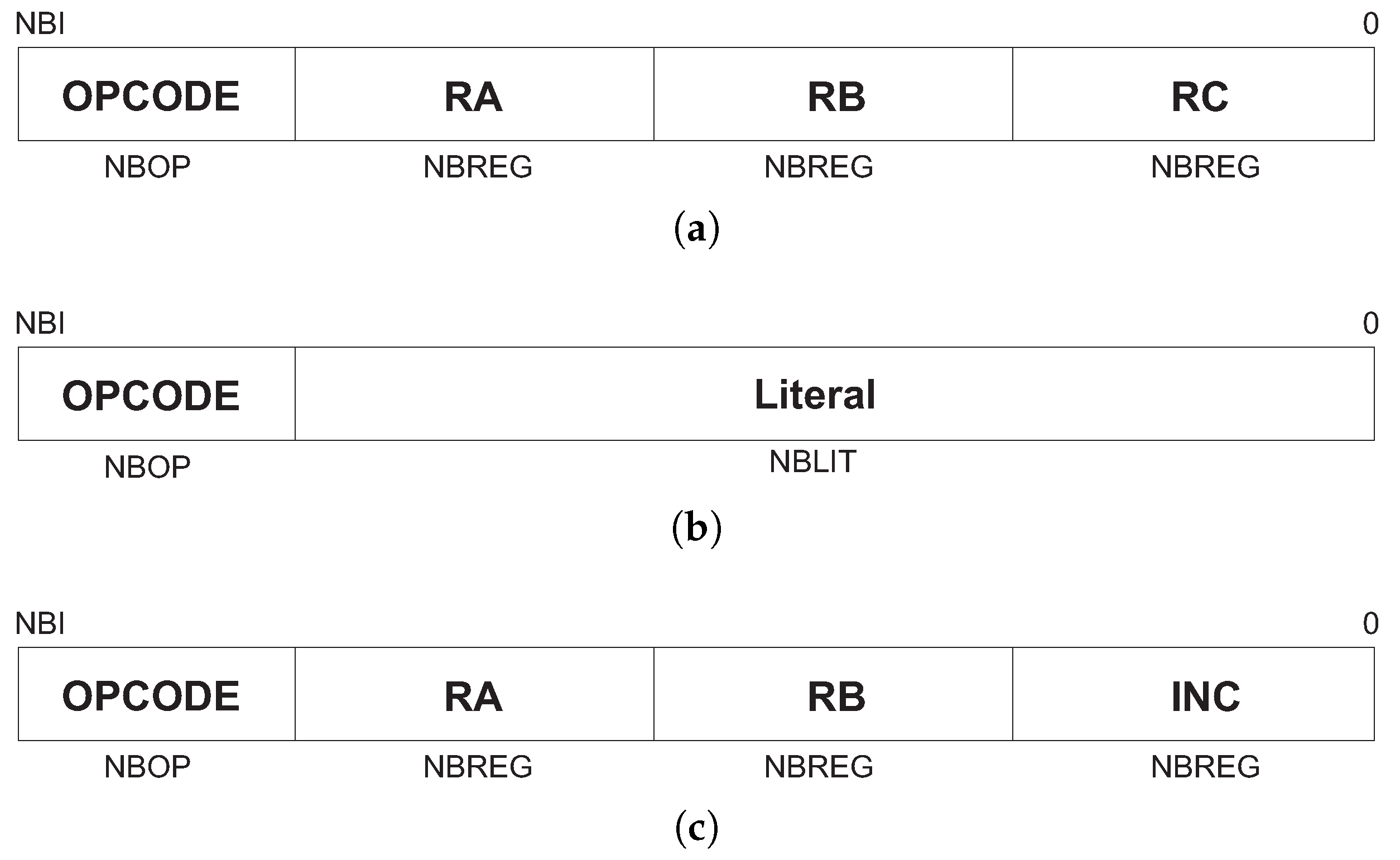
The instructions are represented in three different formats:
R,
L, and
M. The instruction word is divided into two to four fields, according to the format, as can be seen in
Figure 2. The OPCODE field is common to all formats and it stores a unique identification for the instruction. RA, RB, and RC indicate register addresses in the register bank. Fields Literal and INC store constants. The sizes of all fields are configurable, according to the number of implemented instructions and registers.
3.1. Electrical Characterization and Modeling
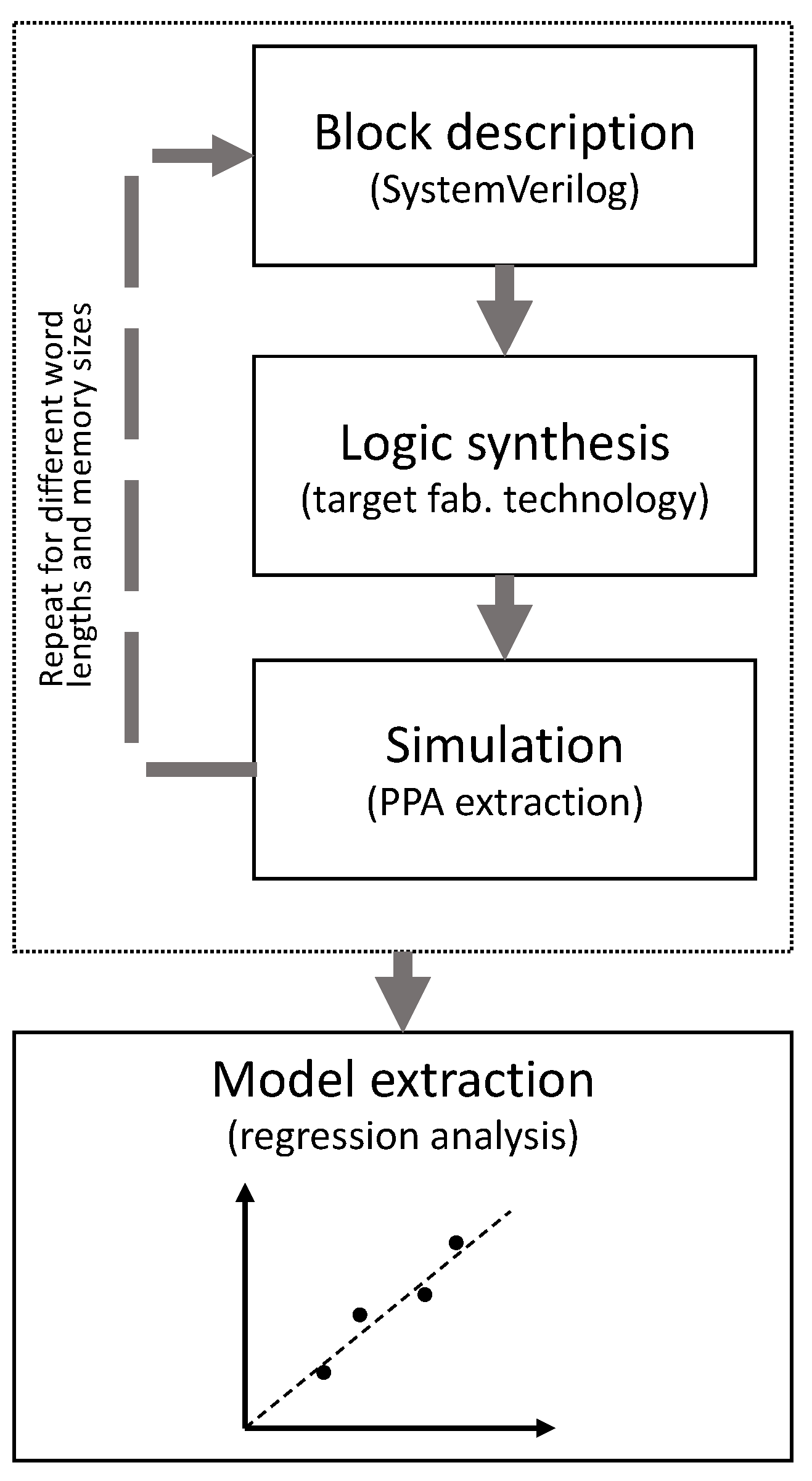
The logic blocks that compose PAMPIUM are electrically characterized in order to provide information to the customized microprocessor generation. This characterization includes the estimation of area, power consumption, and delay time. As each block has configurable specifications, it is important to verify the effect of these specifications on the microprocessor overall performance.
Program memory, register bank, data memory, and arithmetic-logic unit were characterized in 0.18 μm CMOS process technology using Synopsys Design Compiler tool. The data obtained for each block are the circuit area, static power consumption, energy per operation, and delay time. The characterization was performed for several word lengths, with the goal to relate word size to the overall circuit characteristics.
All blocks were described in System Verilog and synthesized to gate level. A vector with 10,000 random values was applied to the input of the circuits for simulation in order to obtain a wide coverage over the entire operating range. For the generation of this vector, we used a random-number generator uniformly distributed over the interval [0, 1]. Binary operands were obtained by multiplying these random numbers by , in which n is the word length.
A model extracted from synthesis results for each building block is used for statistical simulation in which it is possible to determine the more appropriate configuration to be used in the customized microprocessor. These models are based on the simulated results for area, power consumption, delay time, and energy per operation at gate level. Each characteristic is modeled in relation to the size of the block (in the case of memory and register bank) and with respect to instruction or data word size.
Figure 3 depicts the model extraction procedure. The block model can be easily extracted from the results obtained by the logic synthesis for different configurations. For example, the area occupied by the program memory is estimated based on the number of instructions it contains and on the instruction word length. A set of synthesis points is generated for a given range in order to evaluate the behavior of this characteristic. So, regression analysis is used to fit a predictive model from the observed points, which provides a generic function of the memory silicon area in relation to the instruction length and to the program size. This model is dependent on the target fabrication process, since the logic synthesis requires information about the fabrication technology. The linear model is used when the modeled characteristic approximates the linear behavior, which happens in most of the situations. Otherwise, other types of approximations can be used that best fit, such as logarithm or exponential functions.
By means of statistical simulation, it is possible to determine the more appropriate configuration of each block to be used in the customized microprocessor. Moreover, the optimum word length can be estimated. The generated microprocessor can have monocycle, pipeline, or superscalar organization, according to the performance estimated by each compounding block and to the design goals defined by the user. The next subsections describe the characterization and modeling of the main PAMPIUM building blocks.
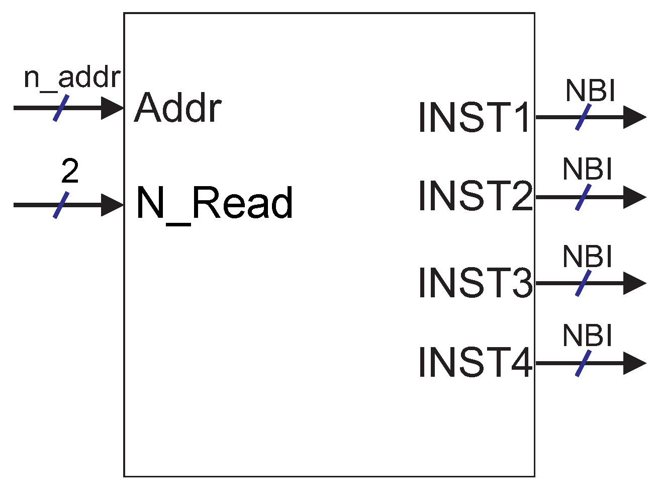
3.1.1. Program Memory
The program memory is a read-only memory for storing program instructions. Its size is determined by the instruction word length and by the size of the application program. The instruction word length can vary, depending on the quantity of registers in the register bank and on the number of different instructions implemented in the customized microprocessor.
Figure 4 presents the logic block of the program memory. The length of input
Addr (address of the current instruction) is proportional to log base two of the number of instructions stored in the program memory. The input
N_Read indicates how many instructions should be read simultaneously at the output (available only in the superscalar version). Outputs
INST,
INST2,
INST3 and
INST4 have the length equal to the instruction word.
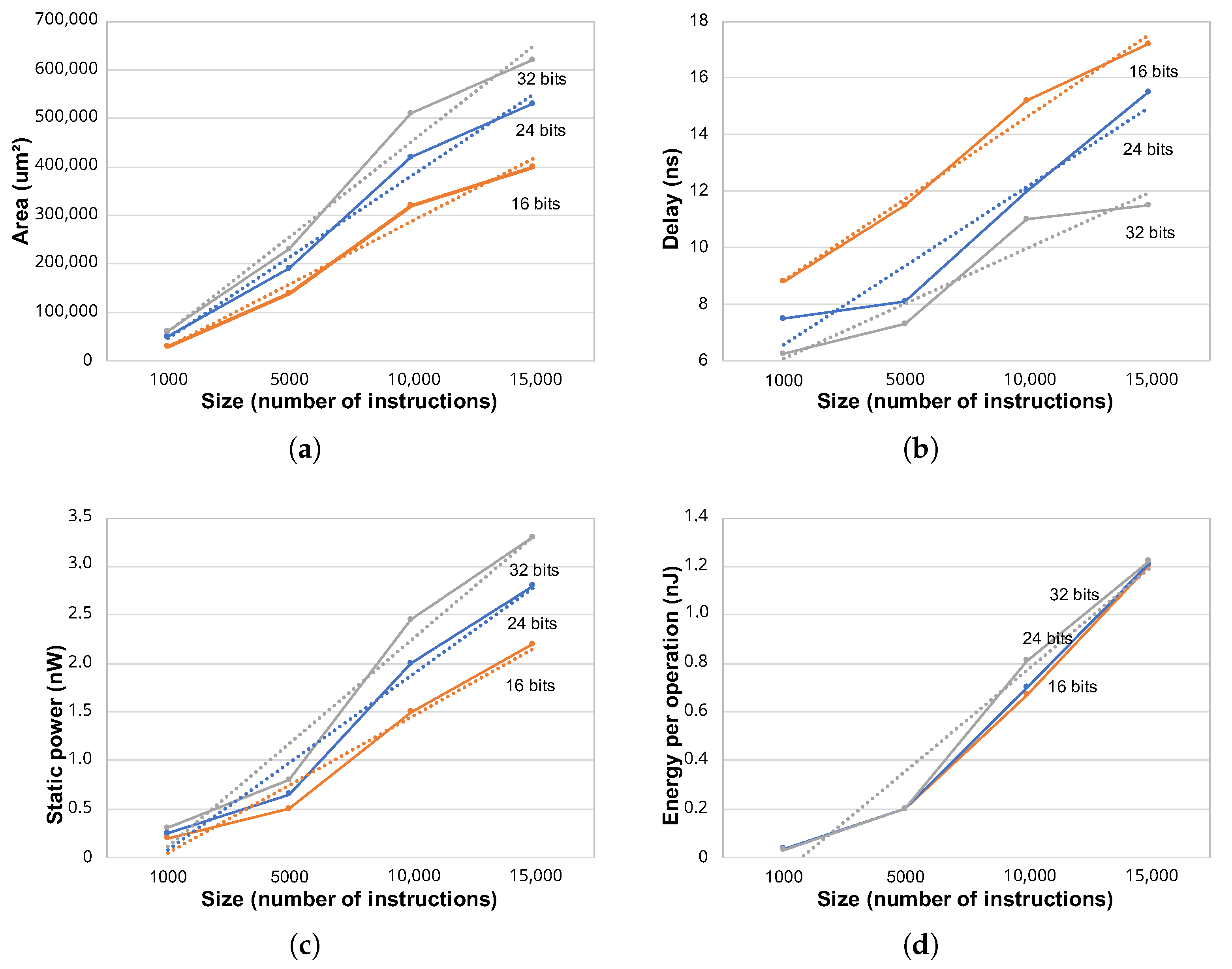
Figure 5 shows the estimation of area, delay, static power and energy per operation (instruction reading) in terms of the length of the instruction word (16, 24 and 32 bits) and of the memory size. It is possible to verify that all characteristics with respect to the number of instructions can be roughly approximated by a linear trend line, thus indicating a clear linear behavior, although a small non-linearity appears. It provides an intuitive scenario for the user, which can easily estimate the effect of reducing or increasing the number of instructions in the program memory. The area of the program memory increases with the number of instructions, as expected (
Figure 5a). More instructions mean more bits to be stored in the memory matrix, but additional resources such as line and column decoders, as well as routing, are also necessary. The reading latency (delay in
Figure 5b) also increases with the number of instructions. It is caused by the additional routing, which increases the parasitic capacitance of bit lines, slowing down the reading procedure. Line and column decoders also become slower with size, contributing to the performance loss of the memory unit. The same occurs to the static power consumption (
Figure 5c) and the energy per operation (
Figure 5d). An increase in the number of logic elements results in a growing static power consumption and in more energy expended for executing a single memory reading operation.
Similar behavior is observed in the program memory characteristics with respect to the size of the instruction word. They present a well-defined proportional variation for instructions with 16, 24, and 32 bits, with the exception of energy per operation, which is not significantly affected by the number of bits in the instruction word.
3.1.2. Register Bank
The number of registers in the register bank is proportional to the number of variables in the application. The length of each register is determined in order to represent the entire range of values that the variables can achieve.
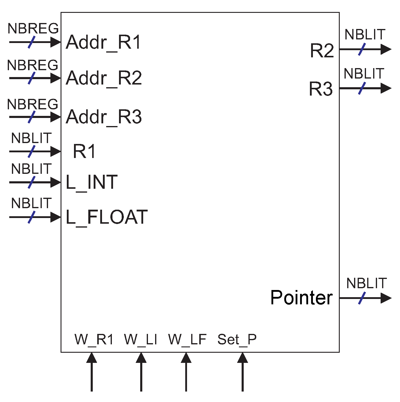
Figure 6 presents the logic block of the register bank for monocycle and pipeline versions. It is possible to simultaneously write data in a register (
R1) and read two other registers (
R2 and
R3). Input signals
Addr_R1,
Addr_R2 and
Addr_R3 represent the addresses of these registers, respectively.
The control signal Set_P and the output signal Pointer are implemented if data memory read and write instructions are implemented in the instruction set. Control signals W_LI and W_LF are implemented only if there are instructions for writing integer and floating point literals on registers. In this case, these literals appear at inputs L_INT and L_FLOAT, respectively.
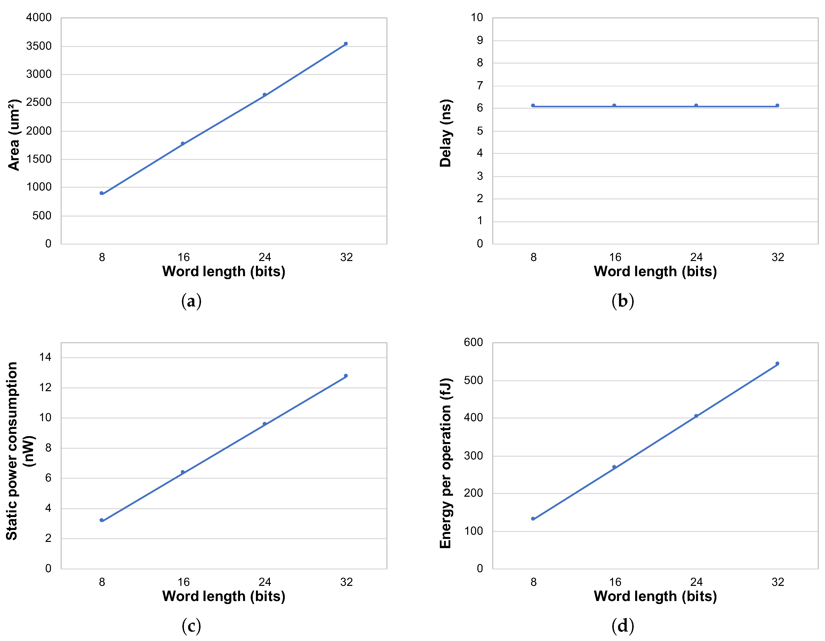
The characteristics of the register bank are affected by the number of implemented registers. Thus, the final results for area, power consumption, and delay depend on the number of registers and on the word length of each register.
Figure 7 presents the influence of the word length over the register bank characteristics. It is possible to notice the linear relationship of area, power consumption, and energy per operation with respect to data word length. On the other side, the delay is not affected by the number of bits in the word length.
3.1.3. Floating Point Unit
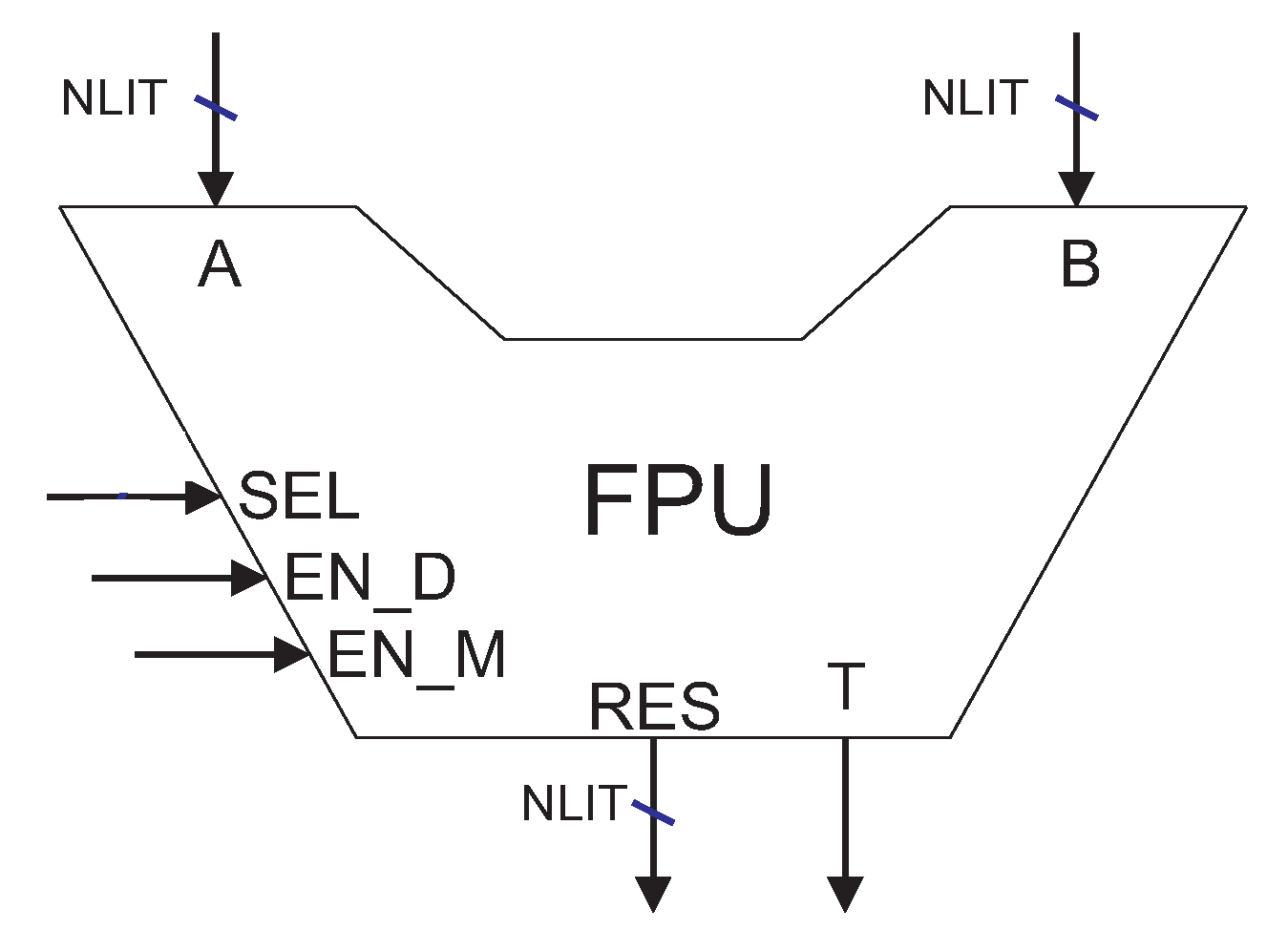
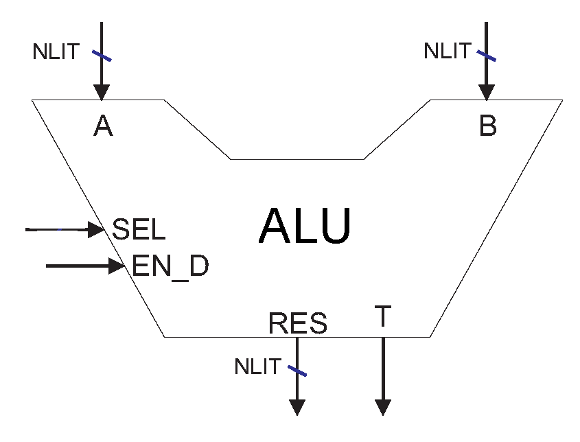
The implementation of the floating point unit (FPU) depends on the number of bits for representing the mantissa and the exponent of the floating point number. The overall block size is related to the number of implemented floating point arithmetic operations, which, in turn, are determined by the existence of the respective operation in the instruction set of the customized microprocessor.
Figure 8 presents the logic block of the FPU, in which
A and
B are the input operands,
RES is the output result and
SEL is a control signal indicating the operation to be performed (sum, subtraction, multiplication or division).
Signals EN_M and EN_D enable the start of a multicycle multiplication and division operation, respectively, and signal T indicates the end of a multicycle operation. They are implemented only in case of the existence of multicycle multipliers or dividers.
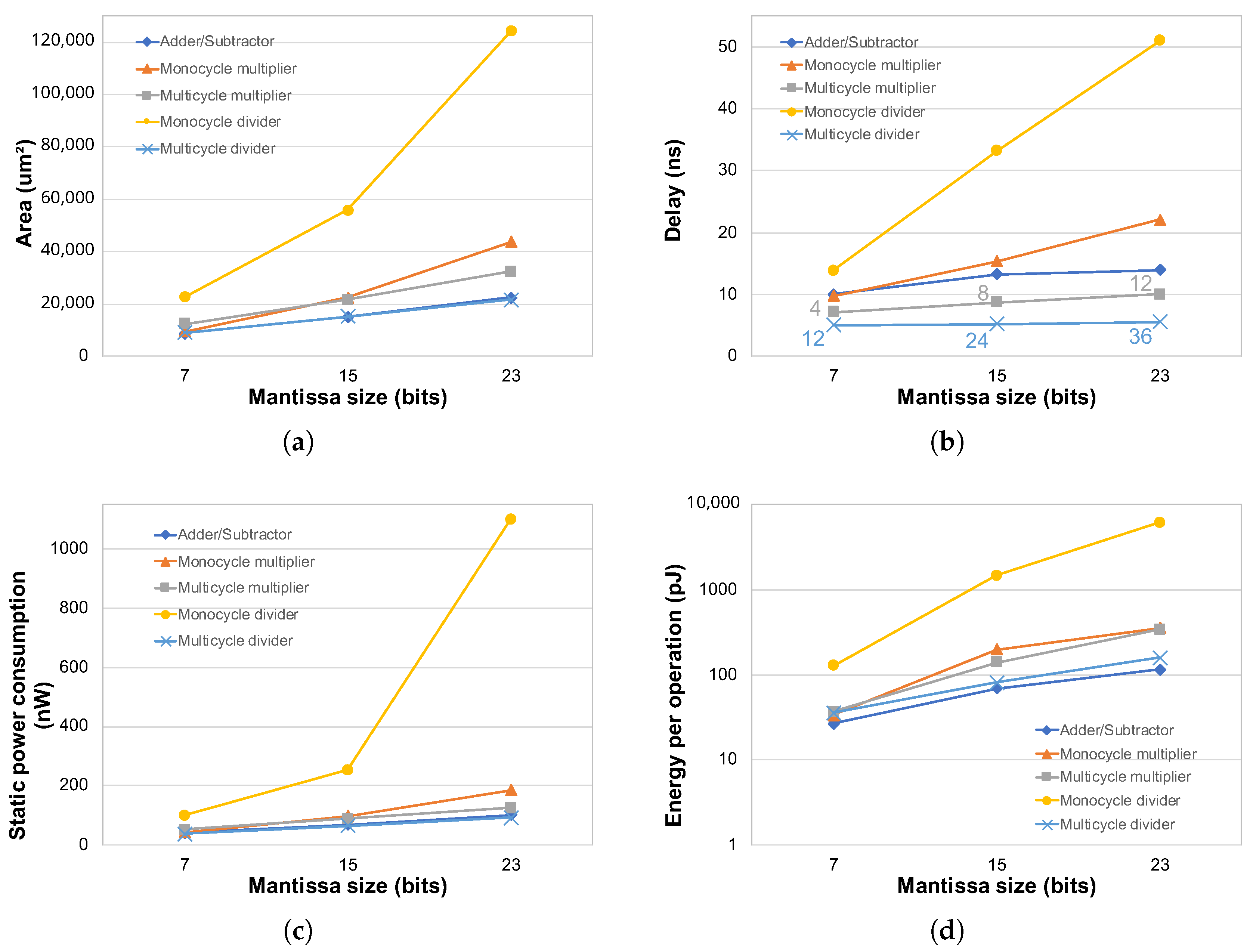
The electrical characterization of this block was achieved by simulation with the number of bits of the mantissa varying from 7 to 23 while keeping the exponent size constant with 8 bits. The following arithmetic blocks are available for implementation in the PAMPIUM: floating point adder, floating point multiplier (monocycle and multicycle versions), and floating point divider (monocycle and multicycle versions).
Figure 9 shows the simulation results at gate level for these blocks. They present a roughly linear growth for area, delay, and static power consumption with respect to the number of bits in the mantissa. The energy per operation exhibits a near logarithm behavior in relation to data word length for all arithmetic blocks, so it is modeled as a logarithm function of mantissa size. For the multicycle versions, the number of cycles to execute an arithmetical operation depends on several factors, for example, the number of bits
1 and the absolute value of the operands. Thus, this estimative was determined by the average of 10,000 randomly selected input operands along the operation range. The resulting average cycles are indicated in
Figure 9b and it also presents a linear behavior in relation to the mantissa size.
3.1.4. Integer Arithmetic Unit
The integer arithmetic unit includes operations performed between registers of integer type. The word length is determined by the size of the largest register of this type.
Figure 10 presents this logic block. Operands
A and
B perform the arithmetic operation determined by the control signal
SEL and the result is available at the output
RES. Signals
EN_D, which enables the execution of the multicycle division, and
T, which indicates the end of the operation, are implemented only in case of the use of multicycle division. The arithmetic blocks that compose the integer arithmetic unit are implemented according to the existence of the operation in the customized instruction set.
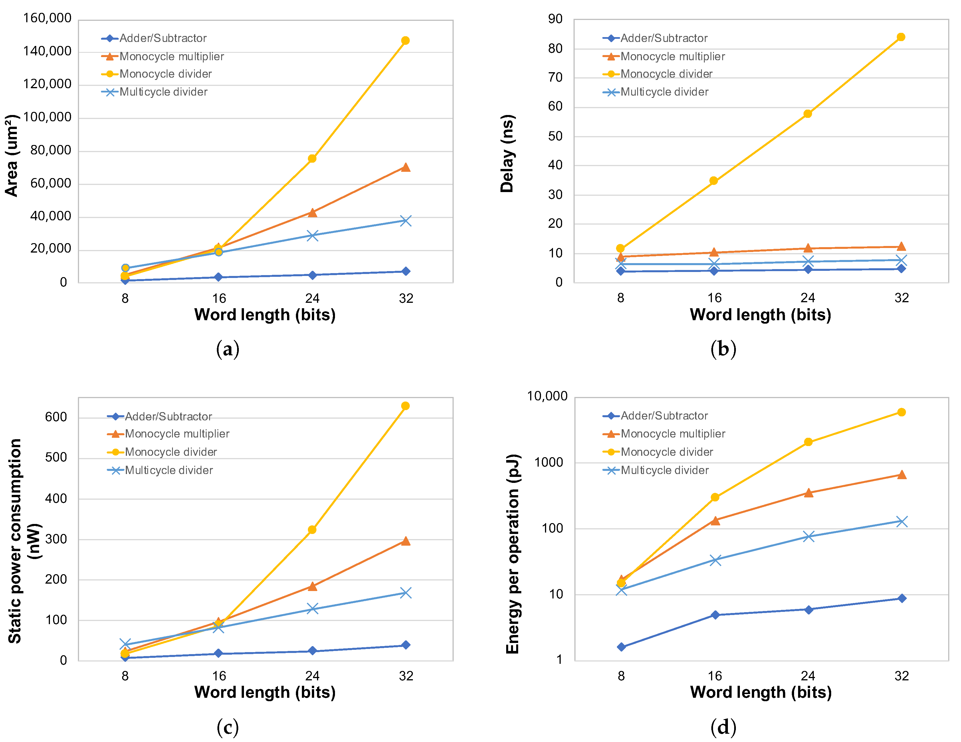
The electrical characterization was performed for operands with a word length from 8 to 32 bits.
Figure 11 presents results for area, delay, static power, and energy per operation for the adder/subtractor, multiplier, and divider blocks in relation to the data word length. The divider has monocycle and multicycle versions. The number of cycles for the execution of an operation in the multicycle divider is dependent on the input values, as for the FPU module. So, the characterization of this block is also the result of a mean of a vector of 10,000 randomly selected operands along the operation range. All electrical characteristics present a near-linear increase as the number of bits of the operands increase, so the model is extracted as a linear function of data length. The number of cycles necessary to perform a division also increases linearly in relation to the word length. Simulation results presented an average number of 5, 7, 9, and 11 cycles for word lengths of 8, 16, 24, and 32 bits, respectively.
3.2. PAMPIUM Monocycle
The monocycle version of PAMPIUM is composed of the following main logic blocks: program memory, program counter, register bank, and control unit. The remaining blocks are added according to the demand of the target application, including data memory, integer and floating point arithmetic units, and external memory interface.
Figure 12 depicts a simplified view of the internal organization of the monocycle version of PAMPIUM. The control block was not shown for better visualization. The datapath is very simple. All instructions are executed in a single clock cycle. This microprocessor is indicated for applications with hard area constraints and relaxed performance requirements. The critical path is determined by the existence and size of the logic blocks, which are implemented according to the customized ISA.
3.3. PAMPIUM Pipeline
The pipeline version is based on the monocycle version, but with instruction parallelization. The datapath is divided into four stages: instruction fetch, data fetch, execution and storage. Pipeline registers must be added between the stages, as well as a hazard control unit.
Figure 13 presents a simplified internal organization of the pipeline version of PAMPIUM.
The main logic blocks present in this version are the same as in the monocycle version. Some multiplexers need to be added to select the correct datapath in case of data hazard. The internal organization of the processor prevents the existence of structural hazards, because each instruction step is executed at a different stage with independent modules, and the execution automatically freezes in case of data dependency.
Interruptions in the pipeline flow can also occur caused by conditional branches, which are calculated in the second pipeline stage (data fetch).
The presence of pipeline registers represents a huge impact on the microprocessor characteristics. The bigger the data word length, the bigger the effect of registers over circuit area and on power consumption. On the other side, the pipeline organization provides advantages in processing performance, increasing data throughput. This type of organization is indicated for applications that require an equilibrium between power consumption and performance.
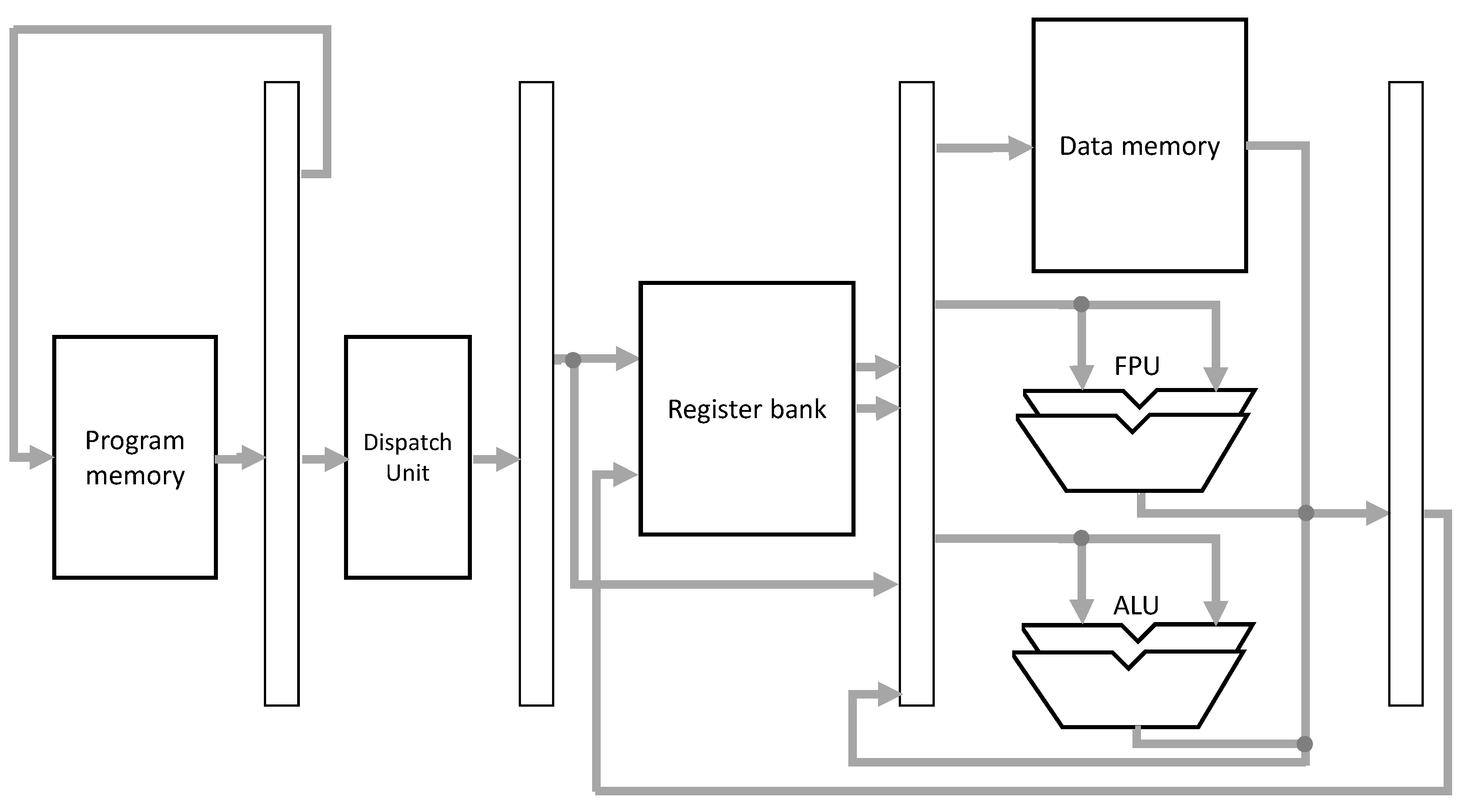
3.4. PAMPIUM Superscalar
The superscalar version of PAMPIUM presents higher level of parallelism than the pipeline version, including datapath and instruction level parallelism. It presents eight different datapaths, providing the possibility to execute in parallel the following operations: one integer instruction, the most used integer instruction, one floating point instruction, the most used floating point instruction, one integer literal instruction, one floating point literal instruction, one memory access instruction and one pointer definition instruction.
Figure 14 presents the hardware organization for the PAMPIUM superscalar version.
The implemented version can execute up to four instructions per clock cycle. For this, the Program Memory must read up to four instructions simultaneously. The datapath is complex in order to deal with the high number of data hazard possibilities, demanding more pipeline registers, which increases circuit area. However, the parallel execution increases the energetic density, making this version suitable for high performance applications.
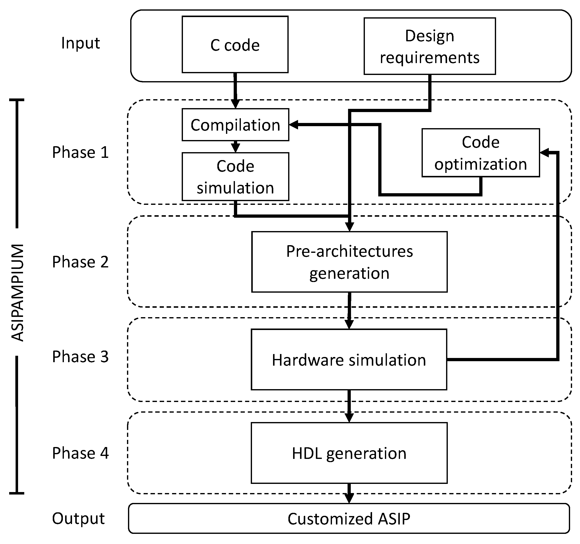
4. ASIPAMPIUM Tool
The EDA tool for semi-automatic ASIP design proposed in this work, called ASIPAMPIUM, receives as input an application code in C language and performs analysis and simulation in order to guide the user to the generation of an optimized microprocessor tailored for that application. Circuit area, power consumption, processing time, or a combination of these, can be set as the design objective.
The design flow is shown in
Figure 15. It can be divided into four phases [
21].
In Phase 1 the application code is compiled in order to identify the necessary hardware operations. The main functional units are identified based on software requirements, including adder, multiplier, divider, memory access, etc. Software variables are mapped to memory positions after their types, range of values, and vector sizes are estimated by simulation. With this procedure, it is possible to optimize memory units and data word length.
In Phase 2 the overall design strategy is defined, identifying the real-time constraints to be respected in order to comply with the required functionality and general assumptions. The pre-architectures are generated based on templates, which allow the estimation of performance, power consumption, and circuit area for different design strategies. In this phase, the compiled code is mapped to hardware according to the minimum instruction set necessary to execute the application. The knowledge of architectural templates and target application provides useful information for dealing with design trade-offs.
In Phase 3 the profiling of the execution of the application code on the generated ASIPs is generated. Circuit characteristics are explored by interactive evaluation and refinement according to the data generated by hardware simulation. At this point, the designer can interact with the tool to explore different scenarios in terms of micro-architectures, building blocks, and custom ISA levels. This phase is repeated interactively after the modification of the hardware characteristics by the designer, such as the inclusion or removal of instructions in the ISA, the resizing of memory units, and the definition of data word length. The evaluation of execution latency for each operation provides an estimation of maximum operating frequency, as well as power consumption and circuit area. The design flow can be returned to Phase 1 if some possible code optimization is identified.
In Phase 4 the optimized hardware description of the ASIP is generated, which can be synthesized for FPGA or ASIC implementation, according to the application.
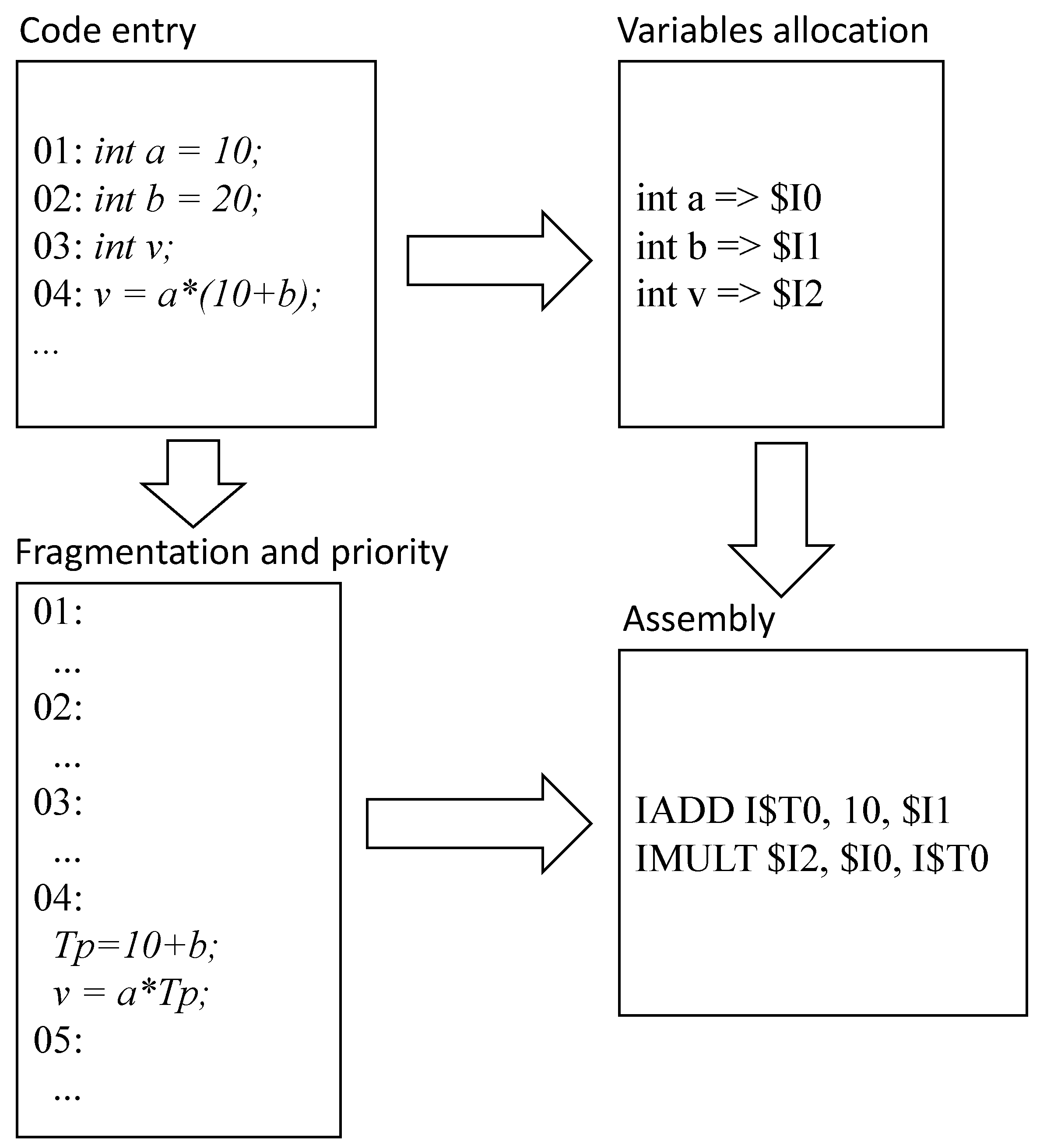
A customized compiler was developed specifically for the PAMPIUM microprocessor. The program described in C language is compiled to PAMPIUM assembly language and the variables are associated to registers according to the data type. At this point, a simulation of the assembly code provides some statistics about program behavior, such as the identification of the most frequent instruction types, the expected range of variables and the required number of registers. These results will guide the synthesis stage for architecture optimization.
Three different circuits are pre-generated according to the monocycle, pipeline and superscalar bases of PAMPIUM. A diagnosis of the specifications generated for these circuits provides information about the best organization that reach the design requirements. Finally, the hardware description of the ASIP is generated in SystemVerilog language [
22], allowing the synthesis for both FPGA and ASIC implementation.
The developed compiler maps the variables according to their types to equivalent registers. The operations are also translated according to the target variable.
Figure 16 shows the compilation flow implemented by the compiler.
The compiler is capable to identify the number, type and scope of the variables. Some temporary variables in different scopes are allocated in order to share the same memory and register positions, thus providing a reduction in terms of required register bank and data memory sizes.
With the assembly simulator tool integrated in the ASIPAMPIUM it is possible to estimate the circuit performance for different hardware configurations, including circuit area, critical path, execution time, and static power consumption. Moreover, the simulator provides information about the minimal instruction set that must be implemented, the frequency of execution of a given instruction, the number of necessary registers, the frequency of memory accesses, the minimum and maximum values of the variables and the number and types of literal inputs in the application. These data provided by the simulator gives to the user a powerful tool for analyzing the trade-offs for circuit implementation.
For each microprocessor version an execution map is generated. It determines the number of executed instructions and the execution order. For the monocycle microprocessor, the execution map provides directly the number of program executions. For the pipeline version, the number of bubbles must be estimated, since it results in additional cycles for the execution of the same program. Pipeline bubbles are consequence of conditional jumps, which deviates the normal program execution flow, or data dependency. A form to reduce the number of bubbles is analyzing the expected result. The most frequent result for the conditional jump deviation test (true or false) is estimated in the simulation and used as standard for predicting if the deviation will occur or not. In the superscalar version the simulator performs an analysis of the parallel execution in the execution map, including bubble insertion analysis. It is possible to execute up to four instructions in parallel in this version. However, it must follow some rules related to data dependency. The superscalar version demands less cycles to execute a program, but it does not mean economy in terms of number of instructions. The execution time can be estimated by multiplying the delay of the critical path to the number of cycles necessary to execute a program.
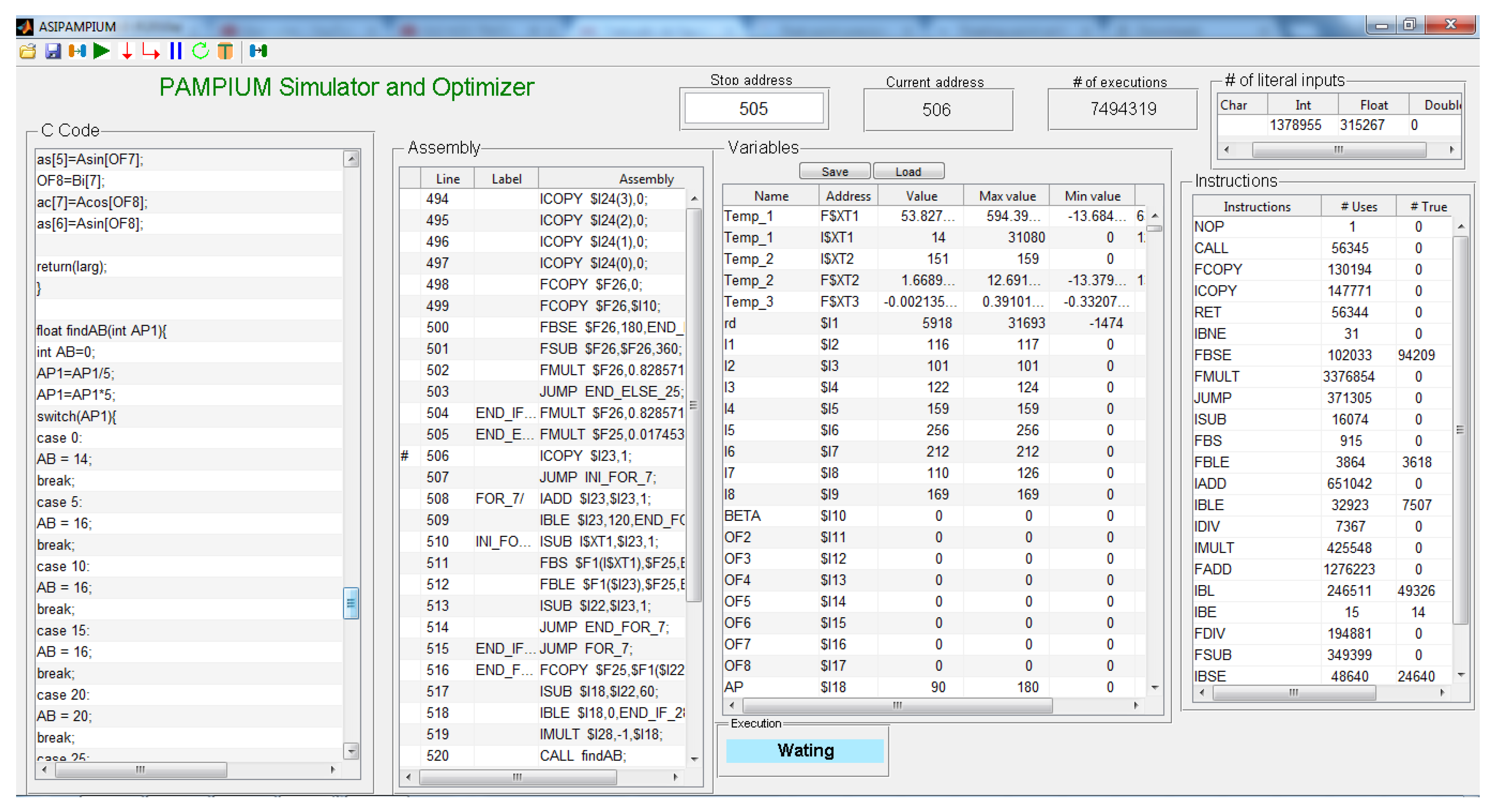
A friendly graphical user interface containing the simulation results and trending graphs is available in the ASIPAMPIUM, helping the user to interpret data and take design decisions, as shown in
Figure 17.
Design Strategies
The customized processor generated by ASIPAMPIUM tool is dependent on the quality of the input user application described in C language. In order to exemplify different optimization strategies, we present an example of the implementation of the cosine function using Taylor series.
The Taylor series that corresponds to the cosine function is given by:
A C code to calculate this series is shown in Algorithm 1.
| Algorithm 1: Cosine function using Taylor series |
 |
The C code is implemented with a loop of type “for” and two subroutines,
fat2 and
exp2. Six iterations were defined for the sum in order to obtain an error below
[
23]. Algorithm 2 presents the PAMPIUM assembly code generated by the compilation, with a total of 52 operations.
| Algorithm 2: PAMPIUM assembly code for Algorithm 1 |
 |
The customized ASIP to implement the cosine function presents a 32-bit fixed and floating point architecture. It is necessary the use of 12 32-bit registers and 5 8-bit registers. The customized instruction set is composed of 20 instructions. The results generated by the ASIPAMPIUM tool for the three PAMPIUM versions are presented in columns 2, 3 and 4 of
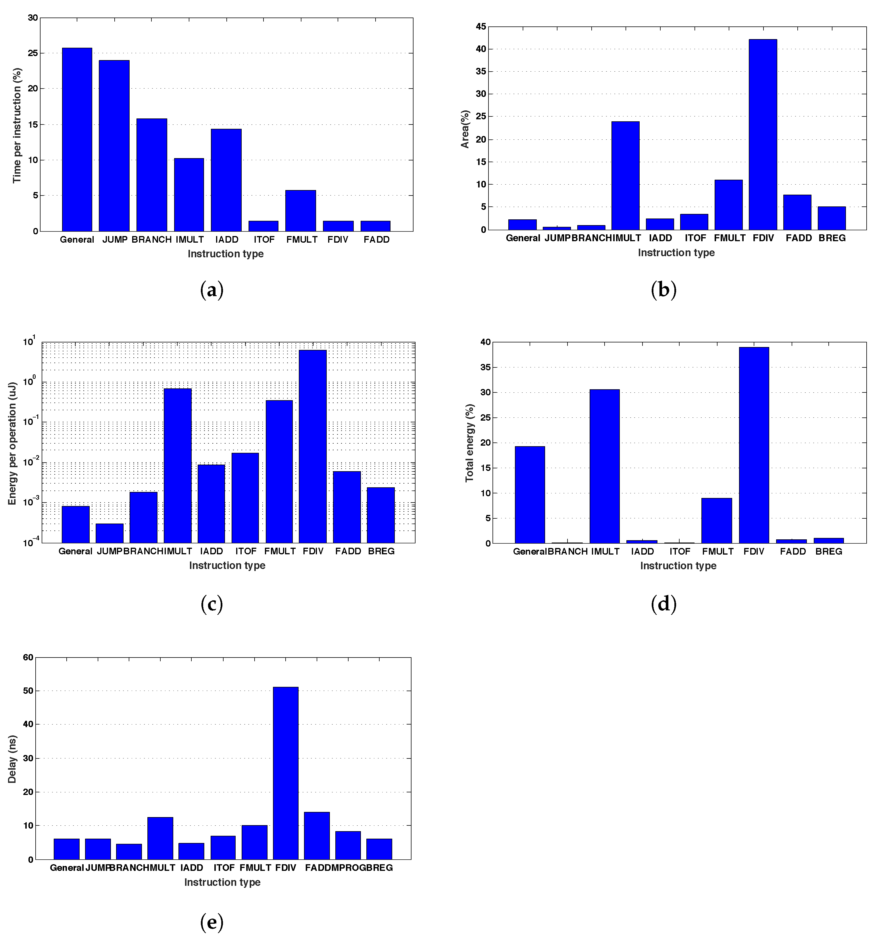
Table 4. It is possible to note that the monocycle version presents smaller area and smaller power consumption in comparison with other versions. However, it presents a slower execution time. As expected, the pipeline version presents intermediate values and the superscalar version has the smaller execution time, but at the expenses of increase in area and power consumption.
Figure 18a presents the total time execution for instruction type. Most of the execution time is spent with general-purpose instructions (literal load,
COPY, etc.) and jump instructions (
JUMP,
CALL,
BLE and
BL), representing about 67% of the total time. Arithmetic instructions, such as
FADD, FDIV and
ITOF represent only 8% of the execution time. So, it is possible to notice that the elimination of loops and subroutines in the C code is mandatory to optimize the total execution time.
Figure 18b depicts the contribution of instruction types over the total microprocessor area. About 43% of the circuit is used by the floating point monocycle division block. The second larger block is the fixed point multiplier, occupying 24% of the circuit area. An optimization in the area could be performed by substituting the divider by its multicycle version—which presents smaller area—or by eliminating any floating point division in the code.
Figure 18c shows the contribution of each instruction type to the circuit power consumption. The block with larger energetic impact is again the monocycle floating point divider, with a total of 6 μJ. This value is very large compared to the remaining blocks, indicating that it can be substituted by the multicycle version, which presents better energetic efficiency.
Figure 18d presents the relative energy consumption for each instruction type. The floating point division is responsible for 39% of the total consumed energy, followed by the fixed point multiplication, with 31%, and the general purpose instructions, with 19%.
The monocycle floating point divider has the larger critical path (about 51 ns), as can be seen in
Figure 18e. The remaining blocks present a critical path around 10 ns, which indicates a balance problem in relation to the instruction delays. It suggests a multicycle implementation for the divider, which allows the increasing in the microprocessor operation frequency.
So, rewriting the application code it is possible to improve the hardware performance in different aspects. The floating point division is used only few times in the algorithm, but presents a high impact on power consumption, area and delay. However, it is not possible to eliminate it, because it is fundamental for the Taylor series calculation. So, the best approach is the substitution of the monocycle divider block by its multicycle version.
Furthermore, most of the execution time is spent with loops and subroutines. The code can be optimized by removing unnecessary loops and by reorganizing functions for calculating exponent and factorial—which can take advantage of previous results for calculation.
Another important aspect which contributes to the circuit performance is the variable type for each operation. Presented results use 12 32-bit registers and the fixed-point numbers are also 32 bits. The factorial calculation generates very high numbers, which requires an increasing in area to represent the operands. As the fixed-point hardware is sized by the largest operand, this function would impact in unnecessary effort for the remaining functions. So, the best option is to change this variable to floating point. Algorithm 3 presents the refactored code with the improvements discussed before.
| Algorithm 3: Optimized cosine function for hardware synthesis |
 |
Columns 5, 6 and 7 of
Table 4 summarizes the new circuit performance, considering code optimization. The values of area, execution time and power consumption were significantly reduced compared to the non-optimized code. Multicycle version presents the smaller area and power consumption (reduction of 42% and 36%, respectively, in comparison to the original monocycle version), while superscalar version presents the best performance in terms of execution time, with a reduction of more than 2x in relation to the original counterpart. This demonstrates that the statistical analysis generated by ASIPAMPIUM tool provides very useful information for the optimization of customized ASIPs.
Design strategies related to C code optimization can be generalized for any application. The elimination of a given arithmetic operation or its substitution by the multicycle version, when possible, can result in great improvements in terms of area and power consumption. The removal of unnecessary loops contributes to the reduction of jump addresses calculation, thus providing advantages in terms of power consumption and performance. The reuse of temporary variables reduces the size of the register bank. Furthermore, the type of numerical variables (integer or floating point) must be evaluated in relation to area, power consumption and performance. However, the application of these strategies depends on design objectives. A careful evaluation of the resulting effect over conflicting requirements is mandatory.
5. Application Example: FFT Synthesis
This section presents the results generated by the ASIPAMPIUM tool for the implementation of a dedicated Fast Fourier Transform (FFT).
The FFT is applied to several data transmission systems. It transforms the data in the time domain to the frequency domain [
24]. This technique is very used for the analysis of the modulation signal and for orthogonal frequency division multiplexing (OFDM), which is the base for different communication systems [
25]. Several digital communication standards, such as ultra-wideband (UWB), worldwide interoperability for microwave access (WiMAX), wireless LAN (WLAN), integrated services digital broadcasting terrestrial (ISDB-T), long-term evolution (LTE), digital video broadcasting (DVB-T), and digital video broadcasting second generation terrestrial (DVB-T2) adopt OFDM systems for the processing of digital signals [
26].
The discrete-time Fourier transform
of a finite number of points
, where
, is calculated as:
The coefficient
is a complex number represented by the following exponential equation:
In general, the complexity of FFT evaluation can be reduced to two sums of
M and
L coefficients, where the number of points
N is given by
. So,
where
.
A radix-16 algorithm was implemented, using variables of type float for the calculation of the FFT points and variables of type int for the calculation of the FFT indexes. The algorithm is able to calculate an FFT with N points, in which N is a power of 2 from 32 to 2048. A 16-point butterfly was optimized in order to reduce the number of operations and variables.
With this algorithm, it is necessary to execute 1024 accesses to data memory and 512 floating point multiplications and sums for each butterfly, not considering the calculation of the indexes.
In order to reduce even more the computational effort, the calculation is divided into real and imaginary parts, where . With this simplification, it is possible to reuse some twiddle factors. The number of data memory accesses per butterfly is reduced to only 16 (the size of the butterfly), the number of floating point multiplications to 48 (since some twiddle factors are zero or repeated), and the number of sums to 368, thus minimizing the computational effort to calculate the FFT of a discrete signal.
For example, for a complete calculation of a 2048-points FFT, it is necessary memory accesses using the described methodology. Otherwise, without this technique, it would be necessary memory accesses. Thus, the number of memory accesses is reduced by 64 times.
The developed program has about 300 lines of C code, and its translation to Assembly resulted in 3071 operations. Only 23 different instructions were necessary to implement the code, from the 80 available in the PAMPIUM architecture. The most frequent instruction is the floating point add (FADD). The simulations and analyses performed by the ASIPAMPIUM tool last about 3 h in an i7-3770 CPU @ 3.40 GHz.
The resulting processor synthesized by the ASIPAMPIUM tool has 9 16-bit integer registers, 81 32-bit floating point registers, and 6 8-bit registers.
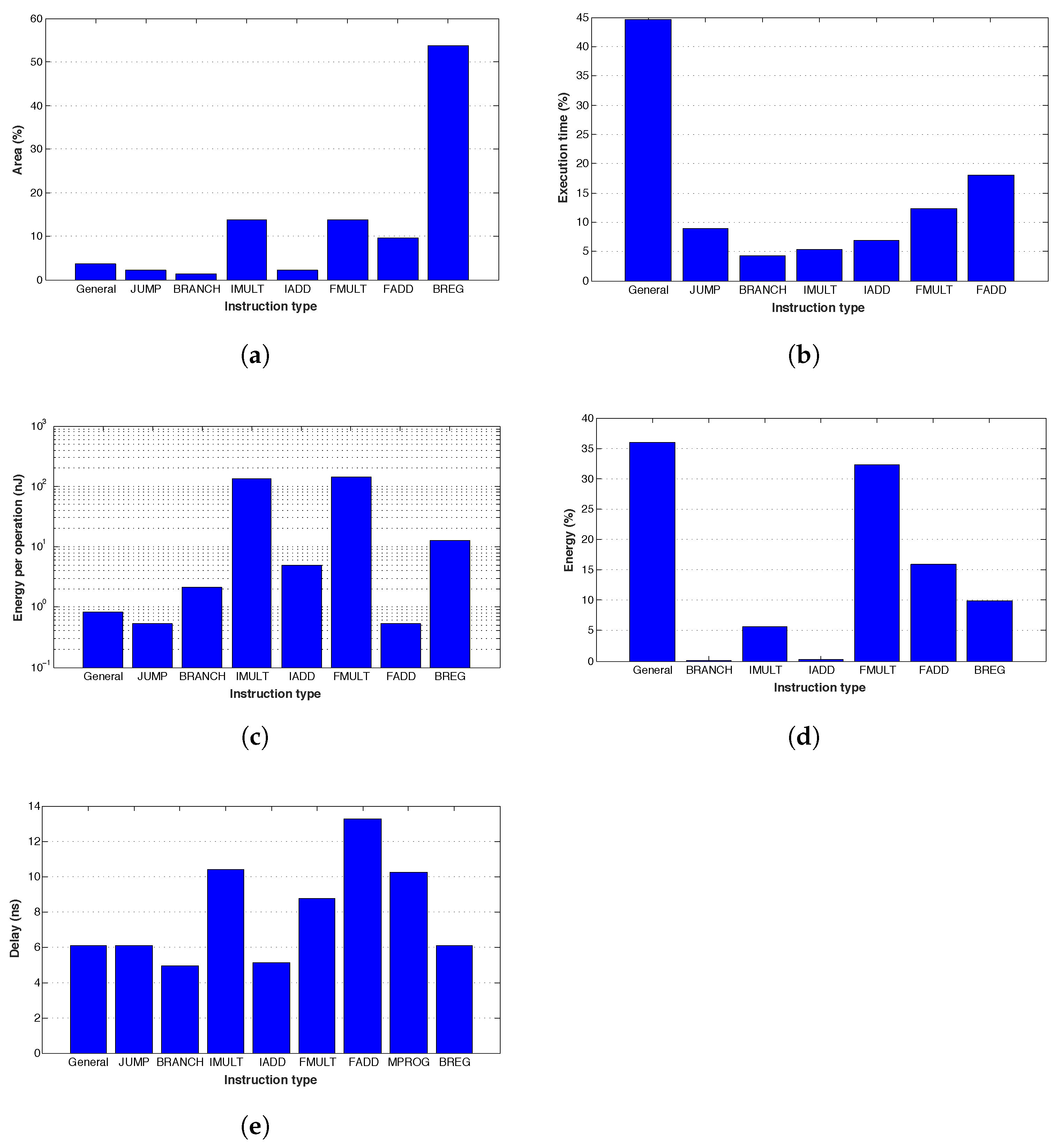
Figure 19a presents the relative area occupied by each logic block. The register bank block is the most area consuming, due to the high number of registers to store the program variables. So, optimization in terms of circuit area could be obtained by reducing the number of variables in the code.
Figure 19b presents the execution time spent for each instruction type. General type instructions (literal input and data memory access) require about
of the total execution time. The most used arithmetic instruction is the floating point add, demanding
of the execution time. An optimization in the execution time could be obtained by reducing the number of data memory access or the literal inputs.
Figure 19c presents the energy by operation consumed by the implemented logic blocks, showing that integer and floating point multiplication are the most energy-consuming instructions.
The relative energy consumption of each logic block in relation to the overall microprocessor consumption is presented in
Figure 19d. The general purpose instructions are responsible for most of the energy consumed in an FFT calculation, demanding
of the total energy.
In terms of delay, the floating point add is the slower block, as depicted in
Figure 19e. It can be seen that some optimizations can be achieved for the FFT calculation in the code domain, mainly to reduce the number of arithmetical operations.
The identification of the common variables in the algorithm and the reuse of values generated by some arithmetical operations are key for reducing the time- and area-consuming instructions. So, the number of floating point sums and multiplications inside the butterfly can be reduced to 94 and 18, respectively, as well as the number of memory accesses can be minimized to 16.
After optimizing the code, we generated two versions of the PAMPIUM processor: a multicycle version, called PAMPIUM_M, optimized in terms of circuit area and power consumption; and a superscalar version, called PAMPIUM_S, developed to achieve the best possible performance.
In order to compare the obtained results with other works described in the literature, we adopt as a figure of merit the normalized energy
and area
[
27]. Both are referred to 65 nm technology node and take into account the voltage scaling:
Here, P is the power consumption, is the clock period, is the number of clock cycles necessary to calculate the FFT, is the voltage supply and A is the circuit area.
The obtained results are compared to the work in [
28], which describes the implementation of a module to perform FFT calculation using the CORDIC (
Coordinate Rotation Digital Computer) method using Xilinx Virtex-5 FPGA platform.
Table 5 presents the results and the comparison with the versions generated by ASIPAMPIUM, which are implemented in Altera Stratix IV FPGA. These versions are based on multicycle (
PAMPIUM_M) and superscalar (
PAMPIUM_S) architectures. The
PAMPIUM_M version presents a smaller area with respect to [
28] (smaller number of look-up tables—LUTs), but at the expense of smaller operation frequency. The
PAMPIUM_S version, on the other side, is faster but demands a higher number of LUTs. It can be seen that there is a trade-off between area and performance in the FPGA implementation.
It is also possible to compare the results obtained by the physical synthesis of the
PAMPIUM_M and
PAMPIUM_S in 180 nm fabrication technology with other state-of-the-art works in the literature. The work described in [
13] presents a hardware description language of the LISA machine for the implementation of an ASIP. Using software tools for design, system verification, and implementation, the proposed design flow allows prototyping and testing, aiming to reduce design time and human effort with respect to traditional design methodologies. It presents a case study on a parallel FFT algorithm. In [
26] a reconfigurable process platform is used and a similarity matrix is adopted with the goal to reduce the number of access to the main memory by using a large register file to store intermediate data. In [
29] a radix-4/2 butterfly structure is adopted for exploring the parallelism in the FFT calculation, but it requires more memory accesses. In [
30], four VLIW vias and four tracks in the SIMD architecture are adopted, with different data shuffling modes to improve the FFT transfer rate, aiming to reduce energy consumption.
Table 6 summarizes the comparison between these implementations and the generated PAMPIUM versions using the normalization Equations (
5) and (
6).
We can notice that the multicycle version of PAMPIUM, synthesized for 180 nm technology, presents the smallest circuit area. The operation frequency is lower, due to the smaller parallelism level in comparison to the other implementations. However, the extremely low power consumption of mW indicates the optimization for low-power applications while occupying the smaller silicon area. This version needs 33,600 cycles () to perform the calculation of a 1024-point FFT, which degrades the energy efficiency.
The superscalar version of PAMPIUM, on the other side, presents better energy efficiency compared to the other implementations, while maintaining a small silicon area. It has a power consumption of just mW at an operating frequency of 98 MHz. The instruction-level parallelism reduces the to less than half of the multicycle version.
The good results obtained by the ASIPAMPIUM for the generated ASIPs for implementing the FFT algorithm demonstrate the functionality of the EDA tool. It provides an efficient environment for dealing with design trade-offs in a short design time, generating optimized circuits with a performance comparable to the obtained by other methodologies.
6. Prototyping and Measurement Results
We prototyped a version of PAMPIUM generated by ASIPAMPIUM in order to validate in silicon the complete design methodology implemented with the tool. The central application is presented in
Figure 20, which is a hardware platform for gesture recognition system using accelerometers and gyroscopes for the detection of movements in the x, y, and z axes. The system must read up to six sensors using I2C protocol and transmit the information to a computer through the RS232 serial protocol with a power budget of 50 mW.
The version of the processor, called PAMPIUM IC, was developed using the ASIPAMPIUM tool and the circuit was prototyped in TSMC 0.18 μm technology. To provide the reading of the sensors, three interface modules were implemented, compatible with I2C protocol [
31].
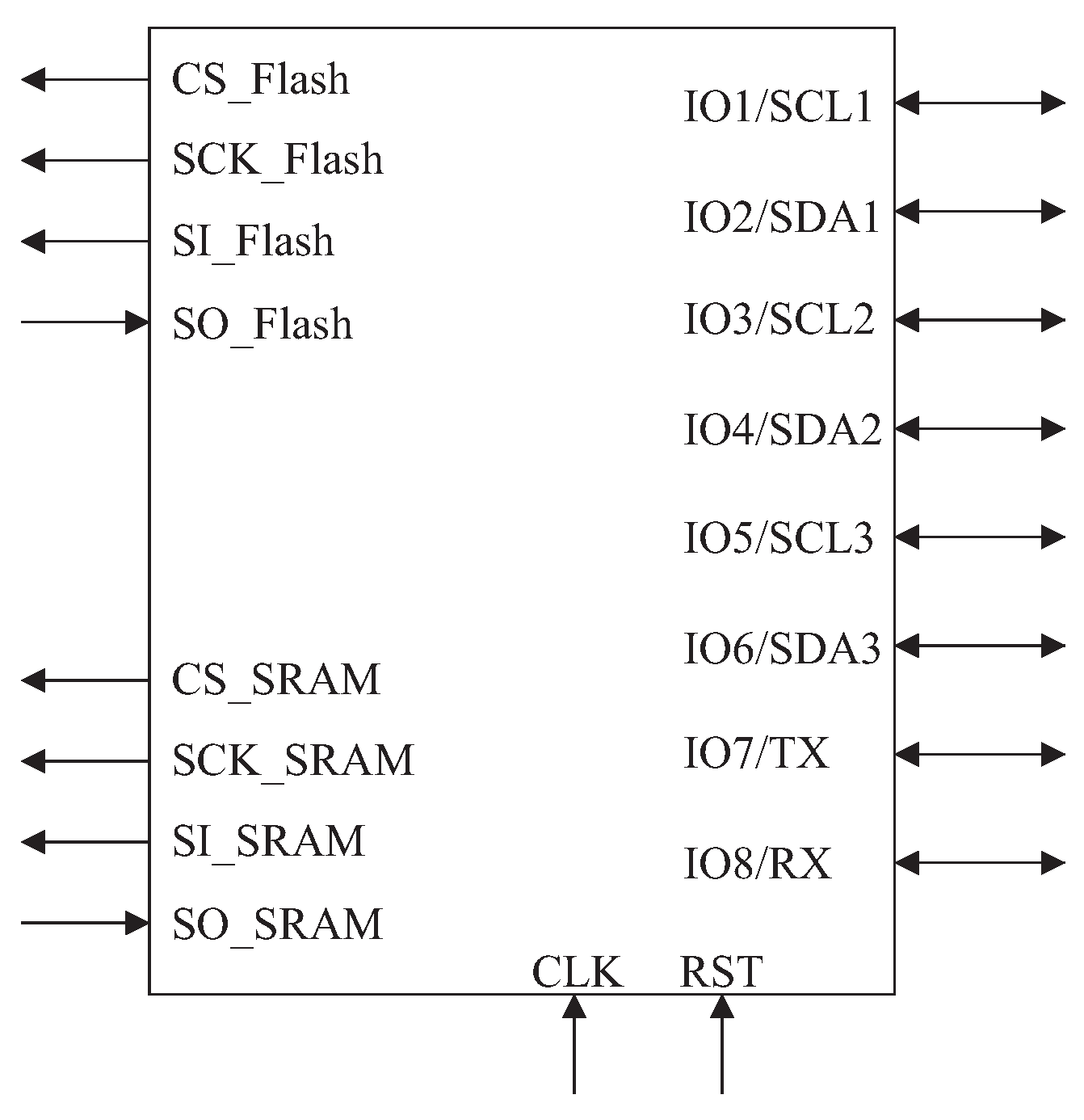
The entire circuit has a hard area constraint of 0.34 mm2, as well as a limit of 20 input/output pins.
Small cache memories are implemented inside the processor, reducing the silicon area. They communicate with data memory and program memory, which are located outside the chip, by means of the SPI protocol.
Logic and physical synthesis of the circuit, as well as simulation, were executed using Synopsys RTL-to-GDSII flow, with the digital logic library provided by the foundry.
A C program was developed for the implementation of three I2C and one RS232 communication module.
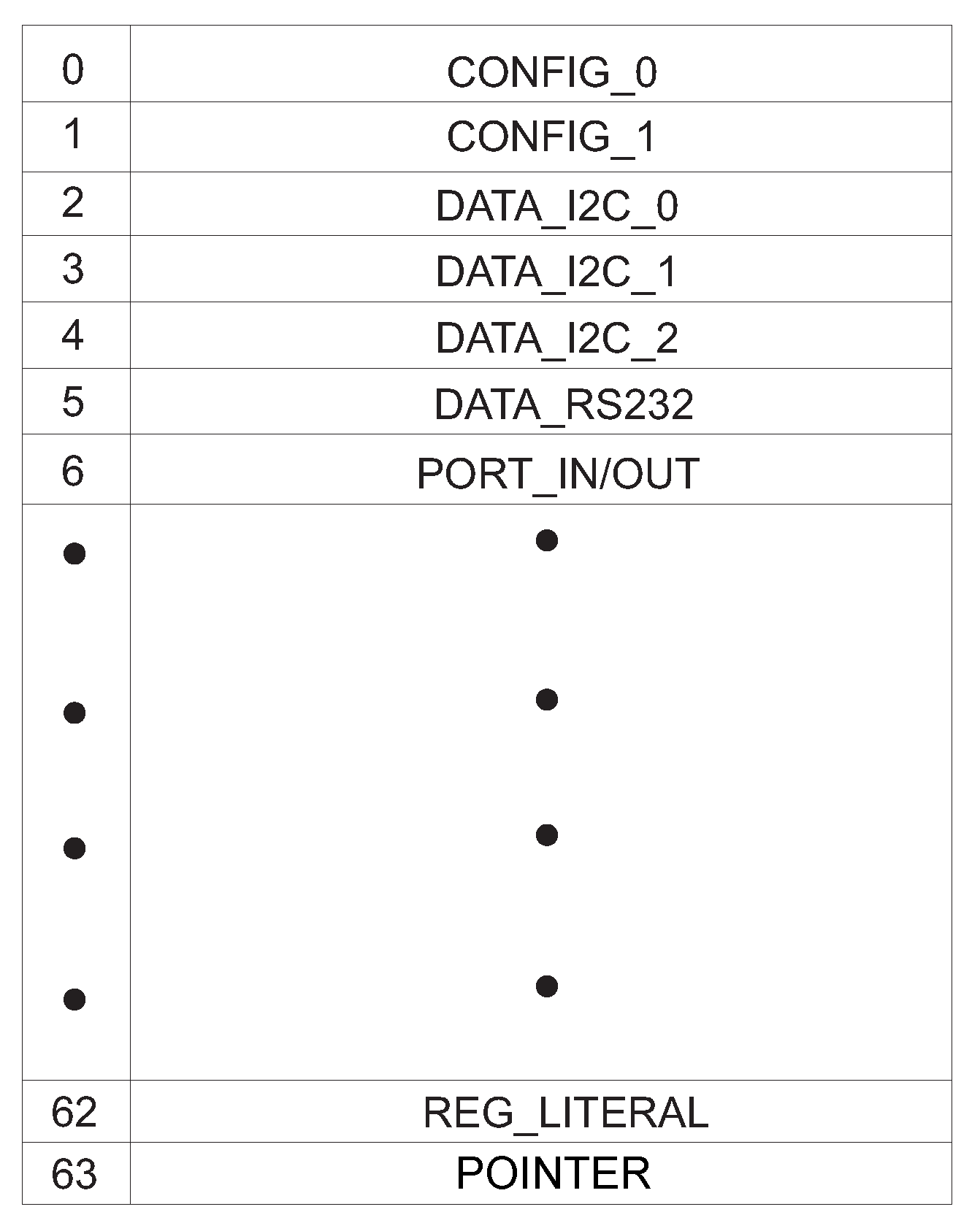
The processor architecture is of integer type, with a data length of 16 bits and an instruction word of 24 bits. It has 64 16-bit registers, 9 of them used specifically for literal input, program memory pointer, and configuration.
Figure 21 presents the implemented register bank.
Registers CONFIG_0 and CONFIG_1 are reserved for the implementation of configuration signals and interruption control. Registers DATA_I2C_0, DATA_I2C_1, DATA_I2C_2 and DATA_RS232 are reserved for the data exchange between the processor and the communication modules. Register PORT_IN/OUT is used for the configuration of directions and values of the input and output pins. Registers REG_LITERAL and POINTER have the function to store the input literal and the data memory pointer, respectively.
The RTL description was divided into two stages. First, the RTL description of the monocycle version of PAMPIUM was generated by the ASIPAMPIUM tool. The processor was optimized for achieving the area constraint. In the second stage, the cache memory was included, as well as the blocks for the interface with RS232 and I2C protocols.
The data cache memory is composed of 16 positions, each one storing a 16-bit word. These positions are divided into four banks. Each bank has a register that store the upper part of the data memory address. So, the accesses performed by the external memory are made in blocks of four consecutive accesses. This strategy maximizes the performance, exploring the local proximity of the data.
The program cache memory is composed of eight positions, each one containing a 24-bit word. Each position has a register for storing its original address. The storing process is made in a sequential form, i.e., the instructions are stored from the lower to the higher address, due to the sequential nature of the program memory. The use of eight store positions allows the execution of small loops without the need to perform additional external loads.
The implementation of the data and program cache memories, with the remaining memory in the external part of the chip communicating by means of SPI protocol, allows the use of only eight input/output pins for data transfer between memory and CPU. With the remaining pins of “clk”, “rst”, “vdd” and “gnd”, and the four communication modules, the overall circuit needs a total of 20 input/output pins.
Figure 22 presents the final pin scheme of the customized processor.
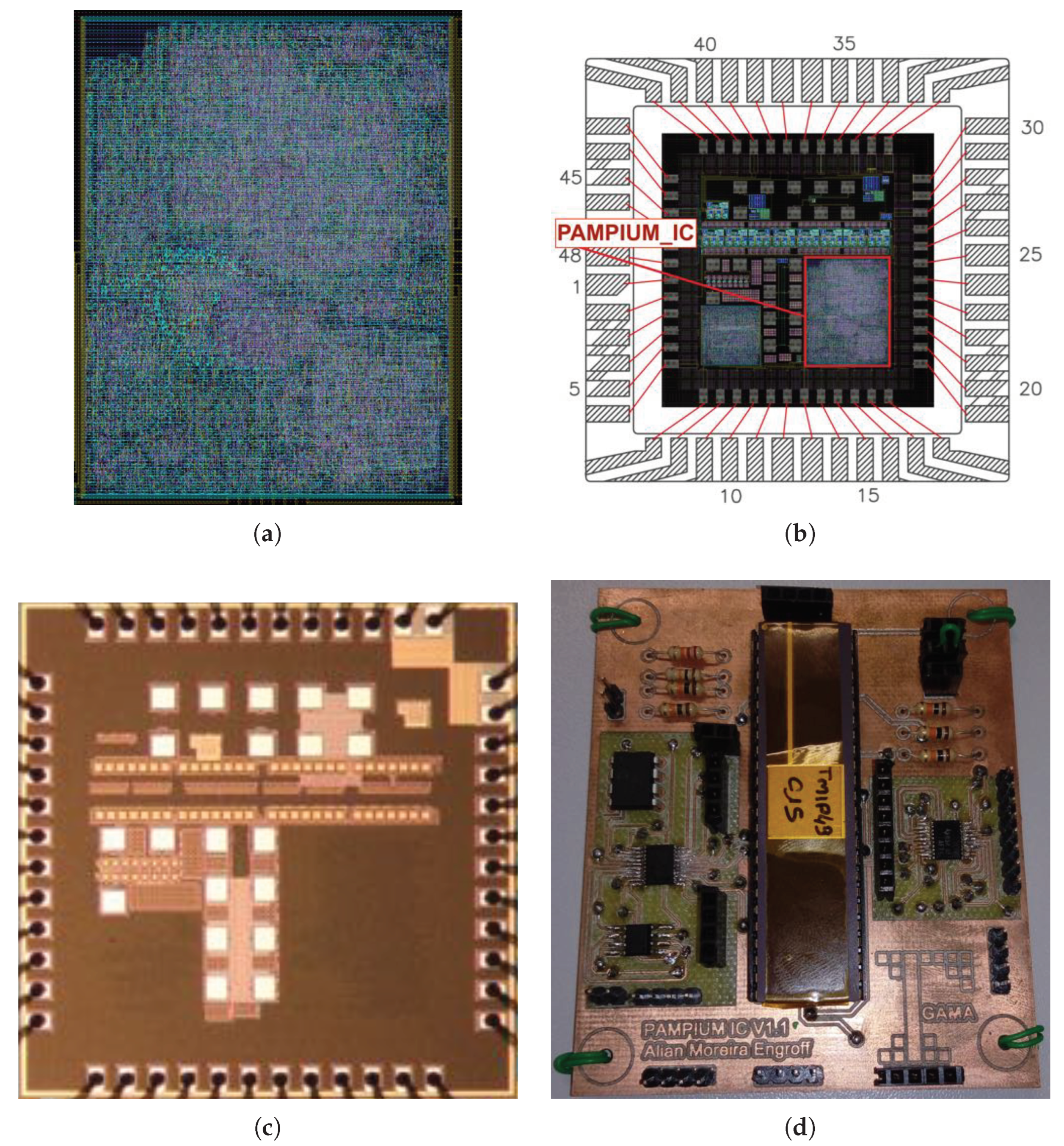
The customized ISA is composed of 21 instructions. The layout of the PAMPIUM IC obtained after the physical synthesis for 0.18 μm technology is presented in
Figure 23a.
Three clock trees were considered: program memory clock (Flash type), data memory clock (SRAM), and internal clock. Maximum delays of 10 ns, 20 ns, and 100 ns were determined for program memory, data memory, and internal clock, respectively.
The minimum clock frequency required on the physical synthesis was defined as 80 MHz. This constraint is necessary to deal with the external memory operation frequencies. The internal clock divider is configured as follows: the main memory clock is equal to the main clock, the data memory clock is two times smaller than the main clock, and the processor clock is eight times slower than the main clock. So, the cache module for data memory is fed with a clock of 40 MHz and the internal processor clock works at 10 MHz.
The results obtained by the physical synthesis are summarized in
Table 7. The maximum clock frequency achieved 102.5 MHz, with an overall power consumption of 19 mW. It meets the performance requirement. The final layout achieved an area of 500 μm × 627 μm = 0.314 mm
2, which is inside the area constraint.
The circuit was validated for the timing constraints and the communication modules were tested, as well as the instruction behavior. The final layout of the prototyped chip is shown in
Figure 23b. The PAMPIUM IC is located in the right inferior part of the chip.
The chip was prototyped by the mini@sic multi-user program from IMEC.
Figure 23c shows the microphotography of the final chip and
Figure 23d shows the test setup PCB used to extract measurement results. The measured power consumption is 28 mW for a voltage supply of 1.8 V and an operating frequency of 80 MHz. It is slightly higher than the value estimated by simulation but still meets the design power budget.
7. Conclusions
This work described the development of ASIPAMPIUM, a fast ASIP generator tool, which is suitable for the design of optimized dedicated processors. The tool provides a series of features, such as compilation, simulation, and synthesis of a C code to logic level. The generated ASIP is based on PAMPIUM architecture, which can be customized for different applications. The processor optimization in terms of low power consumption and small silicon area can be achieved by exploring instruction-level parallelism, customized ISA, and data word length.
The application of ASIPAMPIUM for generating a customized FFT ASIP shows the capabilities of the tool. The superscalar version presented the lowest normalized energy consumption compared to other implementations described in the literature. Moreover, the multicycle version presented the smallest area for the calculation of a 2048-point FFT.
The prototyping of a version of PAMPIUM in silicon demonstrated the complete design flow, from the C code program to the physical implementation. It implements a dedicated ASIP with three I2C interfaces for reading six sensors in real-time, a SPI interface for transferring data to memory, and an RS232 interface for communicating with an external device. The whole system consumes 28 mW for an operating frequency of 80 MHz.
The proposed tool, in combination with the proposed ASIP design methodology, contributes to the fast implementation of dedicated hardware suitable for mobile and IoT applications. It reduces the time-to-market and provides a simple and intuitive design flow, allowing the designer to handle different design trade-offs and objectives.
Since the current version of the ASIPAMPIUM tool is limited to single-core applications, future improvements must include the possibility to deal with adaptable ASIP-based MPSoC technologies, expanding the application range for ultra-high-performance integrated systems. Furthermore, the support for hardware accelerators will provide more alternatives to the designer in the synthesis of an optimized ASIP. The development of a custom backend for the PAMPIUM ISA for a traditional optimizing compiler (such as GCC) is also an important step toward the wide adoption of the proposed methodology.


 ,
, 


