Abstract
This paper aims to solve one of the most challenging problems in designing VLSI chips for common goods, namely an efficient incorporation of security techniques while maintaining high performances of the VLSI implementation with a reduced hardware complexity. In this case, it is very important to maintain high performance at a low hardware complexity and the overheads introduced by the security techniques should be as low as possible. This paper proposes an improved approach based on a new VLSI algorithm for including the obfuscation technique in the VLSI implementation of one important DSP algorithm used in multimedia applications. The proposed approach is based on a new VLSI algorithm that decomposes type IV DCT into six quasi-cycle convolutions and allows an efficient incorporation of the obfuscation technique. The proposed method uses a regular and modular structure called quasi-cyclic convolution and the obtained architecture is based on the architectural paradigm of systolic arrays. In this way we can obtain the advantages introduced by systolic arrays, especially high speed, with an efficient utilization of the hardware structure. Moreover, using the proposed VLSI algorithm, we can obtain the important benefit of attaining hardware security. Thus, a more efficient VLSI architecture for type IV DCT can be obtained, with a significant reduction of the hardware complexity, and an efficient incorporation of an improved hardware security mechanism with low overheads. These features are very important for resource-constrained common goods.
1. Introduction
The discrete transforms DCT-IV and DST-IV were introduced by Jain [1] and have some important applications in the area of digital signal processing as spectral analysis, signal and image coding [2,3,4] and are valid candidates to be used in data compression. DCT II, DCT III and DCT IV are computationally intensive, and in order to be used in real-time applications, it is necessary to use VLSI implementations for them. In order to obtain an efficient VLSI implementation, it is necessary to design new VLSI algorithms or to efficiently reformulate the basic form of these algorithms.
To obtain an efficient VLSI implementation, it is very important to take into consideration the data flow within the structure of the algorithm and implicitly to take into consideration the data dependencies between different operations together with its complexity and its structure, especially regularity and modularity. Using these ideas, in the present paper, we have efficiently reformulated the algorithm for DCT-IV, taking into consideration in the same time the complexity and the structure of the data flow and also its arithmetic complexity. In order to do this, we are using structures that are regular and modular, and at the same time we have significantly reduced the overall arithmetical complexity. In this paper, we have used quasi-cycle convolution structures that have some advantages from a VLSI-implementation point of view similar to those of cyclic convolution and circular correlation that have been used in the literature to obtain efficient VLSI implementations using appropriate architectural paradigms as systolic arrays architecture [5] or distributed arithmetic.
In our days, when many companies have to integrate different IP macro-cells from different supply vendors to reduce the cost of the design, it is very important to protect the designs from piracy, malicious alteration or reverse engineering. Thus, hardware security has become one of the most important topics and one of great concern.
There are several hardware security solutions, but one of the most efficient solutions for solving hardware security problems is obfuscation [6,7,8,9,10,11,12,13,14,15,16].
In the Refs. [6,8], several types of obfuscation are introduced and analyzed: the fixed obfuscation, the time-varying obfuscation and the dynamic obfuscation.
The principle for a key-based hardware security is that the protected system works correctly only when the correct key is applied and thus the design is protected by using encrypting keys for preventing any illegal access. In a mode-based obfuscation using control flow, we can exploit the properties of control flow to generate functionally incorrect modes. Thus, for the correct key, the true control signals are transmitted and for erroneous keys obfuscated false control signals will be applied. This obfuscation solution can be implemented using supplementary gates or by multiplexers. In the case of using multiplexers, as in our paper, we apply at the inputs of the multiplexer the correct and obfuscated signals, but the selection of the correct control signal is dependent on the actual key used; this means that for the correct key, the correct control signals will be selected and the correct mode will be obtained, and for a wrong key, obfuscated control signals will be selected resulting in an erroneous function.
There are several VLSI implementations for direct and inverse DCT [17,18,19,20,21,22,23,24,25,26,27], but only a few optimal VLSI implementations for type IV DCT or type IV DST [28,29,30,31,32,33,34,35,36,37,38]. Until now, there is no efficient VLSI implementation for type IV DCT or type IV DST that allows an efficient implementation of a hardware security technique, excepting our papers [31,32].
Based on the obfuscation technique introduced in [6], this paper introduces an efficient VLSI algorithm for DCT IV that allows an efficient decomposition of the DCT IV computation into six regular and modular computation structures called quasi-cycle convolutions. Moreover, the obtained VLSI algorithm has the added advantage of allowing an efficient incorporation of the hardware security.
The main contributions of this paper can be summarized as follows:
- An efficient reformulation of the DCT IV algorithm that allows a decomposition of the algorithm into only six regular and modular computation structures called quasi-cycle convolutions.
- Using the proposed VLSI algorithm, a significant reduction of the hardware complexity has been attained by using only six matrix-vector products instead of eight, as reported in the literature.
- The proposed VLSI algorithm allows a further reduction of the hardware complexity and also improves the speed performances by replacing the general multipliers with multipliers implemented using a small number of adders or subtractors.
- The proposed solution allows an efficient incorporation of the hardware security techniques with low overheads, which is important for devices produced on a large scale such as common goods.
- It allows designing of an efficient VLSI architecture with a significantly reduced hardware complexity as compared with existing solutions. It also maintains high speed performances using parallel processing and pipelining, and even improves on them.
The rest of the paper is organized as follows: Section 2 presents the new VLSI algorithm for type IV DCT with a low computational complexity using regular and modular computational structures well adapted for an efficient VLSI implementation. Section 3 presents the obtained VLSI architecture that allows a more efficient implementation of the VLSI algorithm with a significant reduction of the hardware complexity and which allows a more efficient incorporation of the obfuscation technique. Section 4 presents the obtained results. In Section 5, we discuss the results and we put in evidence for the advantages of the proposed solution. In Section 6 we present the conclusions.
2. A New VLSI Algorithm for DCT IV
The 1-D type IV DCT (DCT-IV) for a real input sequence , is defined as:
for k = 0, 1,…, N − 1
We can drop the constant coefficient from the definition of the DCT-IV, and we will add it at the end by including a multiplier at the end of the VLSI array to scale the output sequence with this constant or even better in order to increase the degree of obfuscation our IP can provide. It can be sent without this multiplier and it will be added in the final design.
In order to efficiently reformulate Equation (1) in view of obtaining an efficient VLSI algorithm, we have used some input and output restructuring sequences and we have permuted them appropriately. Thus, we can obtain a parallel decomposition of the algorithm that uses some special computation structures called quasi-cycle convolution.
The output sequence can be computed using the following equation:
for k = 1,…, N − 1
In Equation (3) we have used an auxiliary output sequence that can be computed recursively as follows:
for k = 1,…, N − 1
where we have introduced the following auxiliary input sequence:
The input auxiliary sequence is recursively computed as follows:
for i = N − 2,…, 0
The new auxiliary output sequence can be computed in parallel using six short quasi-cycle convolution structures if the transform length N is a prime number. In the following we consider the transform length N = 13.
Thus, we can compute the auxiliary output sequence using only six quasi cyclic convolutions, as will be shown below.
The first quasi-cyclic convolution is:
with:
As can be seen from Equation (9) we have a regular and modular computational structure called quasi-cyclic convolution where all the elements along the main diagonal are the same excepting the sign. The same property is true for the elements on the lines parallel with the main diagonal. In this matrix–vector product, the vector has constant elements as opposed to the case presented in [32] where these elements are variable. This property can be exploited to significantly reduce the hardware complexity of the VLSI implementation.
We have also the second quasi-cyclic convolution given by the following equation:
with:
The third quasi-cycle convolution is given by:
with:
Finally, we can compute the even part of the auxiliary output sequence T(k) combining the results of the quasi-cycle convolutions presented above as follows:
As compared with the basic equations from [32], it can be seen that the even part of the auxiliary output sequence can be computed using only three matrix–vector products instead of four having also a regular and modular structure. Moreover, the elements of the vectors in the matrix-vector products are constant as opposed with the situation presented in [32]. This property can be used to further reduce the hardware complexity as will be shown in the next sections.
The odd elements of the auxiliary output sequence can be computed as will be presented below.
Thus, we are computing the 4th quasi-cycle convolution as:
with:
and the 5th quasi-cycle convolution as follows:
with:
The 6th quasi-cycle convolution is computed as follows:
with:
Finally, we can compute the odd part of the auxiliary output sequence T(k) combining the results of the above quasi-cycle convolutions as follows:
where we have noted:
with
As compared with the basic equations used in [32], it can be seen that the odd part of the auxiliary output sequence can be computed using also only three matrix–vector products instead of four such matrix–vector products. It also has a regular and modular structure, but the elements of the vectors in such computational structures are constant as opposed to the situation presented in [32]. This property can be further used to significantly reduce the hardware complexity of the VLSI architecture that can be obtained using the proposed VLSI algorithm.
Using two auxiliary input sequences and then an appropriate recurrence given by Equations (7) and (8) and two auxiliary output sequences, we can appropriately reformulate the computation of the DCT IV algorithm using six short quasi-cycle convolution structures.
We have reordered the resulting computations using the following permutations:
where we have used the primitive root g = 2 of the Galois field formed by the transform indexes.
3. The VLSI Architecture for DCT IV Obtained Using the Proposed VLSI Algorithm
3.1. Designing the VLSI Architecture
Using the data dependence graph method [5] and the tag control mechanism [39], we have obtained six linear systolic arrays instead of eight as in [32]. The data dependence graph (DDG) has been used to put in evidence all the items involved in the proposed VLSI algorithm and the relations between them and can be used as the main instrument in our design procedure.
It can be seen from Figure 1, Figure 2, Figure 3, Figure 4, Figure 5, Figure 6 and Figure 7 that each systolic array consists of three processing elements. The linear systolic arrays implement six short quasi-cycle convolution structures having the same structure and the same length which leads to a significant hardware cost reduction as compared with similar implementations reported in the literature. Moreover, each processing element in these systolic arrays contains one multiplier with a constant instead of a general multiplier where both operands are variable. In Figure 2, Figure 3, Figure 4, Figure 5, Figure 6 and Figure 7 we are representing the delay with one clock cycle by “*”.
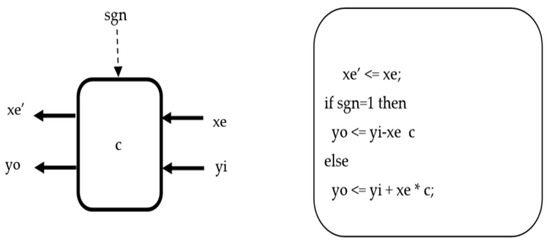

Figure 2.
Systolic array that implements Equation (9).

Figure 3.
Systolic array that implements Equation (13).
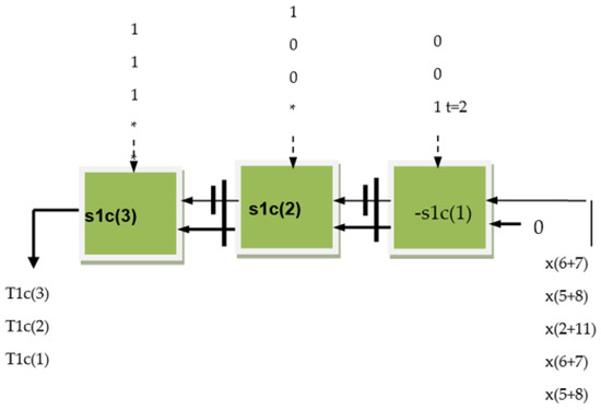
Figure 4.
Systolic array that implements Equation (17).
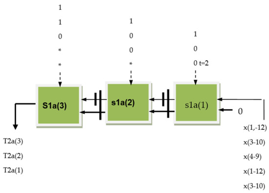
Figure 5.
Systolic array that implements Equation (22).

Figure 6.
Systolic array that implements Equation (26).
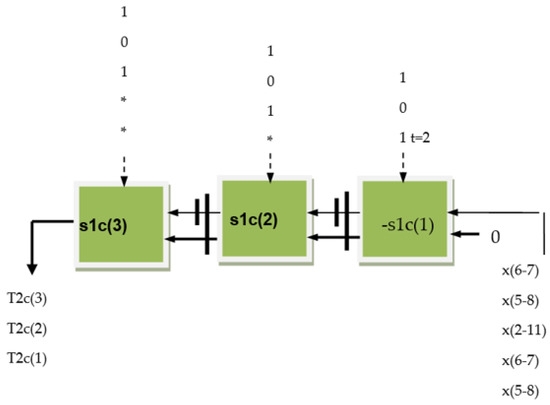
Figure 7.
Systolic array that implements Equation (30).
Due to the fact that in each multiplier one operand is constant, we can obtain an efficient implementation of these multipliers as will be presented below. It is important to note that the overall hardware complexity of a processing element is dominated by an efficient implementation of the multipliers used in each processing element.
First of all, we have represented the constant using an efficient representation in such a way that the multiplication with a constant can be implemented using adders or subtractors and shift operations as shown in Table 1.

Table 1.
Signed Digit representation of the multipliers with constants.
In Figure 8, the implementation of the multiplier having the constant operand that requires two adders and two subtracters is shown. The shifters do not involve any additional circuits but are only implemented using appropriate interconnections. In Figure 1 we have figured the cut-set lines in order to pipeline the structure. At the intersection of the cut-set lines with the arrows, we are placing pipeline registers. Thus, the critical path has been reduced from 3 × Ta to Ta where Ta represents the delay introduced by an adder or subtracter. The same structure can be used to implement multipliers with constants and that involve the same number of adders/subtracters but the shifting operations are implemented with a different constant.
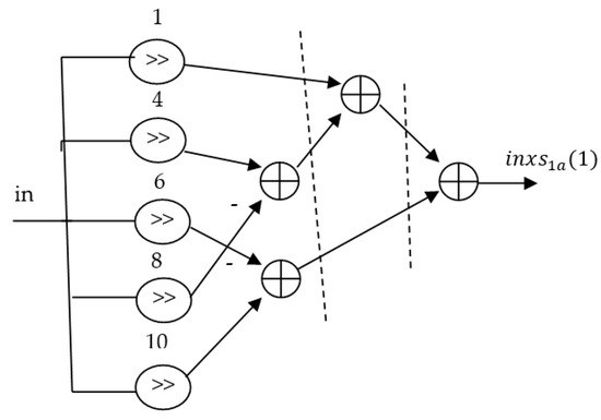
Figure 8.
The implementation of the multiplier having the constant operand .
In Figure 9, the implementation of the multiplier having the constant operand using two adders and one subtracter is shown. In this case, we are using a single cut-set line. The critical path is also Ta. The same structure is used to implement multiplications with the constants (2), s(4) and (3) but the shifting operations are implemented with different constants and the signs could be different.
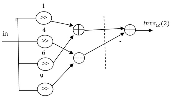
Figure 9.
The implementation of the multiplier having the constant operand s1c(2).
In Figure 10, the implementation of the multiplier having the constant operand s(1) using two subtractors is shown. In this case, we have also used a single cut-set line and the critical path will be Ta, as well. The same structure is used to implement multiplications with the constant s(3) and s(4) but the shifting operation is implemented with a different constant and the signs are different.
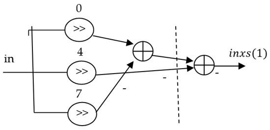
Figure 10.
The implementation of the multiplier having the constant operand s(1).
Thus, the complexity of processing elements is significantly reduced as compared with [32] due to the fact that a constant multiplier has a significantly reduced complexity as compared with a general multiplier on 12 bits. Additionally, the critical path is significantly smaller compared with the case of a general multiplier.
The function of a processing element is given in Figure 1 and is quite similar with that of a processing element from [32] but instead of a general multiplier, we have a multiplier with a constant that is more simple and which has a significantly reduced complexity. It can be seen that each processing element contains a multiplier and an adder or subtracter. The selection of the sign is done using a tag control bit denoted in Figure 1 as sgn.
3.2. The Obfuscation Technique Used in the Proposed Design
In this section, we describe the basic principle of creating obfuscation using a mode based obfuscation technique [6,15,16].
The control bits from Figure 2, Figure 3, Figure 4, Figure 5, Figure 6 and Figure 7 are used for controlling the sign of the computations. Thus, the proposed architecture has three control bits for each systolic array that are using three Pes, and the technique of obfuscation inspired by [6] can be implemented by modifying the control bits. In this way we have as a result multiple outputs with only one being the right one and the rest of them being obfuscated.
As can be seen from Figure 11, the sign bits of the systolic array from Figure 2 can be obfuscated using the sign bits sgn from the other processing elements or from the other systolic arrays. Thus, the sign bits of the first processing element from Figure 2 denoted in Figure 11 as sgn (1,1) can be applied to the first processing element from Figure 2 only when the key bits K[0:1] are 01. In the other cases, the sign bits that are applied for the first processing element from the systolic array from Figure 2 will be the sign bits for processing element two from the systolic array from Figure 3 sgn(2,1) or the sign bits from the third element from the systolic array from Figure 4 sgn(3,1) or the sign bits from the second processing element from the first systolic array from Figure 2 sgn(1,2). The same ideas are used for the sign bits of the second processing element of the systolic array from Figure 5 “s2”. Only when the key bits K[2:3] are 10, the correct sign bits sgn(1,2) are applied for the second processing element from Figure 5. For the other values of the key bits K[2:3], the sign bits s2 applied for the second processing element of the systolic array from Figure 2 will be the sign bits sgn(1,1) from the first processing element of the first systolic array from Figure 2 or the sign bits sgn(3,2) from the second processing element from Figure 4 or the sign bits sgn(4,3) from the third element of the systolic array from Figure 5. Additionally, for the obfuscated sign bits s3 of the third element of the systolic array from Figure 2, only when the key bits K[4:3] are 01 we have the correct sign bits for this processing element. For the other values of these key bits we are applying the wrong sign bits sgn(2,3) from the third processing element of the systolic array from Figure 3 or the sign bits sgn(3,2) from the second processing element from the systolic array from Figure 4 or the sign bits sgn(4,2) from the second processing element of the systolic array from Figure 5.
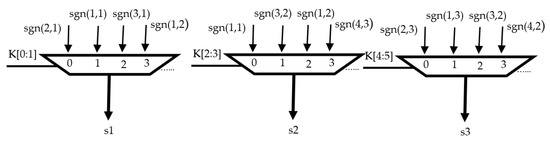
Figure 11.
The principle of the implementation of the proposed obfuscation technique.
The right sign bits s1–s3 for the processing elements from the systolic array from Figure 2 are obtained when the key bits K[0:5] are 011001, while for the other combinations, erroneous sign bits are selected using the MUXs from Figure 11 and thus erroneous results are obtained. The combination formed by K[0:5] represents the obfuscation key.
The same ideas are used to obfuscate the sign bits for the processing elements of the systolic arrays from Figure 3, Figure 4, Figure 5, Figure 6 and Figure 7.
The right sign bits s1–s3 are obtained when K[0:1] = 01, K[1] = 0, K[2:3] = 10 and K[3:4] = 01, while for the other values, erroneous control signals are selected. The combination formed by K[0:5], represents the obfuscation key for the first systolic array.
The proposed obfuscation scheme is simple and involves low overheads, which is very important for common goods that are in mass production. We are using only one MUX with four inputs on one bit and one output on one bit for each processing element from Figure 2, Figure 3, Figure 4, Figure 5, Figure 6 and Figure 7. Additionally, all the signals used in obfuscation are similar and the signal used in obfuscation represents the correct sign bits but for other processing elements from the VLSI architecture.
This increases the degree of confusion and implicitly of obfuscation. This could be very useful in the case where reverse engineering is used to discover the correct signals.
3.3. The VLSI Architecture for the Hardware Core of the VLSI Implementation of DCT IV
Using a hardware sharing technique, we can combine the systolic arrays from Figure 2 and Figure 5 and obtain the unified systolic array from Figure 12. We are also combining the obfuscation circuits for the two systolic arrays. It can be seen that the same multiplier is used in each processing element for the two systolic arrays from Figure 2 and Figure 5.
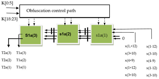
Figure 12.
Systolic array that implement Equations (9) and (22).
Using the same hardware sharing technique, we can also combine the systolic arrays from Figure 3 and Figure 6 and obtain the unified systolic array from Figure 13. It can be seen also that the same multiplier is used in each processing element for the two systolic arrays from Figure 3 and Figure 6.
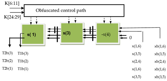
Figure 13.
Systolic array that implements Equations (13) and (26).
The same hardware sharing technique is also used to combine the systolic arrays from Figure 4 and Figure 7, and we obtain the unified systolic array from Figure 14. It can be seen also that the same multiplier is used in each processing element for the two systolic arrays.
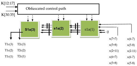
Figure 14.
Systolic array that implements Equations (17) and (30).
In addition to the hardware core that consists of the systolic arrays from Figure 12, Figure 13 and Figure 14, we have a pre-processing and a post-processing stage. The pre-processing stage computes the auxiliary input sequences xa(i,j) and xb(i,j) and performs the index mapping given by Equations (39) and (40) and implements relations (6–8) and (14–16) and (27–29) that involves mainly addition and one multiplication. The post-processing stage is used to compute the auxiliary output sequence T(k) using Equations (21) and (34), the auxiliary output sequence Ta(k) using the recurrences given by (4) and (5) and finally, the output sequence using Equation (3). Only in the final Equation (3) we have one multiplier in rest only additions/subtractions.
4. Results
As has been shown in Section 3, using the obtained VLSI algorithm for type IV DCT, it was possible to use a more efficient obfuscation technique as in [32] with only a slight increase of the overheads. The overhead involved by the incorporation of the obfuscation technique is very low and consists only in 18 MUXs on one bit with 4 inputs and one output.
Additionally, a significant reduction of the hardware complexity as compared with the best VLSI implementation of the DCT IV [32] could be obtained maintaining in the same time the same speed performances. Thus, using the proposed VLSI algorithm, we have obtained a new VLSI architecture with only three linear systolic arrays elements working in parallel, containing each three processing elements, instead of eight such systolic arrays as in the best solution presented in the literature [32]. Moreover, due to the fact that each processing element contains two multipliers with the same constant, we can apply a hardware sharing technique, and instead of two such multipliers, we can use only one in each processing element. The complexity of the multipliers has been also reduced significantly due to the fact that the multiplication with a constant can be implemented using only a few adders and subtracters as has been shown in Section 3. Thus, the complexity of the multipliers has been significantly reduced as compared with that of a general multiplier used in [32] and we can use in our VLSI architecture of the hardware core only adders and subtracters and shift operations that can be implemented without extra circuits.
5. Discussion
We have obtained a new VLSI algorithm for type IV DCT that allows using a more efficient obfuscation technique compared with that proposed in [32] with only a slight increase of the overheads. In the same time a significant reduction of the hardware complexity has been obtained. For the proposed VLSI algorithm we have obtained a new VLSI architecture with only 3 linear systolic arrays working in parallel, containing each 3 processing elements, instead of 8 such systolic arrays as in the best solution presented in the literature [32]. Due to the fact that each processing element contains 2 multipliers with the same constant, we can apply a hardware sharing technique and instead of 2 such multipliers we can use only one in each processing element. Moreover, the complexity of the multipliers with a constant can be significantly reduced as compared with the general multiplier used in [32]. Thus, we can use only adders and subtracters and shift operations, as can be seen from the Table 1, to implement the constant multipliers.
5.1. Discussion about the Main Futures of the Proposed Solution
As shown in Section 3.2, the hardware security has been increased and the overhead involved by the incorporation of the obfuscation technique is very low and consists only in 18 MUXs on one bit with four inputs and one output.
We are using only 6 regular and modular computation structures (a matrix–vector product) where all the elements of the vectors are constant. This feature can be further exploited by replacing the general multipliers with only a few adders and subtracters leading to a further reduction of the hardware complexity and in the same time a reduction of the critical path and an increase of the speed performances.
The proposed VLSI algorithm can be mapped on six linear systolic arrays that can be merged in only three such systolic arrays.
Due to the fact that three systolic arrays have multipliers with the same constants, we can further reduce the hardware complexity by applying a hardware-sharing technique, and instead of two such multipliers, we can use only one in each processing element. The proposed VLSI algorithm can be mapped thus on only three linear systolic arrays with a significant reduction of the hardware complexity.
5.2. Comparison with Similar Solutions for the VLSI Implementation of DCT IV
As can be seen from Table 2, in [34] the throughput is two times lower as compared with our solution where we have six systolic arrays working in parallel as compared with two systolic arrays used in [34]. Moreover, the solution proposed in [28,34] does not incorporate the obfuscation technique.
Table 2.
Comparison of the hardware complexity and speed performances of various DCT IV designs.
As can be seen from Table 2 comparing with [32] (the best reported in the literature), we have significantly reduced the number of multipliers and adders due to the fact that we have three systolic arrays with three processing elements instead of four systolic arrays with three processing elements as in [32]. The complexity of a processing element in the two solutions is similar. Moreover, due to the fact that we are using only multipliers with a constant operand, we can implement these multipliers at a low cost using at most four adders/subtractors to implement a such multiplier instead having a general multiplier as in [32] with a complexity that is significantly greater. Moreover, the general multiplier is significantly slower.
Thus, we have nine (3(N − 1)/4 in general case) multipliers with a constant that can be implemented using only 28 adders/subtracters with a critical path of of Ta, where Ta is the latency of an adder instead of 12 ((N − 1)) general multipliers with the critical path of Ta + Tm where Tm is the latency of a general multiplier on 12 bits that is significantly greater than that of an adder Ta.
In [28] we have the same number of multipliers for the hardware core as in [32] and the critical path is also Ta + Tm.
Thus, we can obtain better speed performances as in [28,31,32] due to the fact that the clock frequency is given by the critical path that is significantly better in our design As compared with [34] the throughput is doubled. Thus, we have high speed processing, using a parallel decomposition of the VLSI algorithm and greater than in [32], taking into consideration the reduction of the critical path, and obtaining in the same time a significant reduction of the hardware complexity as have been shown above. The proposed solution has also all the advantages of a VLSI implementation of cycle convolution or circular correlation as a good topology that allows an efficient VLSI implementation and a low I/O cost.
6. Conclusions
In this paper, a new solution to obtain an efficient VLSI implementation for DCT IV with a significant reduction of the hardware complexity has been proposed. In the same time, an efficient hardware security technique with very low overheads, that is very important for resource-constrained common goods, has been incorporated. The proposed solution is based on a new efficient VLSI algorithm for DCT IV that decomposes the computation of DCT IV into six quasi-cycle convolutions instead of eight such computational structures as reported into literature. The proposed VLSI architecture is inspired by the architectural paradigm of systolic arrays, thus obtaining the advantages introduced by the VLSI implementation of such regular and modular structures using systolic arrays as high speed and an efficient utilization of the hardware structure with low I/O costs. Moreover, the proposed solution has the added benefit of efficiently attaining hardware security. Thus, we have obtained the benefit of attaining hardware security using very low overheads and obtaining at the same time a very efficient VLSI implementation with a significant reduction of the hardware complexity and high-speed performances.
Funding
This work was supported by a grant of the Romanian Ministry of Education and Research, CNCS—UEFISCDI, project number PCE 172/2020 (PN-III-P4-ID-PCE2020-0713), within PNCDI III.
Institutional Review Board Statement
Not applicable.
Informed Consent Statement
Not applicable.
Data Availability Statement
Not applicable.
Acknowledgments
The author would like to thank the Romanian Ministry of Education and Research for their support in offering the grant CNCS—UEFISCDI, project number PCE 172 (PN-III-P4-ID-PCE2020-0713, within PNCDI III).
Conflicts of Interest
The authors declare no conflict of interest.
References
- Jain, A.K. A sinosoidal family of unitary transforms. IEEE Trans. Pattern Mach. Intell. 1979, I, 356–365. [Google Scholar] [CrossRef] [PubMed]
- Jing, C.; Tai, H.-M. Fast algorithm for computing modulated lapped transform. Electron. Lett. 2001, 37, 796–797. [Google Scholar] [CrossRef]
- Malvar, H.S. Lapped transforms for efficient transforms/subband coding. IEEE Trans. Acoust. Speech Signal Process. 1990, 38, 969–978. [Google Scholar] [CrossRef]
- Malvar, H.S. Signal Processing with Lapped Transforms; Artech House: Norwood, MA, USA, 1991. [Google Scholar]
- Kung, S.Y. VLSI Array Processors; Prentice Hall: Englewood Cliffs, NJ, USA, 1988. [Google Scholar]
- Koteshwara, S.; Kim, C.H.; Parhi, K.K. Key-Based Dynamic Functional Obfuscation of Integrated Circuits using Sequentially-Triggered Mode-Based Design. IEEE Trans. Inf. Forensics Secur. 2018, 13, 79–93. [Google Scholar] [CrossRef]
- Chakraborty, R.S.; Bhunia, S. Security against hardware Trojan through a novel application of design obfuscation. In Proceedings of the 2009 IEEE/ACM International Conference on Computer-Aided Design-Digest of Technical Papers, San Jose, CA, USA, 2–5 November 2009; pp. 113–116. [Google Scholar]
- Knechtel, J.; Patnaik, S.; Sinanoglu, O. Protect your chip design intellectual property: An overview. In Proceedings of the International Conference on Omni-Layer Intelligent Systems, Barcelona, Spain, 1–3 August 2019; pp. 211–216. [Google Scholar]
- Pilato, C.; Garg, S.; Wu, K.; Karri, R.; Regazzoni, F. Securing hardware accelerators: A new challenge for high-level synthesis. IEEE Embedded Syst. Lett. 2018, 10, 77–80. [Google Scholar] [CrossRef]
- Zhang, J. A practical logic obfuscation technique for hardware security. IEEE Trans. Very Large Scale Integr. (VLSI) Syst. 2016, 24, 1193–1197. [Google Scholar] [CrossRef]
- Chen, S.; Chen, J.; Wang, L. A chip-level anti-reverse engineering technique. J. Emerg. Technol. Comput. Syst. 2018, 2, 1–20. [Google Scholar] [CrossRef]
- Shamsi, K.; Li, M.; Meade, T.; Zhao, Z.; Pan, D.Z.; Jin, Y. AppSAT: Approximately deobfuscating integrated circuits. In Proceedings of the 2017 IEEE International Symposium on Hardware Oriented Security and Trust (HOST), Mclean, VA, USA, 1–5 May 2017; pp. 95–100. [Google Scholar]
- Sengupta, A.; Roy, D.; Mohanty, S.P.; Corcoran, P. Low-cost obfuscated JPEG CODEC IP core for secure CE hardware. IEEE Trans. Consum. Electron. 2018, 64, 365–374. [Google Scholar] [CrossRef]
- Sengupta, A.; Roy, D.; Mohanty, S.P.; Corcoran, P. DSP design protection in CE through algorithmic transformation based structural obfuscation. IEEE Trans. Consum. Electron. 2017, 63, 467–476. [Google Scholar] [CrossRef]
- Parhi, K.K.; Koteshwara, S. Dynamic Functional Obfuscation. U.S. Patent 15/667 776, 3 August 2017. [Google Scholar]
- Koteshwara, S.; Kim, C.H.; Parhi, K.K. Hierarchical functional obfuscation of integrated circuits using a mode-based approach. In Proceedings of the 2017 IEEE International Symposium on Circuits and Systems (ISCAS), Baltimore, MD, USA, 28–31 May 2017. [Google Scholar]
- Chiper, D.F.; Cotorobai, L. A Unified VLSI architecture for 1D IDCT and IDST based on pseudo-band correlations. In Proceedings of the 10th International Conference on Electronics, Computers and Artificial Intelligence (ECAI), Iasi, Romania, 28–30 June 2018. [Google Scholar]
- Xie, J.; Meher, P.K.; He, J. Hardware-Efficient Realization of Prime-Length DCT Based on Distributed Arithmetic. IEEE Trans. Comput. 2013, 62, 1170–1178. [Google Scholar] [CrossRef]
- Chen, Z.; Han, Q.; Cham, W.-K. Low-Complexity Order-64 Integer Cosine Transform Design and Its Application in HEVC. IEEE Trans. Circuits Syst. Video Technol. 2018, 28, 2407–2412. [Google Scholar] [CrossRef]
- Meher, P.K. Systolic designs for DCT using low-complexity concurrent convolutional formulation. IEEE Trans. Circuits Syst. Video Technol. 2006, 16, 1041–1050. [Google Scholar] [CrossRef]
- Chiper, D.F. A new systolic array algorithm for memory-based VLSI array implementation of DCT. In Proceedings of the Proceedings Second IEEE Symposium on Computer and Communications, Alexandria, Egypt, 1–3 July 1997; pp. 297–301. [Google Scholar]
- Yu, S.; Swartzlander, E.E. DCT Implementation with Distributed Arithmetic. IEEE Trans. Comput. 2001, 50, 985–991. [Google Scholar]
- Kim, D.W.; Kwon, T.W.; Seo, J.M.; Yu, J.K.; Lee, S.K.; Suk, J.H.; Choi, J.R. A compatible DCT/IDCT architecture using hardwired distributed arithmetic. In Proceedings of the ISCAS 2001. The 2001 IEEE International Symposium on Circuits and Systems ISCAS’2001, Sydney, NSW, Australia, 6–9 May 2001; Volume II, pp. 457–460. [Google Scholar]
- Madisetti, A.; Wilson, A.N., Jr. A 100 Mhz 2-D 8x8 DCT/IDCT processor for HDTV applications. IEEE Trans. Circuits Syst. Video Technol. 1995, 5, 158–165. [Google Scholar] [CrossRef]
- Chiper, D.F.; Swamy, M.N.S.; Ahmad, M.O. An Efficient Unified Framework for the VLSI Implementation of a Prime-Length DCT/IDCT with High Throughput. IEEE Trans. Signal Process. 2007, 54, 2925–2936. [Google Scholar] [CrossRef]
- Hsiao, S.F.; Shiue, W.R.; Tseng, J.M. Design and implementation of a novel linear array DCT/IDCT processor with complexity of order. IEEE Proc. Vis. Image Signal Process. 2000, 147, 400–408. [Google Scholar] [CrossRef]
- Chiper, D.F.; Ungureanu, P. Novel VLSI Algorithm and Architecture with Good Quantization Properties for a High-Throughput Area Efficient Systolic Array Implementation of DCT. EURASIP J. Adv. Signal Process. 2011, 2011, 1–14. [Google Scholar] [CrossRef]
- Chiper, D.F. New VLSI Algortihm for a High-Throughput Implementation of Type IV DCT. In Proceedings of the International Conference on Communications (COMM), Bucharest, Romania, 9–11 June 2016. [Google Scholar]
- Luo, C.; Ma, W.; Juang, W.; Kuo, S.; Chen, C.; Tai, P.; Lai, S. An ECG Acquisition System Prototype Design with Flexible PDMS Dry Electrodes and Variable Transform Length DCT-IV Based Compression Algorithm. IEEE Sens. J. 2016, 16, 8244–8254. [Google Scholar] [CrossRef]
- Lai, S.-C.; Chien, W.-C.; Lan, C.-S.; Lee, M.-K.; Luo, C.-H.; Lei, S.-F. An efficient DCT-IV-based ECG compression algorithm and its hardware accelerator design. In Proceedings of the International Symposium on Circuits and Systems (ISCAS), Daegu, Republic of Korea, 19–23 March 2013; pp. 1296–1299. [Google Scholar]
- Chiper, D.F.; Cotorobai, L. A New VLSI Algorithm for type IV DCT for an Efficient Implementation of Obfuscation Technique. In Proceedings of the 43rd International Conference on Telecommunications and Signal Processing (TSP), Milan, Italy, 7–9 July 2020. [Google Scholar]
- Chiper, D.F.; Cotorobai, L.T. A New Approach for a Unified Architecture for Type IV DCT/DST with an Efficient Incorporation of Obfuscation Technique. Electronics 2021, 10, 1656. [Google Scholar] [CrossRef]
- Chiper, D.F. A parallel VLSI algorithm for a high throughput systolic, array VLSI implementation of type IV DCT. In Proceedings of the 2009 International Symposium on Signals, Circuits and Systems, Iasi, Romania, 9–10 July 2009; Volume 1, pp. 257–260. [Google Scholar]
- Chiper, D.F. An Efficient Algorithm for a Memory-Based Systolic Array VLSI Implementation of Type IV DCT. In Proceedings of the 2015 International Symposium on Signals, Circuits and Systems (ISSCS), Iasi, Romania, 9–10 July 2015; pp. 1–4. [Google Scholar]
- Kidamni, S.S. Recursive Implementation of the DCT-IV and DST-IV. In Proceedings of the IEEE Symposium on Advances in Digital Filtering and Signal Processing. Symposium Proceedings(Cat. No.98EX185), Victoria, BC, Canada, 5–6 June 1998. [Google Scholar]
- Chiper, D.F.; Cotorobai, L. A New VLSI Algorithm for an Efficient VLSI Implementation of Type IV DST based on Short Band-Correlation Structures. In Proceedings of the 2020 13th International Conference on Communications (COMM), Bucharest, Romania, 18–20 June 2020. [Google Scholar]
- Murphy, N.R.; Swamy, M.N.S. On the On-Line Computation of DCT-IV and DST-IV Transforms. IEEE Trans. Signal Process. 1995, 43, 1249–1251. [Google Scholar] [CrossRef]
- Chiper, D.F.; Ahmad, M.O.; Swamy, M.N. A Unified VLSI Algorithm for a High Performance Systolic Array Implementation of Type IV DCT/DST. In Proceedings of the International Symposium on Signals, Circuits and Systems ISSCS, Iasi, Romania, 11–12 July 2013. [Google Scholar]
- Jen, C.W.; Hsu, H.Y. The design of a systolic array with tags input. In Proceedings of the 1988 IEEE International Symposium on Circuits and Systems (ISCAS), Espoo, Finland, 7–9 June 1988; pp. 2263–2266. [Google Scholar]
Disclaimer/Publisher’s Note: The statements, opinions and data contained in all publications are solely those of the individual author(s) and contributor(s) and not of MDPI and/or the editor(s). MDPI and/or the editor(s) disclaim responsibility for any injury to people or property resulting from any ideas, methods, instructions or products referred to in the content. |
© 2023 by the author. Licensee MDPI, Basel, Switzerland. This article is an open access article distributed under the terms and conditions of the Creative Commons Attribution (CC BY) license (https://creativecommons.org/licenses/by/4.0/).