Article

Power/Area-Efficient ECC Processor Implementation for Resource-Constrained Devices

1
Department of Electrical Engineering, College of Engineering in Wadi Alddawasir, Prince Sattam Bin Abdulaziz University, Wadi Alddawasir 11991, Saudi Arabia
2
Electronics and Micro-Electronics Laboratory, Faculty of Sciences, University of Monastir, Monastir 5000, Tunisia
3
Department of Computer Science, University College of Tayma, University of Tabuk, Tabuk 71491, Saudi Arabia
*
Author to whom correspondence should be addressed.
Electronics 2023, 12(19), 4110; https://doi.org/10.3390/electronics12194110
Submission received: 4 September 2023 / Revised: 24 September 2023 / Accepted: 27 September 2023 / Published: 30 September 2023

Abstract

:
The use of resource-constrained devices is rising nowadays, and these devices mostly operate with sensitive data. Consequently, security is a key issue for these devices. In this paper, we propose a compact ECC (elliptic curve cryptography) architecture for resource-constrained devices based on López–Dahab (LD) projective point arithmetic operations on GF(2m). To achieve an efficient area-power hardware ECC implementation, an efficient digit-serial multiplier is developed. The proposed multiplier is built on a Bivariate Polynomial Basis representation and a modified Radix-n Interleaved Multiplication (mRnIM) method (for area and power complexities reduction). Furthermore, the LD-Montgomery point multiplication algorithm is adjusted for accurate scheduling in the compact ECC architecture to eliminate data reliance and improve signal management. Meanwhile, the area complexity is reduced by reuse of resources, and clock gating and asynchronous counter are exploited to reduce the power consumption. Finally, the proposed compact ECC architecture is implemented over GF(2m) (m = 163, 233, 283, 409, and 571) on Xilinx FPGAs’ (Field-Programmable Gate Array) Virtex 5, Virtex 6, and Virtex 7, showing that the efficiency of this design outperforms to date when compared to reported works individually. It utilizes less area and consumes low power. The FPGA results clearly demonstrate that the proposed ECC architecture is appropriate for constraint-resources devices.

1. Introduction

The number of IoT (Internet of Things) hardware boards has increased considerably in recent years as a result of advancements in System-on-Chip (SoC) technology in terms of energy consumption and processing capacity, allowing them to deliver computer-like capabilities. Nonetheless, most IoT nodes include small computing devices capable of performing specialized functions as well as network communications through the Internet. These devices like cell phones, personal digital assistants (PDAs), embedded systems, sensors, and smart cards have all played an important role in human life and have become an inseparable part of the contemporary world. As these devices have severely restricted processing power, memory, and battery life resources, they may be exposed to a wide range of security threats and breaches. Furthermore, when dealing with sensitive data, the integrity of the services and the dependability of the technology they supply become a rising worry. Since the security vulnerability has not been properly rectified, such devices are vulnerable to cyber threats. Traditional public key encryption has long been seen as inadequate due to the substantial overhead it imposes on resource-constrained devices [1]. Nonetheless, ECC has lately been used in many applications due to its various benefits over traditional public key encryption systems [2]. The fact that ECC delivers a very high level of security while using fewer resources has drawn the attention of the scientific community [3,4]. As a result, ECC is currently used in a variety of security services, including key exchange, authentication, and digital signature [5,6]. To implement ECC, prime fields G F Z p can be used [7,8] or binary fields G F ( 2 m ) . The use of G F 2 m or G F Z p fields as the basis of the ECC system is based on the desired performance. The G F ( 2 m ) -based processor outperforms G F Z p in terms of area, latency, and power consumption [9]. There are many available algorithms for the point multiplication, but the most used the Montgomery Algorithm where the point doubling (PD) and point addition (PA) are executed separately.

1.1. Existing Works

Many efforts have been made to achieve an efficient hardware ECC implementation. These works can be broken down into two broad categories: system-level and component level which are explained below.
  • System-level relates mostly to the ECC system’s implementation. Some significant ECC hardware implementation are provided below.
In 2013, Sutter et al. presented an architecture for EC scalar point multiplication that is appropriate for applications that may require a speed–area trade-off [10]. They reorganized and reordered the critical path of the multiplication and division operations in order to examine the resulting performance and discover the optimal digit size. In 2015, Khan et al. presented a combined Montgomery point multiplication (MPM) algorithm to accomplish low-latency ECC point multiplication through the use of novel pipelined full- precision parallel multipliers over GF(2m) [11]. They used careful point operation scheduling and clever pipelining in the ECC design to decrease the latency by eliminating MPM data dependencies.
In 2016, Li et al. developed a Montgomery ladder method-based high-performance hardware implementation architecture for EC scalar multiplication over binary fields using polynomial basis for Finite Field (FF) arithmetic [12]. The suggested architecture employed a single Karatsuba multiplier with no idle cycle to improve FF multiplication speed while using little hardware resources, while other FF operations were executed in parallel. In the same year, the authors of [13] presented a Montgomery ladder scalar multiplication for binary elliptic curve cryptography. An efficient Itoh–Tsujii algorithm-based field inversion architecture and 3-pipelined digit-serial multipliers were used. In 2017, Khan et al. developed a modified López–Dahab MPM technique with careful scheduling to reduce data dependence in [14]. They also introduced a new pipelined bit-parallel multiplier to minimize latency. Two-stage pipelined full-precision multipliers in high-performance ECC (HPECC) and one-stage multipliers in low-latency ECC (LLECC) designs with careful scheduling are introduced.
In 2019, Imran et al. [15] presented a pipelined system to speed up elliptic curve cryptography point multiplication. This is accomplished by: pipelining the arithmetic unit which initially reduces critical path delay. Second, by carefully timing PA–PD operations to save clock cycles. In the same year, Harb et al. proposed a small elliptic curve crypto-graphic core over GF(2m) for limited-resource embedded applications [16]. The ROM-based state machine-based iterative architecture executed the design. In 2022, the authors in [17] developed an efficient large field-size ECC processor hardware implementation. They suggested an MPM technique to enhance resource consumption efficiency and ECC processor signal flow. In 2023, Nadikuda et al. developed a modified Montgomery ladder technique to decrease point multiplication clock cycles [18]. By shifting, reducing, and using NAND gates to compute the partial products, an oriented area/latency digit-serial multiplier was produced. In the same year, Amer et al. [19] developed a new hardware architecture for a compact ECC crypto processor GF(2233). An iterative bit–serial GF(2m) multiplier performed polynomial coefficient multiplication, modular squares, and inversion operations.
More recently, Rashid et al. suggested an efficient area-optimized ECC architecture for large fields [20]. With 4-split polynomials, the authors presented a hybrid Karatsuba multiplier. General Karatsuba and schoolbook multiplication methods are used in the multiplier. Finally, the authors in [21] proposes an FPGA-based area/speed-efficient ECC processor. The authors suggested an efficient digit-serial multiplier with careful Montgomery PM algorithm management for large fields. The k-way overlap-free Karatsuba algorithm and RnIM are used to build the suggested multiplier.
  • Component-level.
In light of the preceding discussion, the primary implementation of an efficient point multiplication relies on a rigorous examination of FF arithmetic operations: FF squaring, FF addition, FF multiplication, and FF inversion. Thus, in G F 2 m , polynomial addition can be implemented by bitwise XORing. However, the most time-sensitive and resource-intensive FF operations are FF multiplication and FF inversion. FF multiplication may be used to perform the FF inversion, therefore the performance of the ECC processor design is strongly related to an efficient modular multiplication structure. Many works used digit-serial FF multipliers to improve area and delay complexity. The most relevant are presented in [22,23,24,25,26]. Pipelining stages are commonly used to boost clock frequency at the price of a few more clock cycles and area overheads; these works utilized either big-size or parallel multipliers at the penalty of higher area complexity. Furthermore, if the instructions have data dependencies, the multiplier pipelining steps will cause idle cycles at the PM level. Therefore, in order to get the most out of pipelining, careful scheduling is essential.

1.2. Research Gap

In daily life, resource-constrained devices, such as wireless sensor nodes, are widely used. Several cryptographic techniques have been investigated to ensure the security of such devices, including ECC. In today’s cyber-physical world, ECC has gained enormous popularity as an important method of implementing asymmetric encryption. Due to the limited memory and power budget of embedded devices, it is necessary to develop special systems and algorithms for ECC on desired hardware architectures and platforms. However, several architectural methods have been used to improve the efficiency of ECC, including pipeline, parallelism, and many types of GF(2m) multipliers (bit-parallel, digit-parallel, digit-serial, etc.). Nevertheless, most of these designs are not suitable for resource-constrained devices due to the greater area complexity they introduce (most implementations focus on speed). Facing this challenge, in this paper, we propose an efficient area-power ECC implementation over GF(2m) (m = 163, 233, 283, 409, and 571).

1.3. Main Contributions

This paper’s significant contributions are listed below:
  • An efficient GF(2m) digit-serial multiplier based on Bivariate Polynomial Basis representation and mRnIM to reduce booth area and power.
  • An efficient ECC architecture based on a multiplier targeting the resource-constrained devices.
  • FF operations are built in parallel with the FF multiplier by rearrangement and restructuring of the López–Dahab algorithm.
  • An optimized MPM algorithm is used to minimize unnecessary latency/area use.
  • Asynchronous counters and clock gating are used to minimize power consumption.
  • Xilinx ISE timing closure techniques are used to achieve the best possible high-performance results. The experimental results using FPGA (virtex 7) show the efficiency is about 31%, 18%, 10%, 8%, and 3% compared to the best previous work using GF(2163), GF(2233), GF(2283), GF(2409), and GF(2571), respectively. This has been achieved while the area usage is about 27.43%, 58.47%, and 9.52% less than the best previous work using GF(2163), GF(2283), and GF(2409), respectively.
  • Finally, our design used a time-invariant method for each module—including Fermat’s little theorem for field inversion—to complete the point multiplication in constant time, providing security against side-channel attacks.

1.4. Organization

This article is structured as follows. Section 2 presents the background of ECC and associated arithmetic operations over GF(2m). Our proposed digit-serial GF(2m) multiplier is presented in Section 3. Section 4 presents the suggested hardware processor architecture for elliptic curves over binary fields. Section 4 also discusses the planned scheduling and other relevant improvements. Section 5 presents a thorough performance study and comparison of the proposed structure with the respective ECC implementations. Finally, Section 6 summarizes the important points and emphasizes the value of the research.

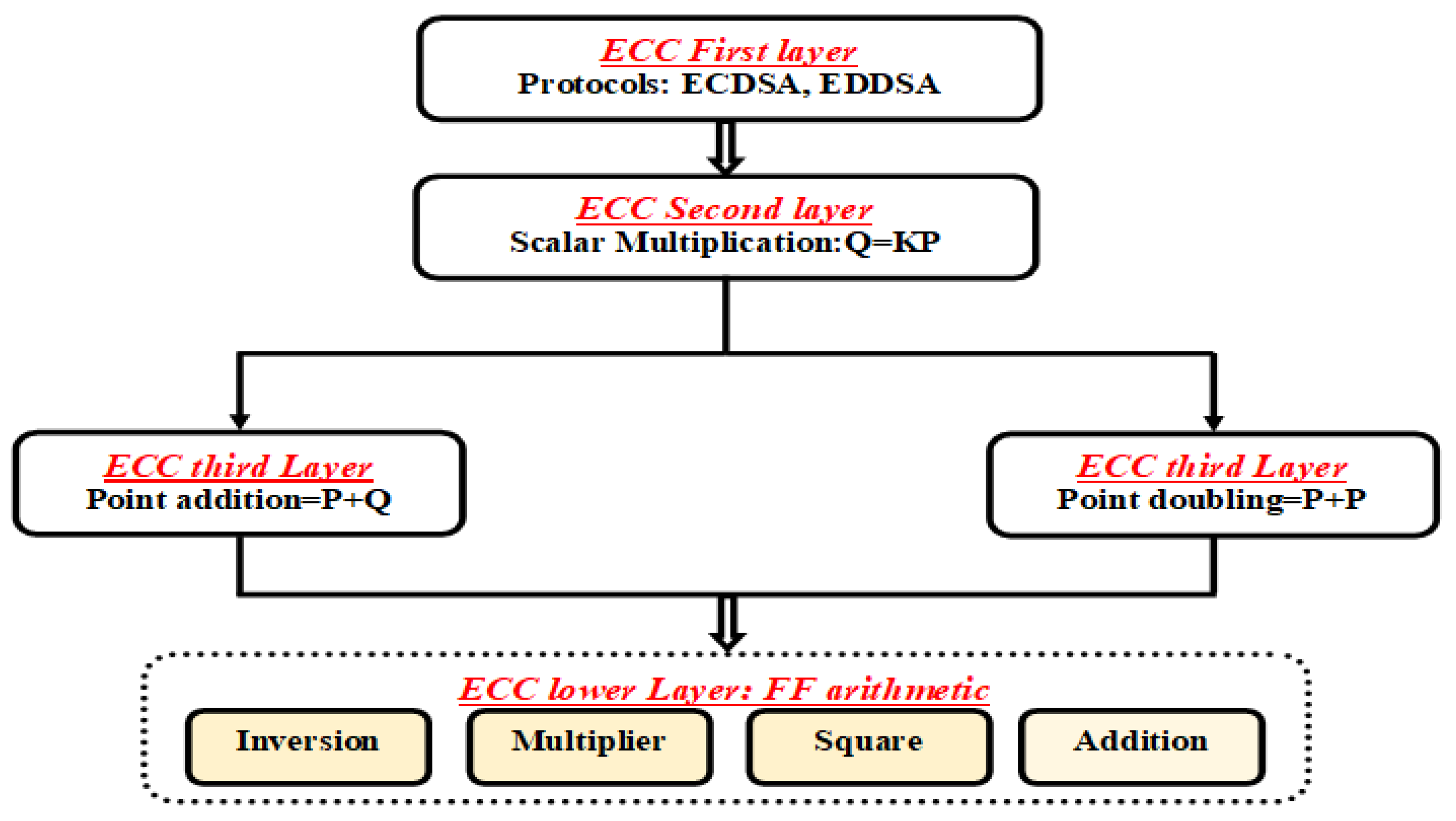
2. ECC over GF(2m) Background

A non-super singular elliptic curve equation is defined in the field GF(2m) with characteristic 2 as [24]:
E : y 2 + x y = x 3 + a x 2 + b
with a , b , x , y G F 2 m , b 0 .
Given a base point P on the curve, and a positive integer k, computing Q = KP is called scalar multiplication. The result Q is another point on the elliptic curve. The implementation hierarchy of the ECC system over the binary field GF(2m) is presented in Figure 1.
From Figure 1, scalar multiplication and ECC group operations, for example, PA and PD, are the buildings blocks of elliptic curve cryptographic schemes such as ECDSA (Elliptic Curve Digital Signature Algorithm) and ECDH (Elliptic Curve Diffie–Hellman). PA and PD are contain a series of FF arithmetic operations such as field inversion, multiplication, squaring, and addition. The bottom level contain finite-field arithmetic units, which are crucial for the overall performance of an ECC implementation.
PA and PD in affine representation include a field inversion and many field multiplication operations. Projective coordinates can be utilized to address the issue of inversion cost in ECC implementation. The most popular projective coordinate systems are: standard coordinates, Jacobians coordinates, and López–Dahab (LD) coordinates. The López-Dahab algorithm [27] is the most commonly used algorithm for the binary field GF(2m) implementation because it is a natural extension to the binary case of the so-called Montgomery ladder algorithm, which is particularly suited for hardware implementation because PA and PD data are independent [28,29]. The projective point (X: Y: Z) with Z 0 , in LD projective coordinates, corresponds to the affine coordinates:
x = X Z ;   y = Y Z 2
Hence, using (1) and (2), the projective form of the Weierstrass equation of the elliptic curve becomes:
Y 2 + X Y Z = X 3 Z + a X 2 Z 2 + b Z 4

3. Proposed Digit-Serial Multiplier

In this section, we use the BPB decomposition approach and RnIM method to derive an efficient digit-serial multiplier.

3.1. Bivariate Polynomial Basis (BPB) Representation Approach

The representation of the polynomial A(x) G F ( 2 m ) has a degree m, that is, A x = a m 1 x m 1 + a 1 x + a 0 with a i   { 1 ,   0 } . The bit-vector ( a m 1 , a m 2 , ……, a 1 , a 0 ) of length m is commonly used to represent the element A.
Let f(x) be an irreducible trinomial in GF(2m) of the form f x = x m + x a + 1 with 1 a ( m + 1 ) / 2 . Using Bivariate Polynomial Basis (BPB) representation, multiplication of A and B in GF(2m) is obtained by computing:
C x = A x B x m o d   f ( x )
where C(x) is a polynomial of degree m − 1, representing the element C G F ( 2 m ) . In order to realize digit-serial multiplication in the field, let y = x k   where   k < m , then, we can interleave the polynomial A(x) and B(x) as:
A ( x ) = a 0 + a 1 x + + a m 1 x m 1 = A 0 + A 1 x + + A k 1 x k 1 = i = 0 k 1 A i x i
B x = b 0 + b 1 x + + b m 1 x m 1 = B 0 + B 1 x + + B k 1 x k 1 = i = 0 k 1 B i x i
where A i and B i for i   [ 0 , k 1 ] are m k 1 bit polynomials in variable y and can be written as A i = j = 0 m k 1 a i + k j y j ;   B i = j = 0 m k 1 b i + k j y j .
When m is not divisible by k, A and B are padded by r-bit zeros at the least significant bit to satisfy the definition of the BPB, knowing that m o d ( r + m , k ) = 0 .
To design an efficient digit-serial multiplier by using BPB, the irreducible trinomial in GF(2m) is modified as follows:
f x = x r f x = x r ( x m + x a + 1 ) = x r + m + x r + a + x r

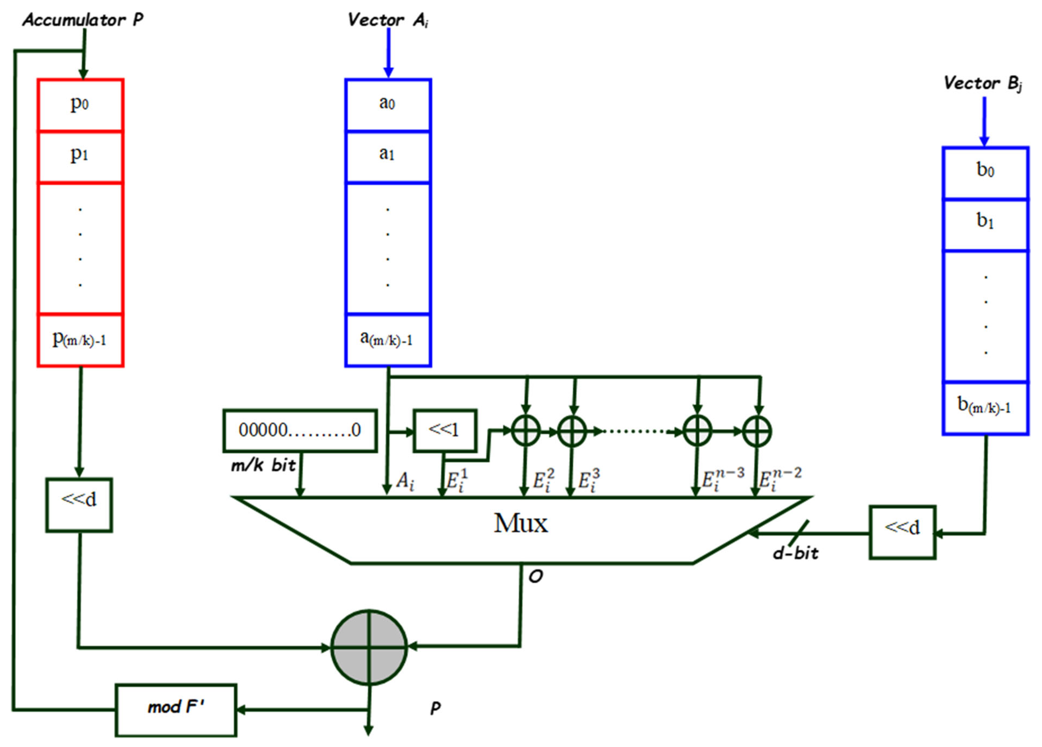
3.2. Digit-Serial Multiplier Algorithm and Design

Based on BPB representation approach, the multiplication of A(x) and B(x) can be expressed as:
C = A ( x ) B ( x ) m o d   F x = A ( x ) B 0 + B 1 x + + B k 1 x k 1 m o d   f ( x ) = A B 0 + A B 1 x + + A B k 1 x k 1   m o d   f ( x )
Since y = x k , we can obtain:
A ( 1 ) = A x = A 0 + A 1 x + + A k 1 x k 1 x   m o d ( y + x k ) = A k 1 x k + A 0 x + A 1 x 2 + + A k 2 x k 1 = A k 1 y + A 0 x + A 1 x 2 + + A k 2 x k 1
Hence for i   [ 1 , k 1 ] , A ( i ) can be expressed as:
A ( i ) = A x i m o d y + x k = A k 1 y + j = 0 k 2 A j x i + j
where y + x k is based on the definition of y = x k .
The following multiplication structure has been derived from the aforementioned formulas:
C 0 C 1 C k 1 = A 0 A 1 A k 1       A k 1 y A 0 A k 2       A k 2 y A k 1 y A k 3                     A 1 y A 2 y A 0 B 0 B 1 B k 1
For:
C 0 = A 0 B 0 = j = 0 m k 1 a k j y j j = 0 m k 1 b k j y j = a 0 + a k y + a 2 k y 2 + + a m k y m k 1 b 0 + b k y + b 2 k y 2 + + b m k y m k 1 = c 00 + c 01 y + c 02 y 2 + + c m k 1 y m k 1 ,
where we can define F x = x m 1 + x a + 1 = y m / k + x a + 1 + x to reduce the coefficient C 0 = A 0 B 0 .
Figure 2 depicts the suggested multiplier structure. It can be observed that A(x) and B(x) in GF(2m), by using BPB representation, are split into k sub-vectors (Ai, Bi) of (m/k) bits where ( i [ 0 ,   k 1 ] ). Then, using an mRnIM approach, the multiplication over polynomial lengths of ((m/k) − 1) bits is obtained. mRnIM is used to reduce the multiplier complexity.
We derive mRnIM from R2IM (Radix-2 Interleaved Modular Multiplication). It works on groups of d = log 2 n bits of B j , where each group represents one of n-possible values, as presented in Table 1 for n = 8.
mRnIM is defined as an iterative XOR of an accumulator P and the partial products   A i B j d , where B j d are d-bit of a multiplier B j . P is d-bit left-shifted, in every step, and then is reduced modulo F’. Depending on the d-bit of a multiplier B j , the accumulator P is conditionally XORED to the product ( A i B j d ). As shown in Table 1, the mRnIM technique decreases the overall iteration number from m/k to m/dk. As a consequence, multiplication time and required clock cycles are significantly reduced.
Algorithm 1 describes the mRnIM technique. The mRnIM method processes d-bits of a multiplier at a time, either shifting from MSB to LSB or vice versa. The potential partial products can be identified using d-bit regroupment: 0, 1, x, (x + 1),…, j = 0 d 1 x j . Algorithm 1 involves three major operations given as follows:
(d-bit left shift mod F′) operation, as specified in step 5.2.
Selecting the input to be XORED to the accumulator P based on the B i d B i d 1 bits of a multiplier B i (step 5.3).
XOR operation is specified in step 5.4.
Algorithm 1. Modifed Radix-n  G F ( 2 m / k ) Interleaved Multiplication algorithm.
  • Input: A i = a m k 1 ; a m k 2 ; ; a 0 ,   B i = b m k 1 ; b m k 2 ; ; b 0 ; d
  • Output: P = A i B i   m o d   F ( x )
  • Define; P = i = 0 2 m k 2 p i x i ; // p i = 0
  • Define;   E i 1 = S H L A i , 1 , E i 2 = E i 1 A i ,……,   E i n 1 = E i n 2 E i n 3 ; j = m k 1 ;
  • Multiplication step
    5.1.
    For i = m k d − 1 to 0 loop
    5.2.
    P = S H L P , d   m o d   F   ; // m o d u l a r   d o u b l i n g
    5.3.
    Switch ( B i j . . B i j d ) {
    • Case (0): O = ( o t h e r s = > 0 ) ;
    • Case (1): O = A i ;
    • Case (2): O = E i 1 ;
    • ….
    • Case (n): O = E i n 1 ; };
    5.4.
    P = P O   m o d   F ;  
    5.5.
    j = j n ;
    5.6.
    E n d   f o r
  • Return P
Figure 3 shows the mRnIM multiplication architecture. The shift-left operations are represented by <<n in the design.

3.3. Design Space Complexity

To compute the partial products, the suggested multiplier employs k mRnIM. Hence, the computation of the partial products involves ( n d 1 ) ( m k 1 ) XOR gates to calculate the precomputed values and one n:1 MUX ( S n × 1 m u x ) to select one of them. Moreover, (n − 1) number of S 2 × 1 m u x are used to construct the n:1 MUX. One S 2 × 1 m u x consists of two AND gates, one inverter gate, and one OR gate. Therefore, the space multiplier complexity ( S m M u l ) can be calculated as follows:
S m M u l = k n d 1 m k 1 X O R + S n × 1 m u x = k n d 1 m k 1 X O R + n 1 S 2 × 1 m u x = k n d 1 m k 1 X O R + n 1 ( 2 A N D + O R + I N V )
Due to processing d multiplier bits, (n − 2) values noted E i w where i   0 ,   k 1 and w [ 1 ,   n 2 ] are precomputed (step 5). Furthermore, in each iteration of step 5.2, one substep in 5.3 is performed. As a result, steps 5.2, 5.3, and 5.4 define the total data path. Therefore, 2 T + 1 T m u x m k d is the time necessary to complete the computation of partial products, where m k d represents the latency of the multiplier ( T indicates the delay time of an XOR gate). Consequently, the time complexity ( D m M u l ) of the multiplier is defined below:
D m M u l = ( 2 T + 1 T m u x ) m k d
To further validate the efficacy of the proposed design strategy, we have also synthesized the proposed digit-serial structure. Based on trinomial f’(x), we have coded the proposed design by Xilinx ISE 14.7 (Virtex 7-FPGA device). Table 2 summarizes the implementation results (area, time, area-delay product (ADP), and power) of BPB-mRnIM over GF(2m) (m = 163, 233, 283, 409, and 571).
As demonstrated in Table 2, the suggested multiplier (BPB-mRnIM) has a low power consumption, which is advantageous to resource-constrained devices. During the self-test at 50 MHz, BPB-mRnIM over GF(2571) consumes only 16.40 mW, 18.18 mW, and 20.45 mW when d = 4, 6, and 8 for k = 6, respectively. Furthermore as shown in Table 2, the lower ADP for m 283 is attained when (k,d) = (6.8).

4. Low-Cost ECC Processor Design and Implementation

The low-cost ECC processor computation operations were carried out over GF(2m) with m = 163, 233, 283, 409, 571. The architectural design characteristics of our proposed design are discussed in the subsections that follow.

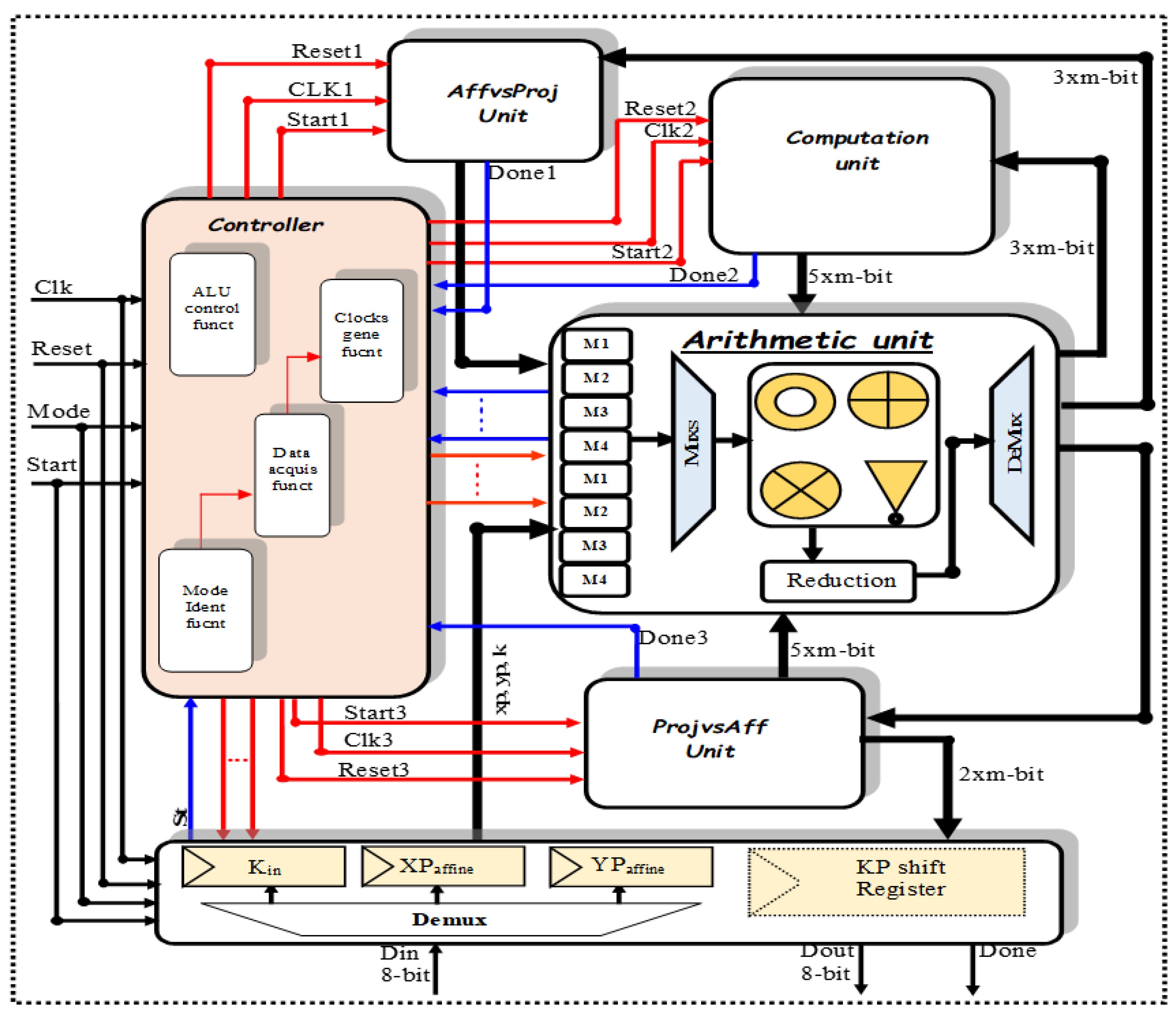
4.1. Low-Cost ECC Processor Design

The ECC design provided here is based on the use of projective coordinates, as seen in Figure 4. The fundamental goal of the design is to make use of the known concurrency in the point multiplication process in order to improve the efficiency of ECC while minimizing resource consumption. An input/output unit, an affine to projective unit, a projective to affine unit, a computation unit, an efficient arithmetic unit, and a specialized control unit comprise the design. The National Institute of Standards and Technology (NIST) was used to establish the initial curve parameters for the suggested design.

4.2. Processor Implementation

The suggested hardware architecture comprises of components that operate continuously. Scalar point multiplication operations are performed with the help of reliant on and no reliant operations. They can run concurrently or sequentially. This strategy will be used for all units. As shown in Figure 4, our suggested ECC processor for MPM employs one BPB-mRnIM multiplier to achieve the smallest area. The essential components of the ECC architecture will be discussed in detail in this section.

4.2.1. Bus Interface Unit

The input operands and final results are split into smaller bit length words of 8 bits in order to reduce input and output lengths and enable a word-by-word operation. The bus interface unit is controlled by four signals in the proposed design: start, reset, mode, and clock. The “mode” signal is used to configure the ECC processor and define the security requirements. As a consequence, the number of computing cycles required is proportional to the security level. For example, mode = “00” informs the computing unit that ECC-163 must be executed. Similarly, m = 233, 283, 409, and 571. When “start” is set and “mode” is fixed, 8 bits by 8 bits, XPaffine, YPaffine, and the key K (input data) are received and saved in the 3xm register file. To read and update the register file, a Mux and Demux are utilized. Finally, when the data conversion from projective to affine is completed, the results are sent out 8 bits by 8 bits. As a result, reading or writing m-bit block data takes (m/8) cycles on the bus interface unit.

4.2.2. Conversion Unit: Affine to Projective

The affine coordinates of a point P(XPaffin, YPaffine) will be converted by this unit to projective coordinates (X,Y,Z). It performed the entire conversion using one multiplier, one Galois field squarer, and XORs; it is based on the reuse of multiplier blocks and the storing of results in each step. When the input signals are received and “start1” is set, the AffvsProj begins the conversion process and provides the signal “done1” to the controller.

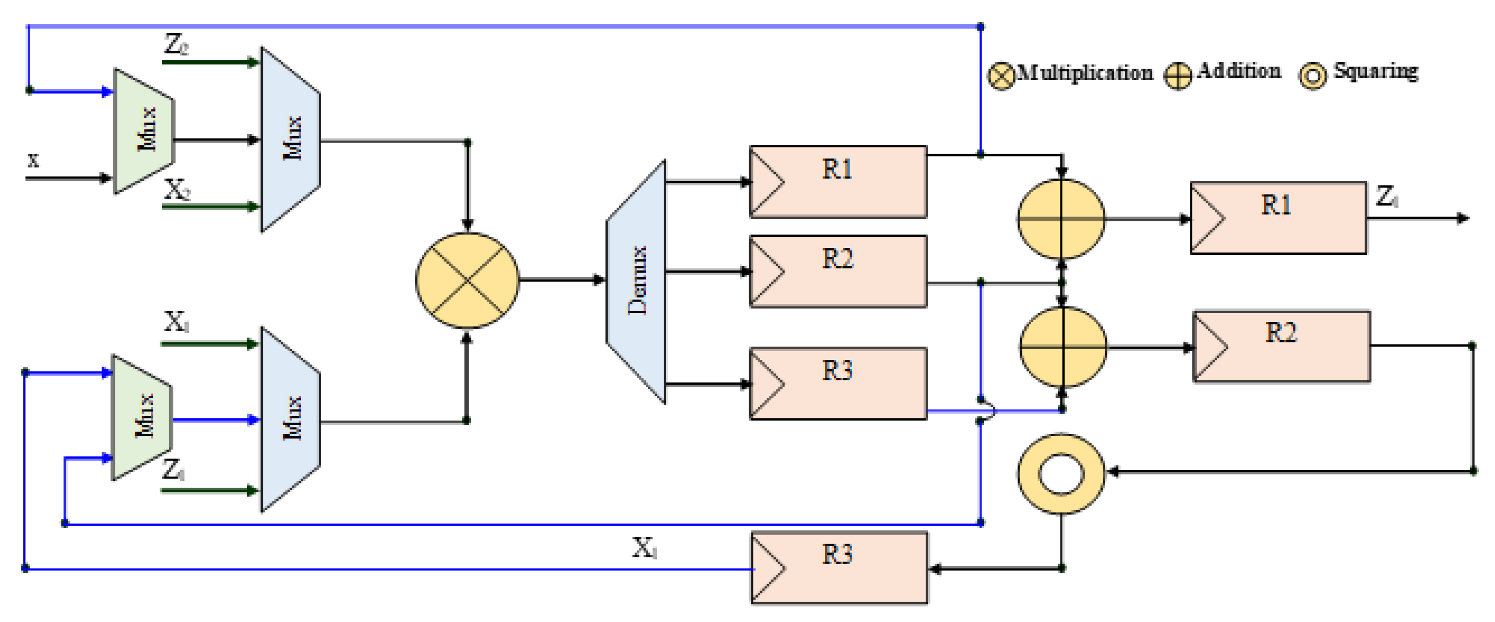
4.2.3. Arithmetic Unit

The arithmetic unit is the system’s lowest operation module. As illustrated in Figure 4, it is made up of a new digit-serial multiplier, two square blocks, one adder circuit, multiplexers, demultiplexer, and a register file. Mux has a length of 2 × 1, whereas Demux has a length of 1 × 2. As a memory block, the suggested dedicated 2-stage pipelined design employs an 8m register file. The registers are used for preserving the intermediate and final results of Algorithm 2 throughout and after execution. Using the relevant control signals, the various multiplexers read operands from the register file, while (Demux) is used to modify the contents of the register file with a particular register address.

4.2.4. Computation Unit

Two ways exist for performing the operation of adding points. The first one implies that Z1 is not equal to 1, which necessitates many square and field multiplication operations. Since Z1 is equal to 1, the second method is more effective and requires fewer steps. The second method is utilized for the point addition operation in this article, as we are developing an efficient ECC core for resource-constrained devices. Four square operations and nine field multiplications are necessary to add two points; while to perform a single ECC point doubling operation, four field multiplications and five square operations are required.
In this work, we propose a Modified LD-MPM over GF(2m), as seen in Algorithm 2. It consists of four phases: Firstly, initialization of inputs and output, secondly, conversing from affine to LD projective coordinate, thirdly, PA and PD computation in an LD projective coordinate which is the main loop, and finally, conversing from LD projective to affine coordinate. It computes both point doubling and point addition for every ki bit using only one multiplication performed on each step. Hence, the use of one multiplier reduced the area occupancy. To improve the clock frequency, we increase the number of pipeline stages. In our ECC design, PA and PD are combined. The advantage of PA–PD combination is to avoid data dependency. Based on the proposed modified algorithm, PD and PD computation depend on the next key bit ki+1. Such that when ki+1 = ‘1’, the step-output will be (X1, Z1), otherwise (X2, Z2) after step 2. When ki+1 = ‘0’, we start with the multiplication X1Z2 in step 1 and X2Z1 in step 2. In step S2, regardless of ki+1, the quad square output (Z2) is saved in the local register R1, while the square output (X2) is saved in the local register R2. From step 3, PA and PD follow the same instructions. Four multiplications are performed in step 3, 4, 5, and 6 respectively. The last multiplication is followed by an addition operation in step 6 to get the new X1. The dataflow of the PA and PD are shown in Figure 5 and Figure 6, respectively.
Algorithm 2. LD-Montgomery point multiplication modified algorithm (Mul, Sqr, ADD denote the multiplication, squaring, and addition, respectively).
Input:  k = ( k m 1 , . , k 1 , k 0 )   w i t h   k m 1 = 1 ; P = x , y E ( F 2 m )  
Output:  k p = ( x 3 , y 3 )
Initial Step:
P X 1 , Z 1 ( x , 1 ) ; 2 P = Q X 2 , Z 2 ( x 4 + b , x 2 )
For i from (m-2) to 0 do
If ki = ‘1’ then
If ki+1 = ‘1’ thenIf ki+1 = ‘0’ then
S-1: Z1 = Mul(X2,Z1);S-1: Z2 = Mul(X1,Z2);
S-2: X1 = Mul(X1,Z2)S-2: X2 = Mul(X2,Z1)
S-2: R1 = Sqr2(Z2); R2 = Sqr(X2);
S-3: X2 = Mul(b,R1); Z2 = Sqr(Z2); R4 = Sqr(R2); R3 = Add(X1,Z1);
S-4: Z2 = Mul(R2,Z2); Z1 = Sqr(R3); X2 = ADD(X2, R4);
S-5: R2 = Mul(x, Z1); R1 = X1; R3 = Z1
S-6: X1 = ADD(Mul(R1,R3), R2)
Conversion Step:
   x 3 ,   y 3 = ( X 1 Z 1 , x + X 1 Z 1 X 1 + x Z 1 X 2 + x Z 2 + x 2 + y Z 1 Z 2 x Z 1 Z 2 1 + y )
Furthermore, to reduce the power consumption in our compact ECC design, two techniques are adopted:
  • Clock gating: it minimizes power by introducing extra logic to a circuit in order to prune the clock tree [30].
  • Asynchronous counter: Many counters are used in our design. Since every register bit is activated on each clock edge, synchronous counters may consume a lot of power. Asynchronous counters only trigger the initial flip-flop using clk. Then the former flip-flops trigger later ones. Therefore, needless register changes may be eliminated and dynamic power may be reduced [31].
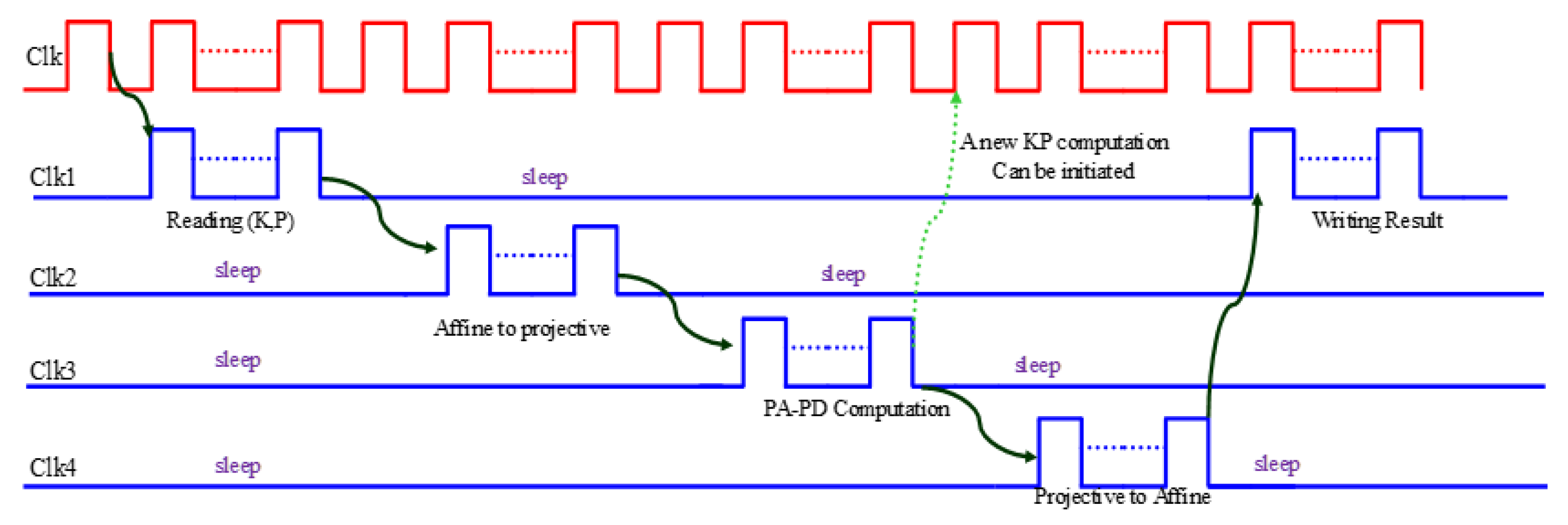
4.2.5. Control Unit

The control unit is designed to control the flow of data in the design, as well as the movement of data between the arithmetic unit and the others units. For PM computation, Algorithm 2 is implemented using an FSM-based dedicated controller. It provides the necessary control signals to all components. The data computation in Algorithm 2 requires 16 instructions distributed among multiplication (Mul: 8 instructions), addition (ADD: 3 instructions), and squaring (Sqr: 5 instructions). Out of these 16 instructions, 12 are executed regardless of the value of ki+1. During the initialization phase, the controller provides the control signals required by the bus interface unit for reading the input data (k, and P(x,y)). Once the data read operation is complete (“st” = ‘1’), the controller activates the “AffvsProj” unit via three signals (reset1, clk1, and start1). Once projective coordinates are calculated, the controller generates the computing unit control signals to begin the calculations. After a specific number of cycles, a generated point (X1, X2, Z1, Z2) is forwarded the ProjvsAff unit to be mapped into the affine coordination (x, y). Therefore, the control unit triggers the “ProjvsAff” unit to start the conversion step. Operands are saved in the register file during scalar multiplication calculation. Thus, the controller unit loads operands in each step, then saves the results to be utilized in the following operations till the scalar multiplication process is completed.
To ensure synchronization, we divided the control process into four functions: mode identification (specifying the Galois field size: m = 163, 233, 283, 409, or 571 and initialization parameters), data acquisition (to control the bus interface unit), clock generation, and ALU control. Figure 7 shows how the clock generating function generates CLKi and RESETi signals for ECC core units. The primary design clock generates four sub-clocks: clock1, clock2, clock3, and clock4 for the bus interface unit, AffvsProj unit, calculation unit, and ProjvsAff unit. This allows units to go into sleep mode when idle for reduced energy consumption.

4.2.6. Conversion Unit: Projective to Affine

When the “done2” signal is set by the computation unit, the controller activates the “ProjvsAff“ unit to convert the computation results. Only one multiplier, one square, and one inversion component are used in this unit. The controller then verifies “done3”, once true, the ProjvsAff- output is forwarded to the bus interface unit for additional processing.

4.2.7. Critical Path Delay and Clock Cycles

The data path is divided into three parts: affine to projective, point computation (doubling, adding), and projective to affine. The point computation contains eight registers for storing intermediate results. Each register has its own multiplexer for writing the value generated by the arithmetic unit. It should be noted that all registers, multipliers, squarer’s, multipliers, and inverters may be reconfigured based on the chosen finite field m. The suggested multiplier has a delay of v cycles where v = m / k d (one addition or squaring is executed in one clock cycle). Algorithm 2 illustrates that the point addition/doubling process requires six steps. The multiplication instruction requires v clock cycles in step 1. Step 2 involves doing one multiplication and two squaring operations in v clock cycles and one clock cycle, respectively. Similarly, a multiplication operation is continuously present in the subsequent phases. As a result, each step is carried out within v cycles. As a result, the overall latency of the point calculation module in projective coordinates is ≈6(m − 1) v . Hence, the total clock cycles for the proposed ECC processor are 2 v + 6 m 1 v + 2 m , where 2 v is for the initialization phase and 2m is for inversion. The simplified bit-level version of the EEA method is employed to accomplish the inversion operation in the proposed ECC processor architecture [19].

5. Results and Comparisons

An analysis is performed by the implementation of an FPGA design that efficiently performs ECC over GF(2m). We used the VHDL hardware description language to create our ECC processor. The design was synthesized, placed, and routed using target devices of Xilinx Virtex 5, Virtex 6, and Virtex 7. The Xilinx ISE timing closure techniques are used to achieve the best possible high-performance results. The starting parameter values utilized in our compact ECC core implementation are NIST elliptic curve recommendations. Table 3 shows the computed results, which include maximum frequency (Fmax, MHz), area utilization (Slices, LUTs), KP time (µs), and efficiency. The efficiency is calculated as follows:
E f f i c i e n c y = m ( b i t s ) A r e a ( S l i c e s ) × T i m e ( µ s )
The proposed ECC design on Virtex 5, Virtex 6, and Virtex 7 can compute KP over GF(2163) in 9.28 (µs), 8.8 (µs), and 8.39 (µs) and consumes 4368 LUTs, 3681 LUTs, and 3872 LUTs, respectively. Compared to Virtex 5 and Virtex 6, one also can see that the efficiency of the proposed design implemented on Virtex 7 is the highest. In addition, during a self-test at 50 MHz, the proposed ECC processor on Virtex 7 consumed only 39.5 mW, 56.6 mW, 80.83 mW over GF(2163), GF(2233), and GF(2283) respectively. The achievement of reduced area and high frequency is due to the efficiency of the proposed field multiplier.

5.1. Implementation Results over Small Field Sizes

The experimental results for small field sizes (m = 163, 233, and 283) have been presented in Table 3.

5.1.1. Implementation Results for GF(2163)

The architectures proposed by [11,15,32] are most like our design, based on one multiplier (1 × 163-bit). The efficiency of our architecture implemented on Virtex 7 is, respectively, 43%, 63%, and 35% higher than the best previous work [11,15,32]; while its KP time is, respectively, 6.77%, 21.8%, and 20.17% lower. As far as only the area is concerned, the proposed design shows the lowest area implementation. Our design respectively consumes 80.7%, 74.19%, and 75.85% less FPGA LUTS on Virtex 7 compared to [13,14,21]. Furthermore, the efficiency of our architecture is, respectively, 60%, 32%, and 32% higher than [13,14,21]. Likewise, the efficiency of our architecture, whether implemented on Virtex 5 or Virtex 6, is greater than [10,16].

5.1.2. Implementation Results over GF(2233)

In comparison to [19], which offers the smallest area implementation, our design consumes 74.39% more FPGA slices on Virtex 7. However, our design is 99.61% faster and the efficiency is 98% higher than [19]. Compared to [15,32] and based on the proposed digit-serial multiplier, our ECC design consumes less area. It saves 3593 slices and 521 slices, respectively. Moreover, our design achieves the highest efficiency when compared with all reported works and it is 10% higher than the highest efficiency in a previous work [32].

5.1.3. Implementation Results over GF(2283)

In comparison to [21], which has the lowest KP time, our design uses 2.69 time speed on the Virtex 7. However, the efficiency of our implemented design on Virtex 7 is 18% higher than [21]. As far as only the area is concerned, the proposed design shows the lowest area implementation. Compared to [15,21], it saves 3045 slices and 4934 slices, respectively. Compared to [10,12,33], our design implemented on Virtex 5 shows the higher efficiency.

5.2. Implementation Results over Large Field Sizes

The experimental results for the large field sizes (m = 409 and 571) have been presented in Table 3. Table 3 clearly shows that the suggested architecture outperforms the existing large field-size ECC solutions.

5.2.1. Implementation Results over GF(2409)

The efficiency of the proposed design is 3% higher than the highest efficiency in a previous work [21]; while, the required resources for our design is 60.49% lower than [21]. In comparison to [20], which has the lowest area implementation over GF(2409), our design saves 9.52% of FPGA slices and shows 8% efficiency improvement. As compared to [11,17] our design saves 41.69% and 63.9% of FPGA slices and shows 30% and 35% efficiency improvement, respectively. Moreover, our design implemented on Virtex 5 and Virtex 6 outperforms [10,12,33] in terms of efficiency.

5.2.2. Implementation Results over GF(2571)

Considering the maximum field size recommended by NIST, that is, GF(2571), the efficiency of the proposed design, whether on Virtex 7, Virtex 6 or Virtex 5 is higher than all the reported designs. In comparison to [20], which has the lowest area implementation over GF(2571), our design consumes 1.26% more FPGA Slices on Virtex 7. However, our design is 3.54% faster than [20] and shows 3% efficiency improvement. As compared to [11,14,17,21], our design saves 55.6%, 88.5%, 66.77%, and 58.25% of FPGA slices and shows 52%, 79%, 47%, and 10% efficiency improvement respectively.

6. Conclusions

In this paper, a digit-serial multiplier based on Bivariate Polynomial Basis representation and mRnIM technique has been used to perform a low-cost low-power point multiplication. The developed architecture has been implemented on the Xilinx Virtex 5, Virtex 6 and Virtex 7 FPGA devices resulting in the highest efficiency reported implementations over the small and large field sizes. The efficiency of the implemented architecture is 31%, 10%, 18%, 3%, and 3% higher than the highest efficiency in a previous work [21] (m = 163; m = 283; m = 409), [32] (m = 233), and [20] (m = 571), respectively. The proposed ECC design on Virtex 7 computes KP over GF(2163) in 8.39 (µs) and consumes 1071 slices; GF(2283) in 22.18 (µs) and consumes 2162 slices; GF(2409) (µs) in 39.77 and consumes 4016 slices; GF(2571) in 62.6 (µs) and consumes 5756 slices. Moreover, a comparison with the existing designs in the literature reveals that the suggested architectural design requires less area and consumes low power. This feature opens the door to the potential of employing our proposed design with resource-constrained devices.

Author Contributions

Conceptualization, M.Z.; methodology, M.Z. and A.S.; software, M.Z.; validation, A.S. and H.Y.A.; Simulation analysis, H.Y.A. and O.A.A.; writing—original draft preparation, M.Z. and A.S.; writing—review and editing, H.Y.A. and O.A.A.; supervision, M.Z. All authors have read and agreed to the published version of the manuscript.

Funding

This work was supported by the Deputyship for Research & Innovation, Ministry of Education in Saudi Arabia under research project (IF2/PSAU/2022/01/22010).

Data Availability Statement

Not applicable.

Acknowledgments

The authors extend their appreciation to the Deputyship for Research & Innovation, Ministry of Education in Saudi Arabia for funding this research work through project number IF2/PSAU/2022/01/22010.

Conflicts of Interest

The authors declare no conflict of interest.

References

  1. Astorga, J.; Barcelo, M.; Urbieta, A.; Jacob, E. Revisiting the Feasibility of Public Key Cryptography in Light of IIoT Communications. Sensors 2022, 22, 2561. [Google Scholar] [CrossRef]
  2. Miller, V.S. Use of elliptic curves in cryptography. In Proceedings of the Advances in Cryptology—CRYPTO’85, Santa Barbara, CA, USA, 18–22 August 1986; pp. 417–426. [Google Scholar]
  3. IEEE 1363-2000; Standard Specifications for Public Key Cryptography. IEEE Standards: Piscataway, NJ, USA, 2004.
  4. SEC2; Recommended Elliptic Curve Domain Parameters, Standards for Efficient Cryptography 2. Certicom Research: Mississauga, ON, Canada, 2010.
  5. Liu, Z.; Liu, D.; Zou, X.; Lin, H.; Cheng, J. Design of an Elliptic Curve Cryptography Processor for RFID Tag Chips. Sensors 2014, 14, 17883–17904. [Google Scholar] [CrossRef]
  6. Lee, D.-H.; Lee, I.-Y. A Lightweight Authentication and Key Agreement Schemes for IoT Environments. Sensors 2020, 20, 5350. [Google Scholar] [CrossRef] [PubMed]
  7. Awaludin, A.M.; Larasati, H.T.; Kim, H. High-Speed and Unified ECC Processor for Generic Weierstrass Curves over GF(p) on FPGA. Sensors 2021, 21, 1451. [Google Scholar] [CrossRef]
  8. Islam, M.M.; Hossain, M.S.; Hasan, M.K.; Shahjalal, M.; Jang, Y.M. Design and Implementation of High-Performance ECC Processor with Unified Point Addition on Twisted Edwards Curve. Sensors 2020, 20, 5148. [Google Scholar] [CrossRef]
  9. Sajid, A.; Sonbul, O.S.; Rashid, M.; Jafri, A.R.; Arif, M.; Zia, M.Y.I. A Crypto Accelerator of Binary Edward Curves for Securing Low-Resource Embedded Devices. Appl. Sci. 2023, 13, 8633. [Google Scholar] [CrossRef]
  10. Sutter, G.D.; Deschamps, J.P.; Imana, J.L. Efficient elliptic curve point multiplication using digit-serial binary field operations. IEEE Trans. Ind. Electron. 2013, 60, 217–225. [Google Scholar] [CrossRef]
  11. Khan, Z.U.A.; Benaissa, M. Throughput/area-efficient ecc processor using Montgomery point multiplication on FPGA. IEEE Trans. Circuits Syst. II Express Briefs 2015, 62, 1078–1082. [Google Scholar] [CrossRef]
  12. Li, L.; Li, S. High-performance pipelined architecture of elliptic curve scalar multiplication over GF(2m). IEEE Trans. Very Large Scale Integr. Syst. 2016, 24, 1223–1232. [Google Scholar] [CrossRef]
  13. Rashidi, B.; Sayedi, S.M.; Rezaeian Farashahi, R. High-speed Hardware Architecture of Scalar Multiplication for Binary Elliptic Curve Cryptosystems. Microelectron. J. 2016, 52, 49–65. [Google Scholar] [CrossRef]
  14. Khan, Z.U.A.; Benaissa, M. High-speed and low-latency ECC processor implementation over GF(2m) on FPGA. IEEE Trans. Very Large Scale Integr. Syst. 2017, 25, 165–176. [Google Scholar] [CrossRef]
  15. Imran, M.; Rashid, M.; Jafri, A.R.; Kashif, M. Throughput/area optimized pipelined architecture for elliptic curve crypto processor. IET Comput. Digit. Tech. 2019, 13, 361–368. [Google Scholar] [CrossRef]
  16. Harb, S.; Jarrah, M. FPGA implementation of the ECC over GF(2m) for small embedded applications. ACM Trans. Embed. Comput. Syst. 2019, 18, 1–19. [Google Scholar] [CrossRef]
  17. Lee, C.Y.; Zeghid, M.; Sghaier, A.; Ahmed, H.Y.; Xie, J. Efficient Hardware Implementation of Large Field-Size Elliptic Curve Cryptographic Processor. IEEE Access 2022, 10, 7926–7936. [Google Scholar] [CrossRef]
  18. Nadikuda, P.K.G.; Boppana, L. Low area-time complexity point multiplication architecture for ECC over GF(2m) using polynomial basis. J. Cryptogr. Eng. 2023, 13, 107–123. [Google Scholar] [CrossRef]
  19. Aljaedi, A.; Jamal, S.S.; Rashid, M.; Alharbi, A.R.; Alotaibi, M.; Alanazi, D.J. Area-Efficient Realization of Binary Elliptic Curve Point Multiplication Processor for Cryptographic Applications. Appl. Sci. 2023, 13, 7018. [Google Scholar] [CrossRef]
  20. Rashid, M.; Sonbul, O.S.; Zia, M.Y.I.; Kafi, N.; Sinky, M.H.; Arif, M. Large Field-Size Elliptic Curve Processor for Area-Constrained Applications. Appl. Sci. 2023, 13, 1240. [Google Scholar] [CrossRef]
  21. Zeghid, M.; Ahmed, H.Y.; Chehri, A.; Sghaier, A. Speed/Area-Efficient ECC Processor Implementation Over GF(2m) on FPGA via Novel Algorithm-Architecture Co-Design. IEEE Trans. Very Large Scale Integr. Syst. 2023, 31, 1192–1203. [Google Scholar] [CrossRef]
  22. Xie, J.; Kumar Meher, P.; Sun, M.; Li, Y.; Zeng, B.; Mao, Z.H. Efficient FPGA Implementation of Low-Complexity Systolic Karatsuba Multiplier over GF(2m) Based on NIST Polynomials. IEEE Trans. Circuits Syst. I 2017, 64, 1815–1825. [Google Scholar] [CrossRef]
  23. Pan, J.; Song, P.; Yang, C. Efficient digit-serial modular multiplication algorithm on FPGA. IET Circuits Devices Syst. 2018, 12, 662–668. [Google Scholar] [CrossRef]
  24. Lee, C.; Xie, J. Digit-Serial Versatile Multiplier Based on a Novel Block Recombination of the Modified Overlap-Free Karatsuba Algorithm. IEEE Trans. Circuits Syst. I 2019, 66, 203–214. [Google Scholar] [CrossRef]
  25. Heidarpur, M.; Mirhassani, M. An Efficient and High-Speed Overlap-Free Karatsuba-Based Finite-Field Multiplier for FGPA Implementation. IEEE Trans. Very Large Scale Integr. Syst. 2021, 29, 667–676. [Google Scholar] [CrossRef]
  26. Li, H.; Ren, S.; Wang, W.; Zhang, J.; Wang, X. A Low-Cost High-Performance Montgomery Modular Multiplier Based on Pipeline Interleaving for IoT Devices. Electronics 2023, 12, 3241. [Google Scholar] [CrossRef]
  27. Menezes, A.J.; van Oorschot, P.C.; Vanstone, S.A. Handbook of Applied Cryptography; CRC Press: Boca Raton, FL, USA, 2018. [Google Scholar]
  28. Hankerson, D.; Menezes, A. Elliptic curve cryptography. In Encyclopedia of Cryptography, Security and Privacy; Springer: Berlin/Heidelberg, Germany, 2021; pp. 1–2. [Google Scholar]
  29. Harkelson, D.; Menezes, A.; Vanstone, S. Guide to Elliptic Curve Cryptography; Springer: New York, NY, USA, 2004; pp. 75–152. [Google Scholar]
  30. Wu, Q.; Pedram, M.; Wu, X. Clock-Gating and its application to low power design of sequential circuits. IEEE Trans. Circuits Syst. I Fundam. Theory Appl. 2000, 47, 415–420. [Google Scholar] [CrossRef]
  31. Wei, D.; Zhang, C.; Cui, Y.; Chen, H.; Wang, Z. Design of a low-cost low-power baseband-processor for UHF RFID tag with asynchronous design technique. In Proceedings of the 2012 IEEE International Symposium on Circuits and Systems (ISCAS), Seoul, Republic of Korea, 20–23 May 2012. [Google Scholar]
  32. Imran, M.; Pagliarini, S.; Rashid, M. An Area Aware Accelerator for Elliptic Curve Point Multiplication. In Proceedings of the 2020 27th IEEE International Conference on Electronics, Circuits and Systems (ICECS), Glasgow, UK, 23–25 November 2020. [Google Scholar]
  33. Zhao, X.; Li, B.; Zhang, L.; Wang, Y.; Zhang, Y.; Chen, R. FPGA Implementation of High-Efficiency ECC Point Multiplication Circuit. Electronics 2021, 10, 1252. [Google Scholar] [CrossRef]
Figure 1. Arithmetic operations in ECC hierarchy.
Electronics 12 04110 g001
Figure 2. Digit-serial multiplier (BPB-mRnIM) structure.
Electronics 12 04110 g002
Figure 3. mRnIM GF(2m/k) proposed partial multiplier.
Electronics 12 04110 g003
Figure 4. Low-cost ECC processor design.
Electronics 12 04110 g004
Figure 5. Point doubling data flow.
Electronics 12 04110 g005
Figure 6. Point addition data flow.
Electronics 12 04110 g006
Figure 7. Clock generating process.
Electronics 12 04110 g007
Table 1. mR8IM encoded steps and instructions.
B j d B j d 1 B j d 2 Partial ProductsPrecomputed ValuesEncoded StepsEncoded Instructions
0000-3-bit left shiftP=SHL(P,3)
0011-3-bit left shift, ⨁ A i P=SHL(P,3)⨁ A i
010x E i 1 = 1-bit A i left shift3-bit left shift, ⨁ E i 1 P=SHL(P,3)⨁ E i 1
011x+1 E i 2 = E i 1   A i 3-bit left shift, ⨁ E i 2 P=SHL(P,3)⨁ E i 2
100x2 E i 3 = 2-bit A i left shift3-bit left shift, ⨁ E i 3 P=SHL(P,3)⨁ E i 3
101x2+1 E i 4 = E i 3   A i 3-bit left shift, ⨁ E i 4 P=SHL(P,3)⨁ E i 4
110x2+x E i 5 = E i 3   E i 1 3-bit left shift, ⨁ E i 5 P=SHL(P,3)⨁ E i 5
111x2+x+1 E i 6 = E i 5   A i 3-bit left shift, ⨁ E i 6 P=SHL(P,3)⨁ E i 6
Table 2. Proposed multiplier complexities on FPGA platform (Virtex 7).
GF(2m)LUTsFrequency
(MHz)
Computation
Time (ns)
Power
mW
ADP(10−6)
(k,d) = (6,4)
m = 163570499.52327.194.17513
m = 233820484.24340.16.6629
m = 2831006425.41250.679.8546
m = 4091465415.36978.2912.14100
m = 5711774413.317112.4116.40166
(k,d) = (6,6)
m = 163804445.31620.345.4513
m = 2331145434.73929.788.17529
m = 2831391429.82736.5811.9544
m = 4091998405.79555.9914.2784
m = 5712353395.84780.1418.18140
(k,d) = (6,8)
m = 163968414.27516.398.58515
m = 2331387395.824.5312.6930
m = 2831906391.3330.1314.95540
m = 4092440357.74447.6416.4583
m = 5712909351.44267.720.45137
Table 3. Comparison to related ECC architectures (T.W denotes this work).
Ref.GF(2m)FPGA
Virtex
Area
(Slices)
LUTsFFsFreq
(MHz)
KP Time (µs)Efficiency
(×103)
Efficiency (%)
[10]1635615022,936-2505.54.8274
[18]1635-12,566-2613.9--
[16]163622055864717630642.461.7591
[11]163714764721188639710.5110.5143
[13]16375575--4373.977.3760
[14]1637415014,20237473523.1812.3632
[21]1637443516,34545902792.9312.5531
[15]163722079965198136910.736.8963
[32]163715294162-383911.8535
T.W16351205436811523509.2814.5719
T.W16361073368111413698.817.264.8
T.W16371071387211413878.3918.14
[19]23373912346-16144500.13498
[15]2337512018,953276435715.782.8968
[32]233720486407-379148.1310
T.W2337152755481626356178.98
[10]2835709625,030-18833.61.1980
[12]2835628620,256-21319.92.2762
[33]2835-116,241-13522.36--
[15]2837520720,202321033720.322.6855
[21]2837709628,03378722418.244.8518
T.W283524139277231628925.404.6121
T.W283721627924230033122.185.91
[10]409510,23628,503-164102.60.3985
[12]409511,51335,31313,84317219.41.8429
[33]4096-116,241-13541.36--
[11]4097688820,881603831632.721.8230
[17]409711,12937,69717,70116821.951.6835
[20]4097443912,568412935738.942.378
[21]409710,16640,15311,27422416.42.463
T.W4095448113,733430523345.572.00322
T.W4096370911,701427424443.512.542
T.W4097401611,730427526739.772.57
[12]571518,82858,66519,38012736.50.8448
[10]5715870730,718-128352.50.1989
[33]5716-11,624-13556.5--
[16]5716673819,15824,730261189.10.4572
[14]571750,336141,07829,21711134.050.3479
[11]571712,96538,54710,06625057.610.7752
[20]5717568314,356596131764.821.563
[17]571717,32457,27823,35114738.890.8547
[19]571713,78954,47013,27521828.81.4410
T.W5715642219,263531219874.881.1825
T.W5716525616,413527420771.631.515
T.W5717575616,454527522762.61.59
Disclaimer/Publisher’s Note: The statements, opinions and data contained in all publications are solely those of the individual author(s) and contributor(s) and not of MDPI and/or the editor(s). MDPI and/or the editor(s) disclaim responsibility for any injury to people or property resulting from any ideas, methods, instructions or products referred to in the content.

