Article

Low-Power Single Bitline Load Sense Amplifier for DRAM

1
School of Integrated Circuits, Anhui University, Hefei 230601, China
2
Anhui Provincial High-Performance Integrated Circuit Engineering Research Center, Hefei 230601, China
3
Key Laboratory of Intelligent Computing and Signal Processing of Ministry of Education, Anhui University, Hefei 230601, China
*
Author to whom correspondence should be addressed.
Electronics 2023, 12(19), 4024; https://doi.org/10.3390/electronics12194024
Submission received: 18 August 2023 / Revised: 15 September 2023 / Accepted: 20 September 2023 / Published: 25 September 2023
(This article belongs to the Special Issue CMOS Integrated Circuits Design)

Abstract

:
With the significant growth in modern computing systems, dynamic random access memory (DRAM) has become a power/performance/energy bottleneck in data-intensive applications. Both the power management mechanism and downscaling method face decreasing performance or difficulties in the smaller footprint of the DRAM capacitor. Since optimizing the circuit of sense amplifier (SA) is an efficient method to reduce energy consumption, we propose two single bitline load sense amplifier (SBLSA) circuits, i.e., a redundant voltage discharged SBLSA (RVD-SBLSA) circuit and a bit aware SBLSA (BA-SBLSA) circuit, to improve conventional and single bitline write (SBW) circuits. The RVD-SBLSA circuit utilizes a clamp diode to discharge redundant voltage over VDD/2 with an additional working stage. The BA-SBLSA circuit abandons the single bitline load (SBL) circuit during read and write ‘1’ operations. The RVD-SBLSA circuit can offer the lowest total energy consumption, and the BA-SBLSA circuit can make a better balance between energy consumption and latency. Through the simulation results, the proposed circuits can efficiently reduce energy consumption or balance energy consumption and latency and show huge potentials in very large-scale integrated circuits.

1. Introduction

The volatile memory of static random access memory (SRAM) and dynamic random access memory (DRAM) are widely used in computing systems [1,2,3,4]. Scaling bulk CMOS SRAM technology for on-chip caches beyond the 22 nm node results in high leakage power consumption, performance degradation, and instability due to process variations [5,6]. Benefiting from vertical multi-gate devices (FinFETs) and 2T/3T1D types of DRAM, embedded DRAMs are candidates to substitute SRAM in very large-scale integrated (VLSI) circuits [7], due to the DRAM having higher densities and lower cell leakage current in sleep mode. There are different kinds of cell types of DRAM, like 1T1C, 2T, 3T1C, 3T1D, etc. Though other types of DRAM show advantages over 1T1C cell in read and write operations, the mostly used 1T1C cell has the smallest cell area, showing the best memory density compared to other DRAM cells [8]. With the significant growth in modern computing systems, DRAM has become a power/performance/energy bottleneck in data-intensive applications [9,10,11]. Power consumption is a major issue in low-power and portable devices. New types of DRAM, like 2T and 3T1D, have been analyzed and compared, the results show that the minimum-energy point can be reduced by increasing the length of write transistor/boosting write word-line/using high-threshold voltage write transistor methods [12]. Furthermore, the power management mechanism and downscaling method are useful to reduce the energy consumption of DRAM. A new refresh scheme of DRAM, which can refresh with its own refresh period without requiring the external support, shows efficacy in enhancing energy efficiency [13]. In particular, downscaling DRAM shows better performance, less power dissipation and less read/write delays [14]. However, this comes at the cost of decreasing performance or facing difficulties in the smaller footprint of the DRAM capacitor. The performance of a 1T1C DRAM cell is affected due to various leakage sources in the MOS transistor [7]. Leakage is a crucial issue in DRAM, which will bring about the probability of data loss from storage capacitor increase and deteriorate the retention time [15]. Furthermore, optimizing the circuit of the sense amplifier (SA) is an efficient and convenient method to reduce the overall energy consumption of DRAM during some particular operations [16,17].
As shown in Figure 1, a conventional sensing circuit of 1T1C DRAM is composed of an SA circuit, a precharge circuit, a write circuit, an isolation circuit and DRAM arrays [11,18]. In a typical SA circuit, the orange color part comprises two cross-coupled inverters, a PMOS and a NMOS transistor. The input and output nodes of the SA are attached to the BL and BLB bitlines, respectively. When either one is selected as a target bitline, the other one is accordingly selected as the reference bitline. The precharge circuit is comprised of three NMOS transistors controlled by the PRE signal. At each operation cycle, the bitlines are charged to VDD/2 before accessing the DRAM cells [19]. The bitline nodes at the IO interface can transfer the amplified voltage to the IO bus or be driven by the write drivers with the help of IO transistors. Isolation transistors are only placed in a folded array structure to isolate SAs from different arrays for reuse [20,21].
Based on the conventional sensing circuit, a low power single bitline write (SBW) sensing circuit with reconfigurable I/O interface was also proposed [22,23]. The block turns off one of the isolation transistors to form single bitline load (SBL) circuit when the SA or write driver tries to drive a reference bitline from VDD/2 to VDD [24]. The SBW circuit turns off the isolation transistors connected to the reference bitlines during whole read and write operation, with the limited applications in the open bitline array, which lacks isolation transistors [25]. Furthermore, the SBW circuit generates greater energy consumption and time delay than a conventional circuit in a consecutive precharge stage.
In this study, we analyzed the different SA working stages and the energy consumption of DRAM arrays during different read and write operations. Then, we built a single bitline load sense amplifier and simulated its performance. Furthermore, we propose two improved SBLSA circuits to overcome some drawbacks existent in SBL circuits. Simulations indicate that both circuits consume less energy than conventional circuits no matter whatever data they read or write.

2. Methods

2.1. The Energy Consumption at Different Working Stages

Using the Formula (1) to qualitatively describe power consumption at different working stages, the actual power consumption was carried out by the product of voltage and the time integral of the current from the circuit simulations.
W = U × Δ Q = U × T 1 T 2 I d t

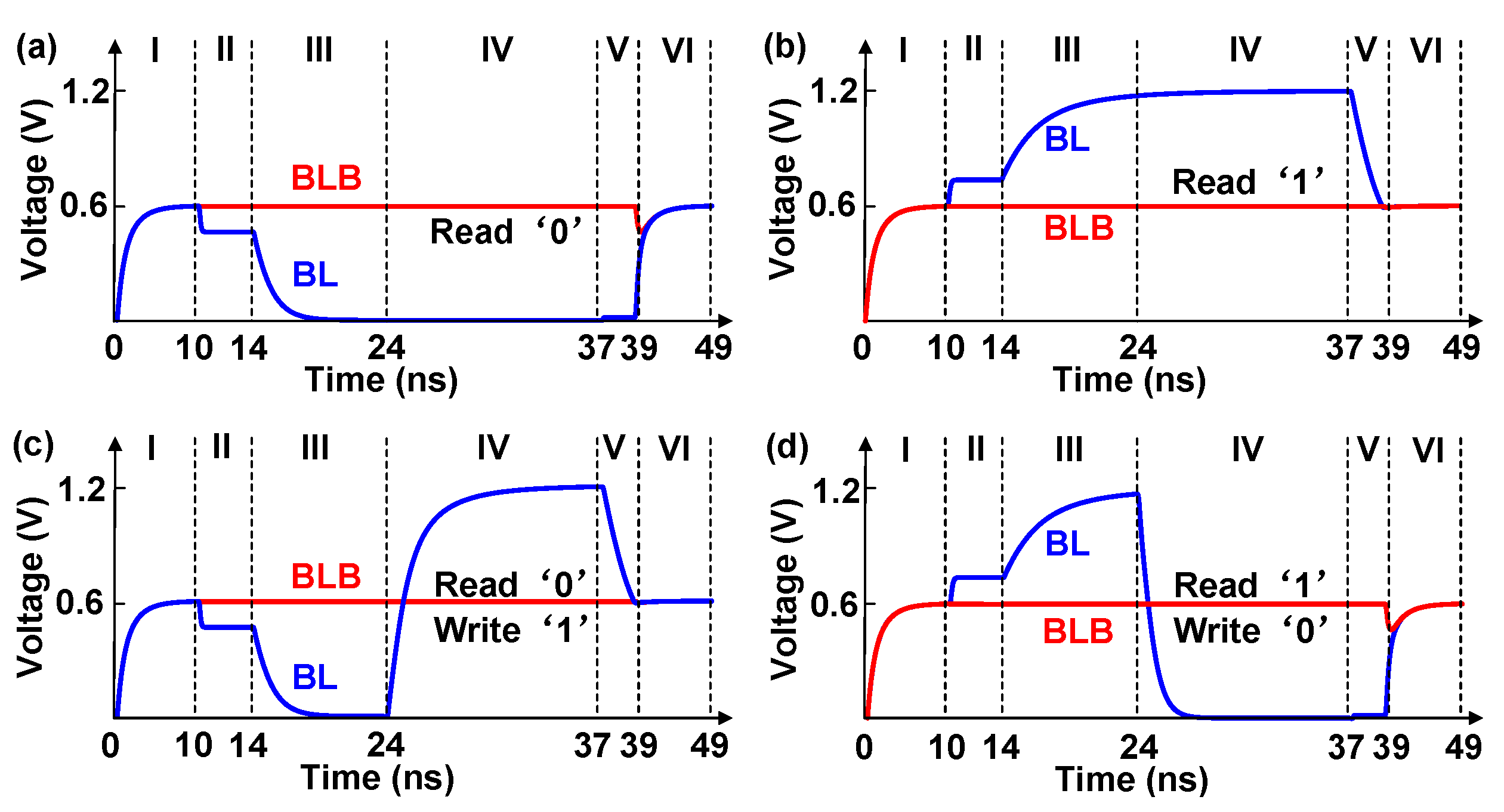
2.1.1. Precharge Stage

Each reading and writing cycle begins with a precharge stage, where both the BL and BLB with load capacitance Cb are biased at VDD/2 by the precharge circuit, assuming the initial voltage of the bitlines is zero. Energy consumption in the precharge stage can be defined as (VDD2Cb)/2 [26]. As shown in Figure 2, the bitline voltage is recovered to VDD/2 over the whole cycle. As a result, when an array is consecutively accessed, the bitlines are precharged and equilibrated to VDD/2 to form a full swing voltage, and this process is defined as a consecutive precharge stage. Owing to the dynamic charge transfer between BL and BLB, the energy consumption in the consecutive precharge stage is measured by the time integral of the current.

2.1.2. Pre-Sense and Post-Sense Stage

When the word line (WL) signal is turned on, the charge sharing between storage capacitors and the BL leads to a voltage variation (ΔV). There is no energy consumption in the pre-sense stage. While in the post-sense stage, the sense amplifier senses and amplifies ΔV to VDD, i.e., charging the BL to VDD and discharging the BLB to ground [27]. Theoretically, the energy consumption is (VDD2Cb)/2 for both the logic 0 and 1 states.

2.1.3. IO Transition Stage

In the IO transition stage, the data stored in the DRAM cells are identified based on the voltage on the bitlines. When the IO transistors are turned on, the data stored in the cells can be read out or modified through read/write operations [28,29]. The situation that the write data are matched with the stored data (read ‘0’-write ‘0’ and read ‘1’-write ‘1’) is not considered in the read–modify–write operation, since the energy consumption is supplied by an external circuit. During the write operation (read ‘0’-write ‘1’), where the write driver charges the BL and the storage capacitor (Cs) to VDD, the energy consumption is calculated as VDD2(Cb+Cs). Similarly, for read ‘1’-write ‘0’, where the write driver charges the BLB to VDD, the energy consumption is VDD2Cb.

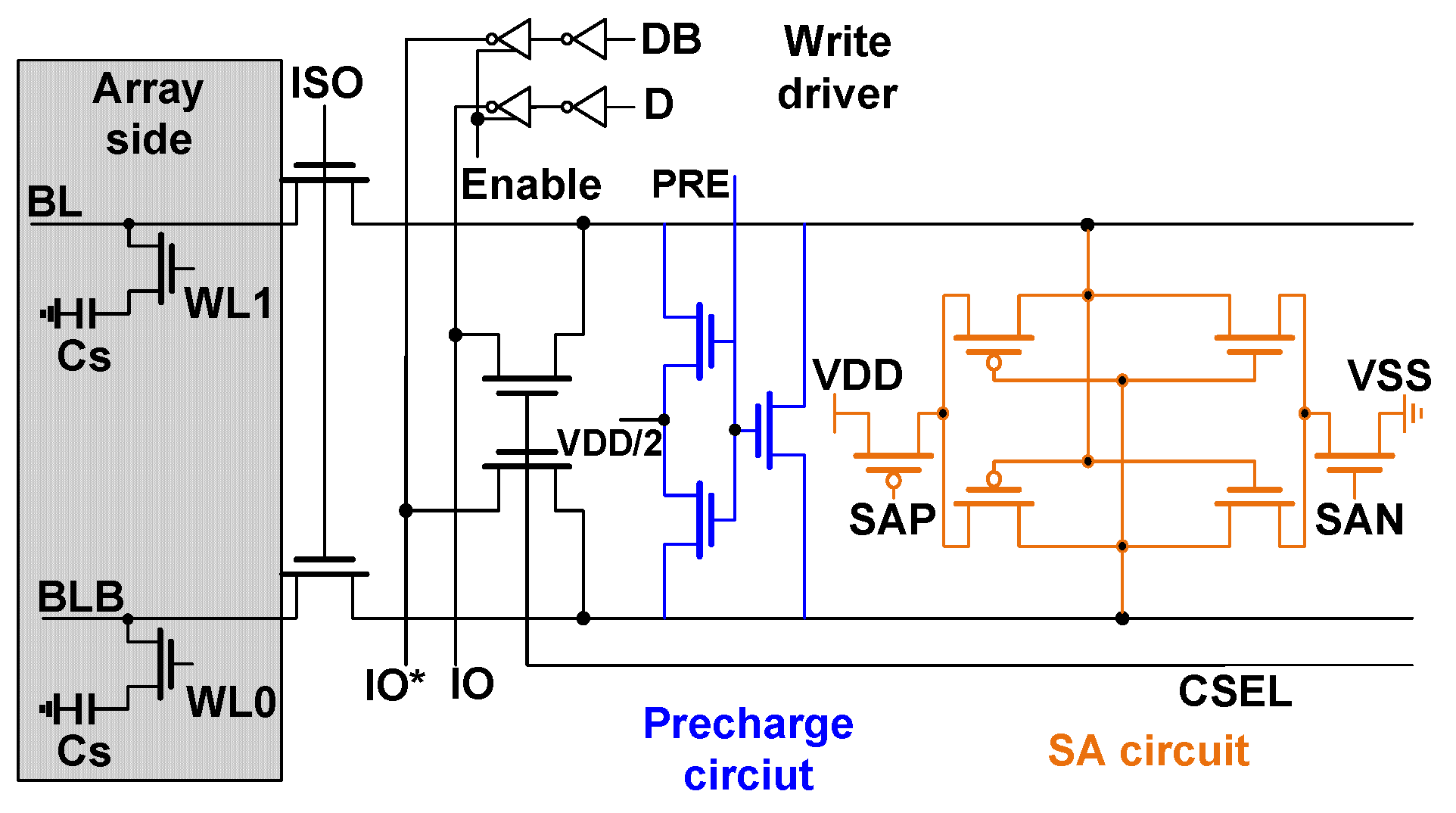
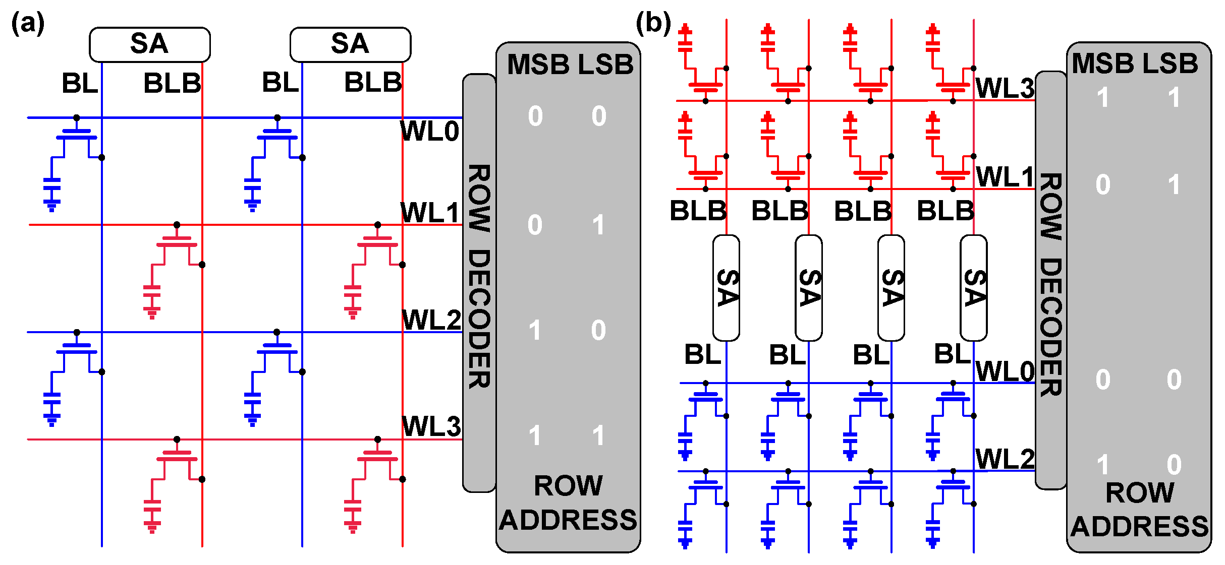
2.2. Analysis of the Single Bitline Load Sense Amplifier

In an SBW circuit, the reference bitline is isolated from the SA and the precharge circuit by reusing the existing isolation transistors to reduce energy consumption in Macro (Figure 3a) [22]. During the read process, the precharge stage charges the BL and BLB to VDD/2, forming ∆V in the pre-sense stage. But in the post-sense stage, the BL and BLB are isolated from the SA to save the energy of amplifying the BL/BLB from ∆V to VDD. And in rewriting stage, the data are written only through the BL. However, the isolated transistor needs an additional control signal. Considering the necessity of isolation transistors in bitline arrays, the SBW circuit is only applicable to folded bitline arrays. As shown in Figure 3b, we proposed a single bitline load sense amplifier (SBLSA) circuit with added isolated switches to analyze the energy consumption at different stages. The switches are used to isolate the SA from the reference bitline and the precharge circuit. Though energy consumption in the precharge stage is inevitable, the voltage supply from the SA is not required to charge the BLB to VDD, thereby (VDD2Cb)/2 can be reduced in the post-sense stage. Similarly, during a read ‘1’-write ‘0’ operation, there is no voltage supply requirement for charging the BLB capacitance Cb from the write driver, resulting in reduced VDD2Cb in the IO transition stage. The newly added switches can be controlled by the least significant bit (LSB) of the row address line. The LSB signal can be latched and the reference bitline can be disconnected from the SA by turning off switch1 or switch2. In this study, the BL and BLB are, respectively, considered as target bitlines when LRA (LSB of the row address) is logic 0 and 1.
As shown in Figure 4, whether the folded or open bitline array are selected, every row address can be decoded and mapped to certain wordlines (e.g., WL0, WL1, WL2 and WL3) and bitlines (BL, BLB). This method builds a mapping relationship between the wordlines and bitlines, that is, WL0 and WL2 are mapped to BL, and WL1 and WL3 are mapped to BLB.
In both read or write operations, different from the full swing voltage in a conventional circuit, the SBLSA circuit makes reference and target bitlines achieve half swing voltage, owing to this the BLB remains constant at VDD/2. Bitline voltage swings from 0 to VDD/2 are termed negative half swings, and bitline voltage swings from VDD/2 to VDD are termed positive half swings. Compared with the full swing voltage, the half swing voltage shows two disadvantages. On the one hand, the SBLSA circuit generates greater energy consumption than a conventional circuit in a consecutive precharge stage. As shown in Figure 5, the area (time integral of current), which represents the energy consumption, of A1 is less than that of A2 and A3. On the other hand, when the SBLSA circuit reads or writes ‘1’, it requires a longer time to precharge the target bitline from VDD to VDD/2, i.e., T3 is longer than T1 and T2. To solve these problems, we propose two SBLSA circuits, i.e., the redundant voltage discharged SBLSA (RVD-SBLSA) and the bit aware SBLSA (BA-SBLSA) circuits, which can balance the latency and energy consumption well.

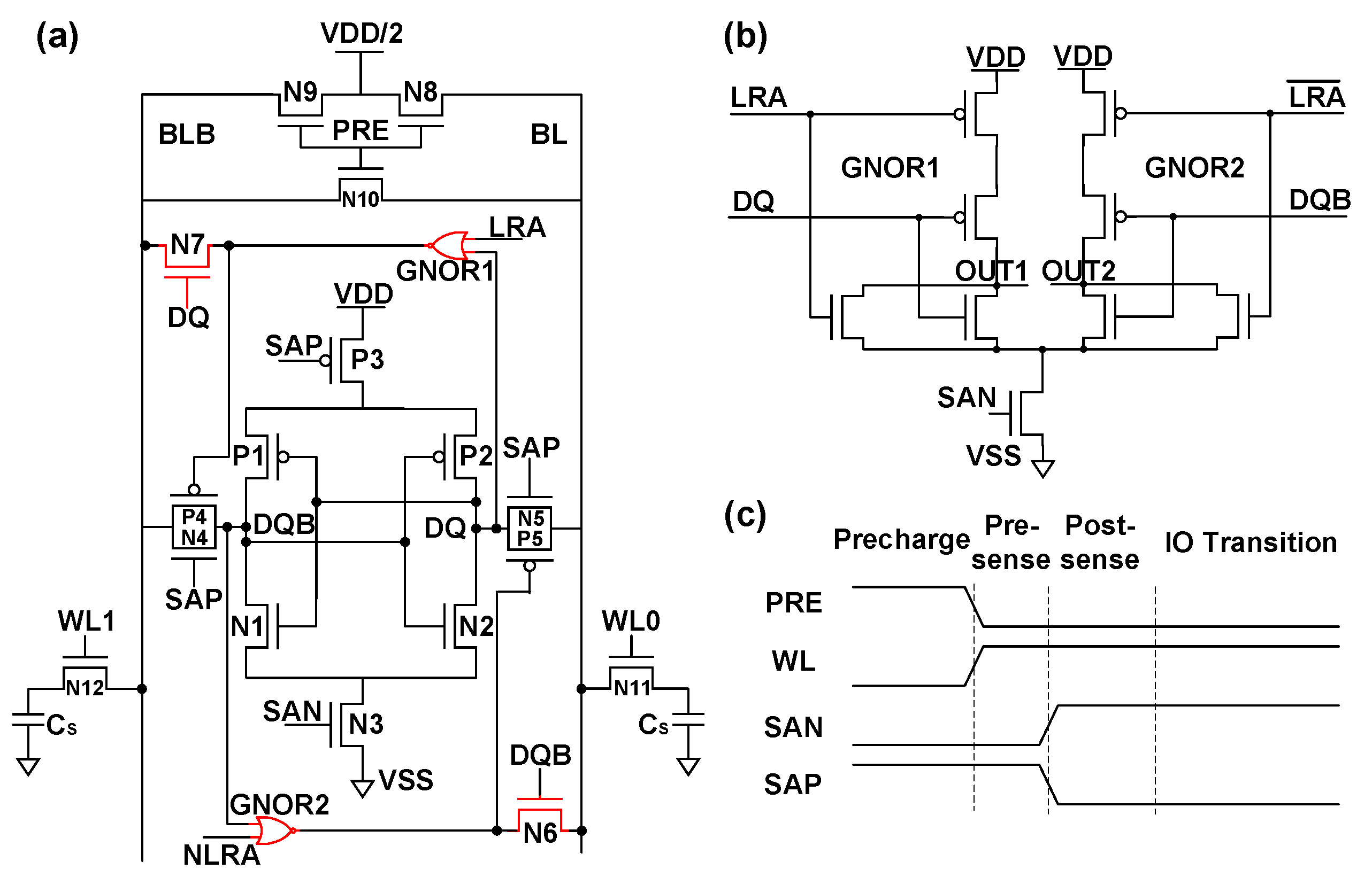
2.3. Redundant Voltage Discharge Sense Amplifier

Figure 6a shows the RVD-SBLSA circuit, where switch1 is composed of transistors N4 and P4, and switch2 is composed of N5 and P5. Compared with a conventional circuit, the additional parts are displayed in blue. As shown in Figure 6b, the RVD-SBLSA circuit performs the same functions as the SBLSA circuit. At the beginning of the post-sense stage, the SAN signal is low and both bitlines are connected to nodes DQ and DQB. As the SAN signal turns high, the switches are controlled by the address line signals of LRA and NLRA.
After the IO transition stage, an additional stage is required for discharging the redundant bitline voltage greater than VDD/2 during the read ‘1’ operation. For this reason, two NMOS transistors (N6 and N7) are used to form two diodes in an RVD-SBLSA circuit, and the bitline voltage is clamped at VDD/2. Thus, VDD/2 can drive both bitlines in the consecutive precharge stage without energy consumption during read ‘1’ and read ‘0’-write ‘1’ operations. As seen from the waveforms of the bitline voltage during different stages (Figure 7), the latency of the discharge and consecutive precharge stages can still be shorter than that of the SBLSA at the consecutive precharge stage.

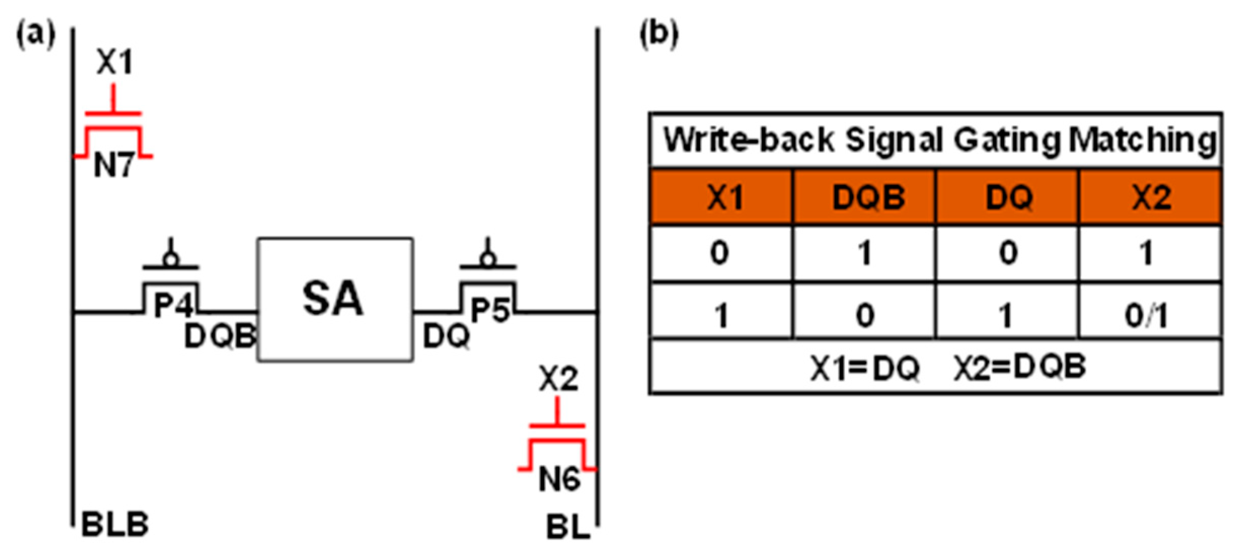
2.4. Bit Aware Sense Amplifier

To further solve the two disadvantages discussed in an SBLSA circuit during the read ‘1’ operation, a new solution was proposed, which uses a double-ended bitline load during read ‘1’, and using a single-ended bitline load in other cases. As shown in Figure 8a, the BA-SBLSA circuit comprises two switches, two logic control gates (GNOR1, GNOR2), and two auxiliary write-back transistors (N6, N7). Compared with a BA-SBLSA circuit, the additional parts of a BA-SBLSA circuit are shown in red. An LRA signal is capable of identifying the target and reference bitlines. In addition, DQ and DQB need to be identified in the SRAM cell. GNOR is a NOR gate (Figure 8b), where the two inputs are DQ/DQB and the LRA signal. GNOR is used to control the operation mode of the write-back operation. At the beginning of the post-sense stage, switch1 and switch2 are closed to amplify the DQ and DQB nodes to the corresponding voltage. Hence, the amplified DQ and DQB represent the data stored in the cell. When the LRA is low, the BL is the target bitline and BLB is the reference bitline, then P4 will be turned off when DQ is logic 0 and turned on when DQ is logic 1, respectively, while P5 keeps the target bitline connecting with the SA. It is vice versa when the LRA is high. And the signal waveforms are shown in Figure 8c.

Bit-Aware and Write-Back Logic

Considering switch1 (P4) and switch2 (P5) are not transmission gates, there is a threshold voltage loss during transmitting logic 1 and 0. The placement of the auxiliary write-back transistors, N6 and N7 coupled with P5 and P4, can form complementary transistors. In the post-sense stage, N5 and N4 are off, and the GNOR logic gate decides whether to turn P4 and P5 on or turn off. Cooperating with N6 and N7, the data can be written back to the bitline and the DRAM cell without voltage loss.
During the read or write ‘0’ operation, the write-back operation should ensure the reference bitline disconnects from the SA; while during the read or write ‘1’ operation, the reference bitline should connect with the SA, which is same as a conventional SA. The control logic design is as follows. As shown in Figure 9a, when ‘0’ is read, i.e., the DQ and DQB will be logic 0 and 1, the X1 transistor will be turned off to ensure the GNOR output does not affect the reference bitline. At the same time, the X2 transistor will be turned on to successfully transmit logic 0 using the NMOS. In another case of reading ‘1’, DQ and DQB are logic 1 and 0, respectively, and signal X1 is turned on to transmit logic 0. Considering that the complementary PMOS can transmit logic 1, it shows no effect whether the X1 is turned on or turned off. These results show that we can reuse the DQ and DQB value as the control signals for X1 and X2, respectively (Figure 9b).
Based on the logic and circuit design, the waveforms of bitline voltage at different stages are depicted in Figure 10. During the read ‘1’ and read ‘0’-write ‘1’ operations, the BL and BLB show full wing voltage, which resolves the problems of larger energy consumption and longer time in the consecutive precharge stage.

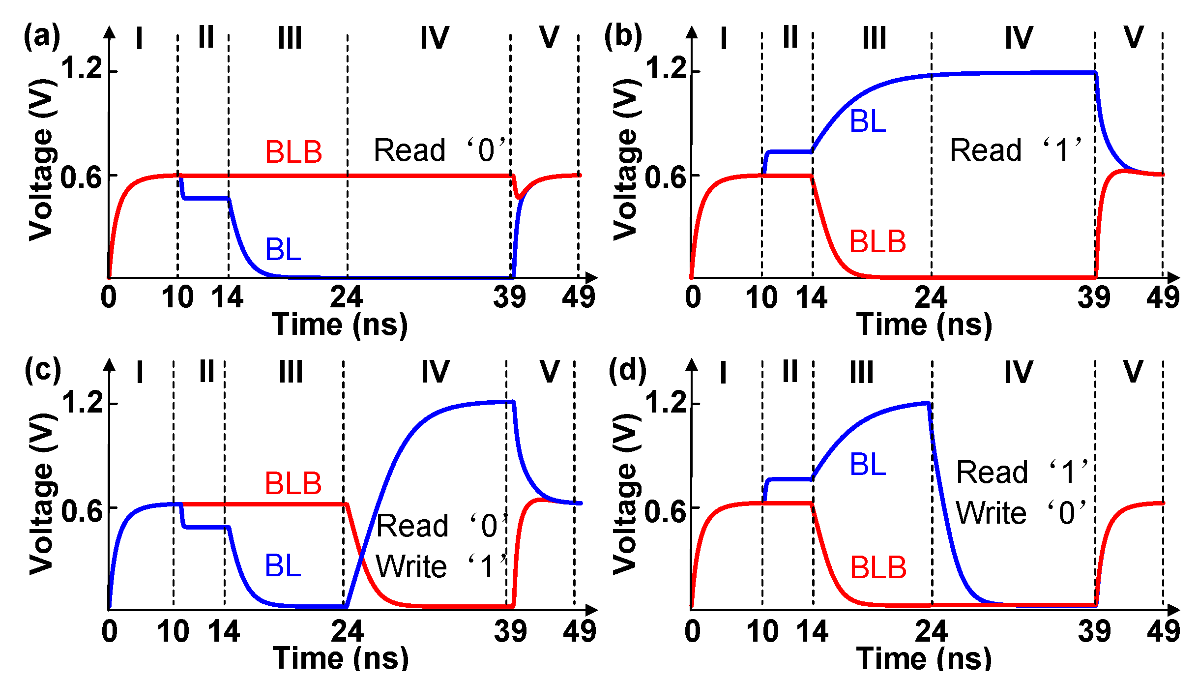
3. Results and Discussion

These circuits were simulated in a 65 nm CMOS process design kit at 1.2 V and 25 °C. The bitline capacitance is 100 fF, and the storage cell capacitance is 30 fF. As shown in Figure 11a, compared with that of a conventional SA circuit, all the SBW, RVD-SBLSA and BA-SBLSA circuits show much reduced energy consumption during read ‘0’ operations, where the consecutive precharge stage is predominant. During read ‘1’, read ‘0’-write ‘1’ and read ‘1’-write ‘0’ operations (Figure 11b–d), both the RVD-SBLSA and BA-SBLSA circuits still show reduced energy consumption, while the SBW circuit shows increased energy consumption in the read ‘1’ operation, which is one disadvantage of the positive half swing voltage. In the case of SBLSA circuits, in read ‘1’ and read ‘0’-write ‘1’ operations (Figure 11b,c), the RVD-SBLSA and BA-SBLSA circuits show reduced energy consumption mainly in the consecutive precharge stage, and the RVD-SBLSA exhibits the lowest energy consumption. This is because the two proposed structures, RVD-SBLSA, put the voltage of the target bitline to VDD/2 in the IO transmission stage, thus avoiding the huge energy consumption caused by the positive half swing voltage in the continuous pre-charging stage. The BA-SBLSA switches single/double bitline load mode using a logic judgment circuit, so as to balance low power consumption and low latency (Figure 12). Furthermore, the energy consumptions under different processes and temperatures show the same tendency (Table 1). To compare with the state-of-the-art results of SA in DRAM, the power consumption, which is in accordance with references, only contains read ‘0’ and ‘1’ operations. The proposed two circuits show better performance with less power consumption at different process technologies (Table 2).
As shown in Figure 12, the SBW circuit requires the longest time to drive the VDD to VDD/2 in the consecutive precharge stage. Compared to the conventional SA circuit, the latency of tRCD+tRP increased by 30.1% for the SBW circuit, 25.0% for the RVD-SBLSA circuit and 5.8% for the BA-SBLSA circuit. Considering the energy consumption and latency, the RVD-SBLSA circuit can give the best energy performance, and the BA-SBLSA circuit can give a better balance between them. Considering the area consumption, the layouts of conventional, RVD-SBLSA and BA-SBLSA circuits are shown in Figure 13. The areas of the RVD-SBLSA and BA-SBLSA circuits are 1.6 and 5.6 times larger, respectively, than a conventional circuit.

4. Conclusions

In conclusion, we have analyzed the working stages and energy consumption of DRAM arrays during different read and write operations through simulations. The SBW circuit consumes more energy than a conventional SA circuit during read ‘1’ operations and needs a longer precharge latency for the target bitline. The RVD-SBLSA circuit achieves significantly reduced energy consumption by adding two discharge transistors with a discharge stage. The BA-SBLSA circuit improves latency through a write-back structure without additional timing control. Both RVD-SBLSA and BA-SBLSA circuits realize reduced energy consumption in any read and write operations. The stimulations show that the RVD-SBLSA circuit generates the lowest energy consumption and the BA-SBLSA circuit provides a better balance between energy consumption and latency. The areas of the RVD-SBLSA and BA-SBLSA circuits are 1.6 and 5.6 times larger than conventional circuits, respectively. Due to the possibility that parasitic capacitance may affect the charge sharing, the performance of RVD-SBLSA and BA-SBLSA circuits may deteriorate. In future works, detailed post-simulation and the chip performance should be measured and compared to give a more in-depth study. These results provide a new method for reducing energy consumption in DRAM arrays and these circuits show huge potential in very large-scale integrated circuits.

Author Contributions

Conceptualization, X.W. and C.P.; validation, C.D. and Y.L.; data curation, Y.L. and W.L.; writing and editing, C.D. and Z.L.; funding acquisition, W.L., Z.L., X.W. and C.P. All authors have read and agreed to the published version of the manuscript.

Funding

This work was supported by Joint Funds of the National Natural Science Foundation of China under Grant U19A2074, Science Fund for Distinguished Young Scholars of Anhui Province under Grant 2108085J35, National Natural Science Foundation of China under Grant 62104001, Key Research and Development Program of Anhui Province under Grant 2022a05020044, and Open Project Fund of the Ministry of Education Key Laboratory of Intelligent Computing and Signal Processing under Grant 2020A004.

Data Availability Statement

The data that support the findings of this study are available from the corresponding author upon reasonable request.

Conflicts of Interest

The authors declare no conflict of interest.

References

  1. Kim, Y.; Yoo, C. Crosstalk Cancelling Voltage-Mode Driver for Multi-Gbps Parallel DRAM Interface. Int. J. Circuit Theory Appl. 2015, 43, 1175–1182. [Google Scholar] [CrossRef]
  2. Ravichandiran, P.P.; Franzon, P.D. A Review of 3D-Dynamic Random-Access Memory based Near-Memory Computation. In Proceedings of the IEEE International 3D Systems Integration Conference(3DIC), Raleigh, NC, USA, 26–29 October 2021; pp. 1–6. [Google Scholar]
  3. Hasan, S.S.; Imam, N.; Kannan, R.; Yoginath, S.; Kurte, K. Design Space Exploration of Emerging Memory Technologies for Machine Learning Applications. In Proceedings of the IEEE International Parallel and Distributed Processing Symposium Workshops (IPDPSW), Portland, OR, USA, 17–21 June 2021; pp. 439–448. [Google Scholar]
  4. Kim, Y.J.; Kwon, H.J.; Doo, S.Y.; Ahn, M.; Kim, Y.H.; Lee, Y.J.; Kang, D.S.; Do, S.G.; Lee, C.Y.; Cho, G.H.; et al. A 16-Gb, 18-Gb/s/pin GDDR6 DRAM with Per-Bit Trainable Single-Ended DFE and PLL-Less Clocking. IEEE J. Solid-State Circuits 2019, 54, 197–209. [Google Scholar] [CrossRef]
  5. Bhoj, A.N.; Jha, N.K. Gated-Diode FinFET DRAMs: Device and Circuit Design-Considerations. ACM J. Emerg. Technol. Comput. Syst. 2010, 6, 1–32. [Google Scholar] [CrossRef]
  6. Lin, C.H.; Greene, B.; Narasimha, S.; Cai, J.; Bryant, A.; Radens, C.; Narayanan, V.; Linder, B.; Ho, H.; Aiyar, A.; et al. High performance 14 nm SOI FinFET CMOS technology with 0.0174 µm2 Embedded DRAM and 15 levels of Cu metallization. In Proceedings of the IEEE International Electron Devices Meeting, San Francisco, CA, USA, 15–17 December 2014; pp. 3.8.1–3.8.3. [Google Scholar]
  7. Amat, E.; Calomarde, A.; Moll, F.; Canal, R.; Rubio, A. Feasibility of Embedded DRAM Cells on FinFET Technology. IEEE Trans. Comput. 2016, 65, 1068–1074. [Google Scholar] [CrossRef]
  8. Lim, D.Y.; Jung, I.J.; Kim, D.H.; Jung, S.O. Computing-in-Memory Using 1T1C Embedded DRAM Cell with Micro Sense Amplifier for Enhancing Throughput. In Proceedings of the IEEE International Conference on Consumer Electronics-Asia, Yeosu, Republic of Korea, 26–28 October 2022; pp. 1–4. [Google Scholar]
  9. Hamzaoglu, F.; Arslan, U.; Bisnik, N.; Ghosh, S.; Lal, M.B.; Lindert, N.; Meterelliyoz, M.; Osborne, R.B.; Park, J.; Tomishima, S.; et al. A 1 Gb 2 GHz Embedded DRAM in 22 nm Tri-gate CMOS Technology. In Proceedings of the IEEE International Solid-State Circuits Conference Digest of Technical Papers (ISSCC), San Francisco, CA, USA, 9–13 February 2014; pp. 230–231. [Google Scholar]
  10. Prasad, G.; Sahu, D.; Chandra Mandi, B.; Ali, M. Novel Low-Power and Stable Memory Cell Design using Hybrid CMOS and MTJ. Int. J. Circuit Theory Appl. 2022, 50, 465–477. [Google Scholar] [CrossRef]
  11. Kim, S.M.; Song, B.; Jung, S.O. Sensing Margin Enhancement Technique Utilizing Boosted Reference Voltage for Low-Voltage and High-Density DRAM. IEEE Trans. Very Large Scale Integr. (VLSI) Syst. 2019, 27, 2413–2422. [Google Scholar] [CrossRef]
  12. Rana, M.; Canal, R.; Amat, E.; Rubio, A. Statistical Analysis and Comparison of 2T and 3T1D e-DRAM Minimum Energy Operation. IEEE Trans. Device Mater. Reliab. 2017, 17, 42–51. [Google Scholar] [CrossRef]
  13. Choi, H.; Hong, D.; Lee, J.; Yoo, S. Reducing DRAM Refresh Power Consumption by Runtime Profiling of Retention Time and Dual-Row Activation. Microprocess. Microsyst. 2020, 72, 102942. [Google Scholar] [CrossRef]
  14. Raghavendra, M.; Jha, S.; Pavan, R.; Hemanth, S. Comparative Analysis of MOSFET and FinFET DRAM N*N Array. In Proceedings of the International Conference for Emerging Technology (INCET), Belgaum, India, 27–29 May 2022; pp. 1–7. [Google Scholar]
  15. Sankpal, A.S.; Pethe, D.J. Study and Analysis of Retention Time and Refresh Frequency in 1T1C DRAM at Nanometer Regime. In Micro and Nanoelectronics Devices, Circuits and Systems: Select Proceedings of MNDCS; Springer: Singapore, 2022; pp. 449–458. [Google Scholar]
  16. Kumar, A.; Pandey, A.; Sahu, P.K. Design of DRAM Sense Amplifier using 45 nm technology. In Proceedings of the International Symposium on Devices, Circuits and Systems (ISDCS), Howrah, India, 29–31 March 2018; pp. 1–5. [Google Scholar]
  17. Saini, A.; Gupta, P.K.; Gupta, R. Analysis of Low Power SRAM Sense Amplifier. In Proceedings of the International Conference on Electrical, Electronics and Computer Engineering (UPCON), Aligarh, India, 8–10 November 2019; pp. 1–6. [Google Scholar]
  18. Kim, D.H.; Song, B.; Ahn, H.A.; Ko, W.; Do, S.; Cho, S.; Kim, K.; Oh, S.H.; Joo, H.Y.; Park, G.; et al. A 16 Gb 9.5 Gb/S/pin LPDDR5X SDRAM with Low-Power Schemes Exploiting Dynamic Voltage-Frequency Scaling and Offset-Calibrated Readout Sense Amplifiers in a Fourth Generation 10 nm DRAM Process. IEEE Int. Solid-State Circuits Conf. (ISSCC) 2022, 26, 448–450. [Google Scholar]
  19. Huang, P.; Chang, K.C.; Ge, J.; Peng, C.; Wu, X.; Chen, J.; Lin, Z. Offset-Compensation High-Performance Sense Amplifier for Low-Voltage DRAM Based on Current Mirror and Switching Point. IEEE Trans. Circuits Syst. II Express Briefs 2022, 69, 2011–2015. [Google Scholar] [CrossRef]
  20. Kim, S.M.; Song, B.; Jung, S.O. Imbalance-Tolerant Bit-Line Sense Amplifier for Dummy-Less Open Bit-Line Scheme in DRAM. IEEE Trans. Circuits Syst. I Regul. Pap. 2021, 68, 2546–2554. [Google Scholar] [CrossRef]
  21. Rohbani, N.; Darabi, S.; Sarbazi-Azad, H. PF-DRAM: A Precharge-Free DRAM Structure. In Proceedings of the IEEE 48th Annual International Symposium on Computer Architecture (ISCA), Valencia, Spain, 14–18 June 2021; pp. 126–138. [Google Scholar]
  22. Kook, J.; Yoo, H.J. A Low Power Reconfigurable I/O DRAM Macro with Single Bit Line Writing Scheme. In Proceedings of the 26th European Solid-State Circuits Conference, Stockholm, Sweden, 19–21 September 2000; pp. 192–195. [Google Scholar]
  23. Na, T.; Song, B.; Choi, S.; Kim, J.P.; Kang, S.H.; Jung, S.O. Offset-Canceling Single-Ended Sensing Scheme with One-Bit-Line Precharge Architecture for Resistive Nonvolatile Memory in 65-nm CMOS. IEEE Trans. Very Large Scale Integr. (VLSI) Syst. 2019, 27, 2548–2555. [Google Scholar] [CrossRef]
  24. Subramanian, L.; Vaidyanathan, K.; Nori, A.; Subramoney, S.; Karnik, T.; Wang, H. Closed yet Open DRAM: Achieving Low Latency and High Performance in DRAM Memory Systems. In Proceedings of the ACM/ESDA/IEEE Design Automation Conference (DAC), San Francisco, CA, USA, 24–29 June 2018; pp. 1–6. [Google Scholar]
  25. Olgun, A.; Patel, M.; Yağlıkçı, A.G.; Luo, H.; Kim, J.S.; Bostancı, F.N.; Vijaykumar, N.; Ergin, O.; Mutlu, O. QUAC-TRNG: High-Throughput True Random Number Generation Using Quadruple Row Activation in Commodity DRAM Chips. In Proceedings of the IEEE 48th Annual International Symposium on Computer Architecture (ISCA), Valencia, Spain, 14–18 June 2021; pp. 944–957. [Google Scholar]
  26. Li, Y. Robust Design of DRAM Core Circuits: Yield Estimation and Analysis by a Statistical Design Approach, München. Ph.D. Thesis, Technische Universität, Munich, Germany, 2011. [Google Scholar]
  27. Hwang, C.L.; Kirihata, T.; Wordernan, M.; Fifield, J.; Storaska, D.; Pontius, D.; Fredernan, G.; Ji, B.; Tomashot, S.; Dhong, S. A 2.9 ns Random Access Cycle Embedded DRAM with a Destructive-Read. In Proceedings of the Symposium on VLSI Circuits, Honolulu, HI, USA, 13–15 June 2002; pp. 174–175. [Google Scholar]
  28. Jang, J.; Shin, W.; Choi, J.; Suh, J.; Kwon, Y.; Kim, Y.; Kim, L.S. Refresh-Aware Write Recovery Memory Controller. IEEE Trans. Comput. 2017, 66, 688–701. [Google Scholar] [CrossRef]
  29. Park, Y.H.; Choi, S.; Yoo, H.J. Bit-Wise Read-Compare-Write Scheme for Low Power Read-Modify-Write DRAM Operation. Electron. Lett. 2002, 38, 62–63. [Google Scholar] [CrossRef]
  30. Kim, T.B.; Kwon, K.W. Quick and Efficient Offset Compensation by Noise-Aware Operation of DRAM Bit Line Sense Amplifier, International Technical Conference on Circuits/Systems. In Proceedings of the Computers and Communications (ITC-CSCC), Phuket, Thailand, 5–8 July 2022; pp. 497–500. [Google Scholar]
Figure 1. Schematic diagram of a conventional sensing circuit and a 1T1C DRAM array. IO* means inverted signal of IO.
Electronics 12 04024 g001
Figure 2. Output waveforms of bitlines of a conventional sensing circuit in (a) read ‘0’, (b) read ‘1’, (c) read ‘0’-write ‘1’ and (d) read ‘1’-write ‘0’ operations. I: precharge stage; II: pre-sense stage; III: post-sense stage; IV: IO transition stage; V: consecutive precharge stage.
Electronics 12 04024 g002
Figure 3. (a) Read operation with an SBW circuit at charging sharing, differential and rewriting stages [22]; (b) The schematic diagram of an SBLSA circuit.
Electronics 12 04024 g003
Figure 4. Row address mapping relationship in (a) folded bitline and (b) open bitline array structures.
Electronics 12 04024 g004
Figure 5. Plot of current versus time for three swing voltages during the consecutive precharge stage.
Electronics 12 04024 g005
Figure 6. (a) Schematic diagram and (b) signal waveforms of an RVD-SBLSA circuit.
Electronics 12 04024 g006
Figure 7. Output waveforms of the bitlines of an RVD-SBLSA circuit in (a) read ‘0’, (b) read ‘1’, (c) read ‘0’-write ‘1’ and (d) read ‘1’-write ‘0’ operations. I: precharge stage; II: pre-sense stage; III: post-sense stage; IV: IO transition stage; V: discharge stage; VI: consecutive precharge stage.
Electronics 12 04024 g007
Figure 8. (a) Schematic diagram, (b) GNOR model and (c) signal waveforms of a BA-SBLSA circuit.
Electronics 12 04024 g008
Figure 9. (a) Write-back complementary transistors, and (b) the relationship between signal X and the data node.
Electronics 12 04024 g009
Figure 10. Output waveforms of bitlines of a BA-SBLSA circuit in (a) read ‘0’, (b) read ‘1’, (c) read ‘0’-write ‘1’ and (d) read ‘1’-write ‘0’ operations. I: precharge stage; II: pre-sense stage; III: post-sense stage; IV: IO transition stage; V: consecutive precharge stage.
Electronics 12 04024 g010
Figure 11. Energy consumption and different stage ratios of conventional, SBW, RVD-SBLSA and BA-SBLSA circuits in (a) read ‘0’, (b) read ‘1’, (c) read ‘0’-write ‘1’ and (d) read ‘1’-write ‘0’ operations.
Electronics 12 04024 g011
Figure 12. Latency of conventional, SBW, RVD-SBLSA and BA-SBLSA circuits.
Electronics 12 04024 g012
Figure 13. Layouts of (a) conventional, (b) RVD-SBLSA and (c) BA-SBLSA circuits. The areas of conventional, RVD-SBLSA and BA-SBLSA circuits are 3.0 μm2, 4.9 μm2 and 17.0 μm2, respectively.
Electronics 12 04024 g013
Table 1. Comparison of the energy consumptions of four structures under different processes and temperatures.
Energy Consumption (fJ)
OperationRead ‘0’Read ‘1’Read ‘0’-Write ‘1’Read ‘1’-Write ‘0’
Process corner/
Temperature (°C)
FF/
−40
TT/
25
SS/
125
FF/
−40
TT/
25
SS/
125
FF/
−40
TT/
25
SS/
125
FF/
−40
TT/
25
SS/
125
Conventional113.8116.4121.5113.8116.4121.2365.7366.4371.1333.0334.3339.1
SBW67.568.771.1146.5146.3146.9278.0276.0271.8160.4163.5161.6
RVD-SBLSA
(this work)
69.170.473.0109.299.691.7231.2215.3208.5159.0160.0155.8
BA-SBLSA
(this work)
70.170.873.1109.1113.8120.0242.2242.1245.7217.6219.4222.5
Table 2. Feature summary and comparison to other works.
BRV-SA [10] aCSC-SA [19] a*P1 [30]Conventional SA bSBW [14] bRVD-SBLSA
(This Work)
BA-SBLSA
(This Work)
Process (nm)652818065656565
VDD (V)1.00.90.81.21.21.21.2
Power consumption (μW)6.4410.73108.813.092.922.312.50
a: from references; b: evaluation under 65 nm process.
Disclaimer/Publisher’s Note: The statements, opinions and data contained in all publications are solely those of the individual author(s) and contributor(s) and not of MDPI and/or the editor(s). MDPI and/or the editor(s) disclaim responsibility for any injury to people or property resulting from any ideas, methods, instructions or products referred to in the content.

