Abstract
With the rapid development of information technology, the demand for high-speed and low-power technology for digital signal processing is increasing. Full adders and multipliers are the basic components of signal processing technology. Pass-transistor logic is a promising method for implementing full adder and multiplier circuits due to the low count of transistors and low-power characteristics. In this paper, we present a novel full adder based on pass transistors. The proposed full adder consists of 18 transistors. The post-layout simulation shows a 13.78% of power reduction compared to conventional CMOS full adders. Moreover, we propose an 8-bit signed multiplier based on the proposed full adder. The post-layout simulation shows an 8% power reduction compared to the multiplier produced by the Design Compiler synthesis tool. Compared to the existing work with a similar process, our work achieved only 19.02% of the power-delay product and 3.5% of the area-power product.
1. Introduction
With the rapid development and wide application of information technology, signal processing algorithms are widely being used in portable wireless devices, such as smartphones, PCs, and wearable devices. Full adders and multipliers are fundamental components in digital signal processing applications [1], such as convolution, fast Fourier transform (FFT) [2,3], finite impulse response (FIR) [4,5], discrete cosine transform (DCT) [6,7], infinite impulse response (IIR) filters [8], and audio/video codecs. Conventional multipliers are becoming the bottleneck of low-power digital signal processing applications [9,10].
Generally, multipliers could be classified into various types, such as array [11,12], Booth [13,14], carry-save, and Wallace tree [15,16], according to the methods used to produce, pass, and compress the partial products. In an array multiplier, the partial product is generated by the one-bit multiplication of the multiplicand and multiplier, mostly conducted by AND gates. The partial products are directly summed up by an array of adders. The array multiplier has an explicit structure [17], which makes it easy to design and analyze. However, as the multiplier bit width increases, the critical path increases dramatically.
Instead of passing the output carry to the same-level adder, carry-save array adders pass both carry and sum to the next-level adders. This reduces the carry propagation delay in all rows except the last row. Hence, it reduces both the length and the number of critical paths compared to the array multiplier.
Wallace tree methods use fewer adders for compression and accumulation. The partial product bits are summed up in parallel by means of a tree of carry-save adders. They compress three or four inputs into two outputs and continue the next-level compression with fewer adders.
Full adders are the most important components of multipliers, which in turn increases the demand for low-power full adders for high-performance multipliers [18]. Complementary metal–oxide–semiconductor (CMOS) full adders are most widely used, especially in the digital standard cells of many CMOS technologies. However, compared to pass-transistor logic (PTL)-based circuits, they consume more power. PTL full adders might be significant for a high-performance multiplier [19,20,21]. In most cases, PTL-based circuits propagate the voltage level directly through the pass transistors instead of through a cascade of pull-up and pull-down transistors. This shortens the propagation paths. PTL-based circuits have fewer connections to the power rail compared to CMOS logic gates, which might reduce power consumption. Some digital standard cells use PTL full adders and half adders, such as the TSMC 65 nm process and 40 nm process, as shown in Figure 1. By applying PTL full adders to multipliers, the advantages could be exploited.
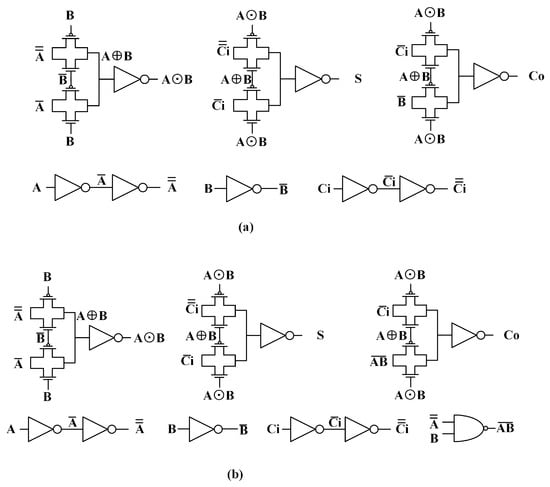
Figure 1.
PTL-based standard full adder cells: (a) Full adder from the TSMC 65 nm process; (b) full adder from the TSMC 40 nm process.
PTL circuits have a lower transistor count. However, the lower transistor count might not lead to a smaller area because PTL circuits have more complex connections. Fewer transistors with more connections might cause large wire loads and unexpected delays. Moreover, PTL-based cells might suffer from issues such as threshold loss [22,23], weak driving capacity [24], and uneven delay and power distribution. Circuits with PTL need to be properly designed to fully exploit their advantages.
In this paper, we propose a novel PTL full adder and a multiplier based on the proposed full adder. The main contributions of this paper are as follows:
- (1)
- A novel PTL full adder is proposed using two parallel PTL XOR gates to produce XOR and XNOR simultaneously, which reduces the parasitic capacitance on the critical path. The post-layout simulation shows a power improvement of 13.78% compared to conventional CMOS full adders.
- (2)
- We take a deep look at common issues with PTL-based adders, such as voltage loss, cascade delay, and glitch issues. Design principles regarding PTL circuits are concluded.
- (3)
- A multiplier based on the proposed full adder is designed. The post-layout simulation shows a power improvement of 8% compared to the multiplier produced by the Design Compiler synthesis tool.
The remainder of this paper is organized as follows: Section 2 reviews existing logic gates and full adders, including CMOS- and PTL-based adders. Section 3 presents our proposed full adder. Section 4 presents the multiplier based on the proposed full adder. Section 5 verifies the performance of our proposed multiplier. Finally, we conclude the paper in Section 6.
2. Existing Works
2.1. PTL Logic
PTL refers to a class of logic based on wired-OR logic. It uses pass transistors as controlled switches. A fundamental logic implemented by PTL is the XOR gate. It is also the basic component of full adders and multipliers.
There are references that present PTL XOR gates with various types of circuitry. Reference [24] presented a PTL XOR, as shown in Figure 2. It is composed of two pass gates, G0 and G1. When B = 0, G0 is turned on, and X = A. Otherwise, when B = 1, G0 is off, and X = Z (high impedance). When A = 0, the pass-transistor P0 from G1 is turned on, and Y = B. When A = 1, N0 is turned on, and Y = . For G0 alone, high impedance is not favorable for a logic gate. For G1 alone, threshold loss occurs when A = B. X and Y are shorted to produce S. G0 and G1 compensate for each other to solve the issue. The truth table is shown in Figure 1b.
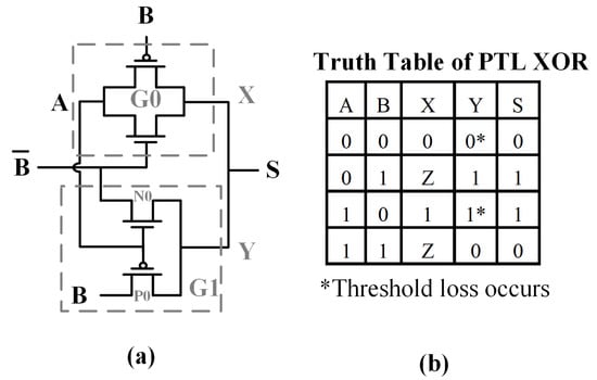
Figure 2.
PTL XOR proposed in 1992 [24]: (a) Circuit; (b) Truth Table.
Figure 3 shows a PTL XOR gate with only four transistors [25]. For each PMOS, the gate and source are connected to input ports “A” and “B”. This simplifies the circuitry but might suffer from a trade-off in threshold loss issues.
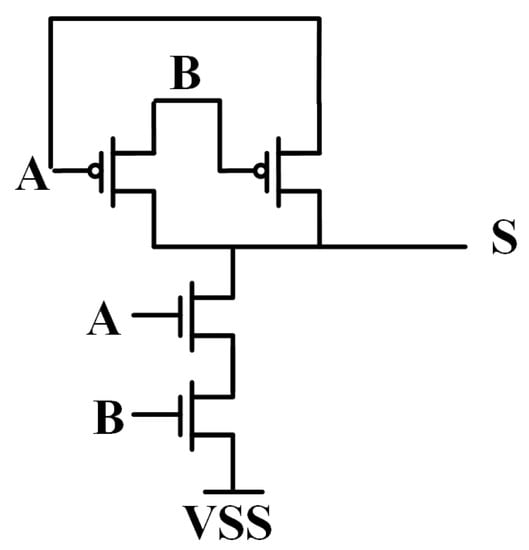
Figure 3.
PTL XOR proposed in 1998 [25].
Figure 4a,b show two XOR gates proposed in reference [26]. They are composed of 14 transistors and 6 transistors, respectively, including all inverters.
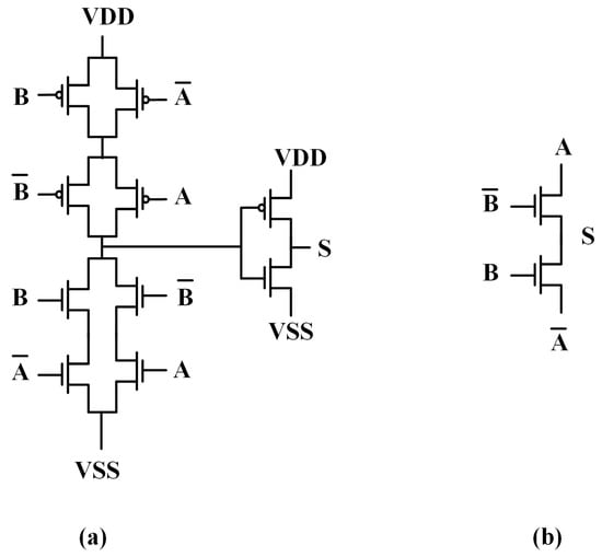
Figure 4.
PTL XOR proposed in 2020 [26]: (a) pass gate-based; (b) pass-transistor based.
Figure 5 shows the XOR gate from the TSMC 28 nm standard cell. It also includes a pass gate.
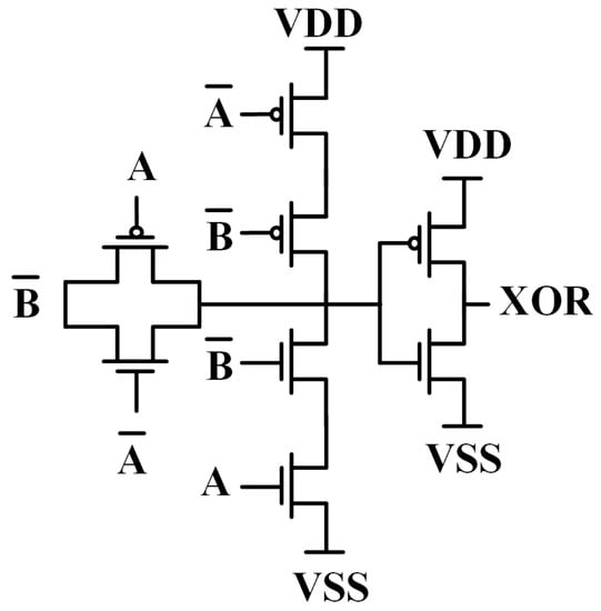
Figure 5.
XOR gate from the TSMC 28 nm standard cell.
Table 1 shows the delay and power consumption of all the XOR gates mentioned above. All circuits were modeled by the TSMC 28 nm process. The voltage of the power supply is 0.9 V. All circuits were modeled at the minimum size. The simulation was conducted on the Cadence platform. The input pattern included all 12 input flipping cases. The simulation testbench is shown in Figure 6.

Table 1.
Simulation of existing PTL-based XOR gates.
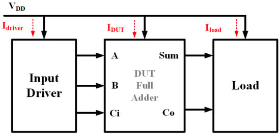
Figure 6.
The testbench of existing full adders.
In the table, the term “Power of DUT” denotes the power consumed by the full adder under the test alone (DUT refers to the device under test). The power of DUT is expressed as Equation (1).
“T” denotes the time for all 12 flipping cases. In this simulation, the frequency is 100 MHz.
However, it is not a sufficient method only estimating the power consumed by the DUT. The pass gates could directly conduct the voltage and current from the input driver. The PTL-based circuit might not only consume power on its own but could also contribute extra power to the input driver, as shown in Figure 7a. In addition, PTL circuits sometimes suffer from threshold loss issues as explained above, which might lead to extra power consumption in the load circuit, as shown in Figure 7b. To discuss the total power consumption of PTL-based circuits, it is fair to take the driver and the load into consideration. Therefore, in Table 1, the total power is listed as well. The total power is expressed as Equation (2).
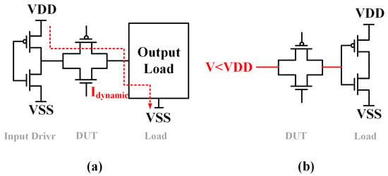
Figure 7.
Power consumption consideration of PTL-based circuits: (a) power estimation of the driver; (b) power estimation of the load.
As shown in Table 1, if we consider only the DUT alone, the XOR gate shown in Figure 3 (1998) consumes the least power. This is because there is no connection to the power rail in the 4T XOR circuit. However, it increases the power consumption of the driver circuit. Moreover, it suffers from a threshold loss issue, which means that when S = 0, the voltage is not 0 V but 133 mV. The XOR gate presented in Figure 4b has a threshold loss as well. When S = 1, the voltage is only 775 mV (VDD = 900 mV). The XOR gate presented in Figure 2a achieves the best performance.
2.2. Existing Full Adders
Figure 8 shows a typical circuit of a CMOS full adder. It consists of 28 transistors. We will call it the “28T” full adder. Many CMOS process libraries use this full adder circuit in their standard cells.
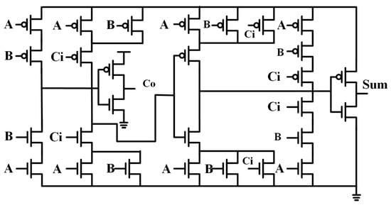
Figure 8.
A typical CMOS full adder circuit.
In 1992, a PTL full adder was proposed [24], as shown in Figure 9. It was composed of 16 transistors, including two PTL XOR gates and two pass gates acting as majority gates to produce the output carry, namely “Co”. In this paper, we call it “16T-1992”.
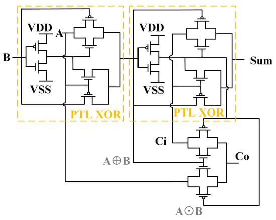
Figure 9.
The 16T full adder proposed in 1992 [24].
As shown in Figure 10, a full adder consisting of 14 transistors was proposed in 1996 [27]. It used the PTL XOR gates composed of only 4 transistors, as shown in Figure 3. We call it “14T-1996”.
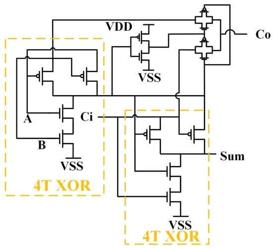
Figure 10.
The 14T full adder proposed in 1996 [27].
Figure 11 shows a full adder that was composed of only 10 transistors. It was proposed in 1999, and was referred to as the static energy-recovery full (SERF) adder [28]. It consisted of two four-transistor XOR gates. Moreover, it used NMOS and PMOS instead of two pass gates to perform the majority logic. It has been widely discussed because of its simple circuitry and threshold loss issue [29].
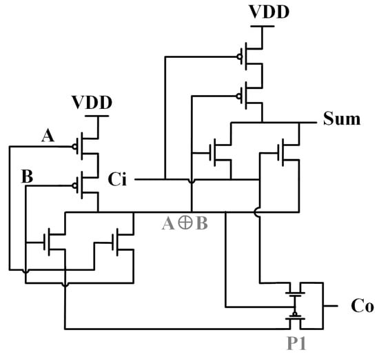
Figure 11.
“SERF” 10T full adder proposed in 1999 [28].
In 1999, a 14-transistor full adder was proposed [30], as shown in Figure 12. It only used six transistors to produce XOR and XNOR logic. We call it “14T-1999”. The transistors P0 and N0 compensated for the voltage loss when A = B.
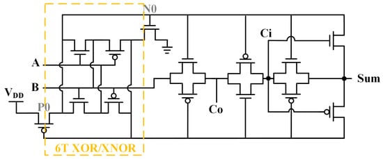
Figure 12.
The 14T full adder proposed in 1999 [30].
Figure 13 shows a full adder presented in 2019 [31]. It consists of 24 transistors, including all inverters.
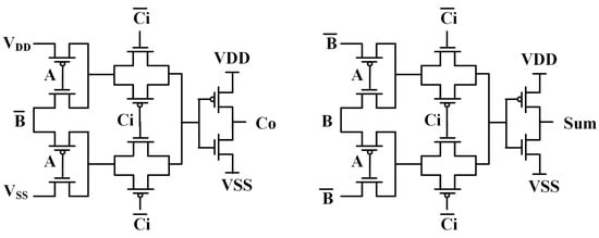
Figure 13.
The 24T full adder proposed in 2019 [31].
Table 2 shows the delay and power consumption of all the full adder circuits mentioned above. The simulation was conducted via the Cadence platform. All circuits were modeled by the 28 nm process. The size of all transistors was set to the minimum. The (A, B, Ci) input pattern included all 56 data-flipping cases.

Table 2.
Simulation of existing PTL full adders.
SERF 10T-1999 had a significant max delay value. Such a delay occurred when A = 0, C = 1, and B flipped from 1 to 0. In this case, the voltage at node “A ⊕ B” flipped from 1 to 0 but with a large delay, because the carrying capacity of PMOS “P0” decreased with the decrease of the A ⊕ B value. Moreover, this slow flipping further slowed down the flipping of another PMOS, “P1”. It caused a significant delay. Furthermore, 14T-1996 had a competitive delay performance. However, due to the voltage loss issue, the power of the DUT and the total power were high. Finally, 14T-1999 and 16T-1992 showed competitive performances compared to the two full adders mentioned above; 16T-1992 was better in both power and delay.
To further compare 28T and 16T-1992, the delays of all 56 cases are shown in Figure 14 and Figure 15.
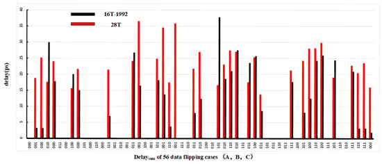
Figure 14.
Sum delay of 28T and 16T-1992.
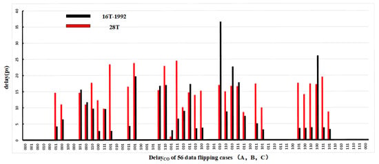
Figure 15.
Co delay of 28T and 16T-1992.
The maximum and average delays of the two types of full adders are listed in Table 3. As can be seen in the table, the sum delay of 16T-1992 is lower than 28T in most cases; however, in 5 out of 31 cases, 16T-1992 produced a sum slower than 28T CMOS FA; 3 of the 5 cases are related to B flipping, and 2 cases are related to A flipping.

Table 3.
The maximum and average delays of 28T and 16T-1992.
If we take a further look at the circuit of 16T-1992, as shown in Figure 16, we could see that when either A or B flips in an operation, the flipping always passes node “A ⊕ B”, which denotes the XOR logic results of A and B. This node connects to 10 transistors, which dramatically slow down the operation. In addition, the inverter encircled by the red frame is used to produce the XNOR results of A and B “A ⊙ B” from “A ⊕ B”. It contributes to a further propagation delay. If the connection of the “A ⊕ B” node could be reduced, the worst-case delay could be improved.
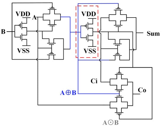
Figure 16.
The delay analysis of 16T-1992.
3. Proposed PTL Full Adder
3.1. Circuit Design
In this section, a novel PTL full adder is presented. The circuit of the proposed PTL full adder is shown in Figure 17. The novel proposed full adder consists of 18 transistors.
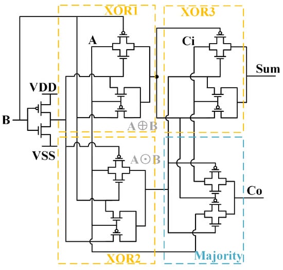
Figure 17.
The circuit of the proposed full adder.
Instead of using an inverter to produce XNOR from XOR, we used a parallel PTL XOR gate (“XOR2” conducting “”) to provide XNOR. As a result, the inverter was no longer needed. Similar to 16T-1996 and 14T-1996, we used two pass gates to form a majority gate to produce the output carry “Co”.
As the main reason for the large worst-case delay of 16T-1992 was the large parasitic capacitance at “A ⊕B”, by using a parallel PTL XOR gate, we distributed the connection count of “A ⊕B” to “A ⊙B”. The propagation path was, thus, split into two parallel paths, each with less parasitic capacitance. Theoretically, the “A ⊕B” and “A ⊙B” results arrived at the third PTL XOR gate, “XOR3”, or the PTL majority gate at the same time. Either path drives less load than 16T-1992.
Table 4 shows the parasitic capacitance of 16T-1992 and the proposed full adders. Both full adders are modeled with 28 nm process. The parasitic capacitance was extracted by the Calibre tool. The parasitic capacitance at the “A ⊕ B” node of the proposed 18T is 21% less than 16T-1992. The load capacitance is divided by the “A ⊙B” node. Since the two paths propagate parallelly, the worst-case delay could be reduced.

Table 4.
The parasitic capacitance of 16T-1992 and the proposed 18T full adders.
The worst-case delay could be further reduced by removing the inverter. Since there are fewer connections to the power rail, the power consumption of the proposed full adder is also reduced.
Table 5 shows the performance of the proposed full adder. The simulation was conducted on the Cadence platform. Due to the reduction of the inner load, the critical delay is improved. Moreover, the power consumption is also the smallest among the three types of full adders.

Table 5.
The performance of the proposed full adder.
However, the results shown in Table 4 might not necessarily suggest the true superiority of the proposed full adder. Since the inverter at the node “A ⊕ B” was removed, it lowered the driving capacity. It has more complex circuitry than 16T-1992, which might make the advantages shrink in a post-layout simulation.
Therefore, it is necessary to verify the post-layout performance to obtain more realistic characteristics of the proposed circuit.
We designed the layout of the proposed full adder, as well as the 16T-1992. The layout of the proposed full adder is shown in Figure 18. Figure 19 shows the layout of 16T-1992. Both layouts were designed based on a 28 nm CMOS process.
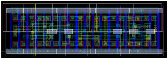
Figure 18.
Proposed full adder layout.
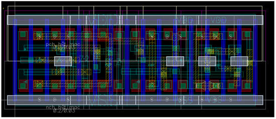
Figure 19.
16T-1992 layout.
Table 6 lists the post-simulation results. According to the table, the average delay of the three types of full adders is similar. The worst-case delay of the three types of adders increased. However, the delay of the two PTL-based adders increased more than that of the 28T adder, which turned the advantages of the delay into disadvantages. This suggests a stronger trend in PTL-based circuits, where power and delay tend to expand significantly if the parasitic parameter is considered.

Table 6.
The post-layout simulation results of the proposed full adder.
Moreover, our proposed adder and 16T-1992 adder have similar average delays to those of 28T but higher worst-case delays than 28T. This proves their uneven distribution.
Compared to 28T adder, a 13.78% power reduction could be obtained.
3.2. Analysis of Cascade Characteristics
A single PTL full adder has a delay similar to that of the 28T CMOS full adder. However, the delay of cascaded PTL-based adders increases exponentially. If we set up a PTL full adder chain, as shown in Figure 20, the delay of each adder is shown in Table 7.

Figure 20.
Cascaded PTL full adders.

Table 7.
The delay of cascaded full adders.
A dramatic increase in delay with cascade-level rises could be observed in the table. This is because the pass gate chain lacks a pull-up or pull-down transistor to provide drive. To model such a PTL-based adder chain, the pass gate chain could be simplified as an RC cascade, as shown in Figure 21. The delay of such a chain can be expressed as in (3). The term “n” denotes the cascade level.

Figure 21.
PTL full adders in cascade simplified by an RC chain.
Figure 22 shows the delay of each adder in cascade and the fit curve based on Equation (3). The factor “RC” could be estimated as in (4).
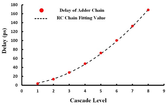
Figure 22.
Curve fitting of the delay of adders in cascade.
Therefore, it is not optimal to use too many PTL full adders in cascade, especially in multipliers that include adder arrays or adder trees. We could simply replace some 28T adders to break the PTL chain. If we consider an integer “m”, and replace a 28T with every m PTL full adder, the delay of the PTL-CMOS hybrid chain could be expressed as in (5).
The term denotes the Ci → Co delay difference between the 28T adder and the proposed PTL adder. Table 8 shows the post-layout simulation result of the Ci → Co delay of 28T and the proposed adder. The up arrow denotes the 0→1 flip of Ci, and the down arrow denotes the 1→0 flip of Ci. According to (5), “Delay (m)” could obtain a minimum value when , in other words, m = (2− 1. According to Table 8, we take (ps). Therefore, the optimal value of m is 2.08, which means that we could obtain the best speed for an adder chain of every two PTL adders and one 28T adder.

Table 8.
The post-layout simulation of the Ci → Co delay of 28T and the proposed adder.
3.3. Glitch Issue
Most PTL-based adders suffer from a glitch issue. Due to its weak driving capacity, the state of a pass gate is easily influenced by other inner flipping signals. It might be turned on unexpectedly and turned off immediately, thus forming a glitch. In most cases, the glitch might not lead to logic errors. But for the next-level circuits driven by the glitched adder, the dynamic power rises.
Table 9 shows the input flipping that causes glitches at output ports “Sum” and “Co”. Among all 56 cases, there are 13 cases with glitches. A total of 11 out of 13 cases are related to multi-input-flipping. This means that the proposed adder tends to cause glitch issues and increase the power of next-level circuits when more than one input flips.

Table 9.
Glitch issue of the proposed adder.
Therefore, to design a low-power multiplier, it is better to avoid having more than one input of the PTL full adder to flip at the same moment.
4. PTL-Based Multiplier
In this section, a low-power 8-bit signed multiplier based on the proposed adder is presented. Firstly, the key to optimizing the multiplication is to reduce the computation count. To achieve this purpose, carry-save array multipliers pass the carry to the next level adders, and Wallace tree methods compress the number of partial products in each level. Although Wallace tree methods have the most complex structure, they use the fewest adders.
Booth encoder methods [13], on the other hand, encode the input sequence according to a certain concept. An improved version of Booth encoding, known as modified Booth encoding (MBE), was proposed [14]. It enables parallel operations at higher radices. Table 10 illustrates the radix-4 MBE pattern, where the multiplicand is encoded in groups of 3 bits. The modified Booth encoder methods and Wallace tree combine to form the modified Booth Wallace tree (MBW) [13,32,33].

Table 10.
Radix-4 modified Booth encoding values [14].
In this design, we use the MBE and Wallace adder tree to reduce the circuitry. According to Table 10, the modified Booth encoder circuit could be implemented as shown in Figure 23. It produces partial products to the adder tree.
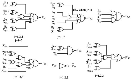
Figure 23.
The circuit of the modified booth encoder.
The adder tree for an 8-bit signed multiplier is shown in Figure 24. The adder tree consists of four rows, with each row composed of full adders and half adders. They compress the partial products in each row. After compression, the partial products are finally summed up by a series of carry-propagating adders.
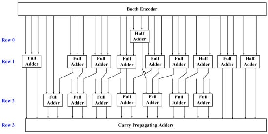
Figure 24.
The circuit of the adder tree.
According to Table 6, the proposed full adder has a 13.78% power advantage over the 28T CMOS full adder. This motivates the use of the proposed full adder in the adder tree to obtain the power advantage. As explained in Section 3.2, it is preferable to stagger the proposed adder and 28T adder both vertically and horizontally. In particular, in row 3, a minimum horizontally propagated delay could be obtained by staggering each proposed adder with one 28T adder. However, to pursue more low-power advantages, we decided to stagger one proposed adder and one 28T adder.
Moreover, as explained in Section 3.3, it is better to use the proposed adder, where three inputs flip at different moments. It is not optimal to use it in row 0 and row 1. Row 0 includes only a half adder. The inputs of adders in row 1 are mostly provided by the Booth encoder. It is reasonable to assume that the partial products arrive in row 1 at the same time. In this case, more than one input of an adder in row 1 would flip at the same time, leading to the glitch issue. Therefore, it is proper to put the proposed adders in row 2 and row 3. In row 2, the inputs of each adder are provided by different adders or the Booth encoder. We might assume different arrival moments for the propagation of each input flip. In row 3, the proposed adders and CMOS adders are staggered, as explained before. In row 0 and row 1, only CMOS half adders and full adders are used.
The final circuit of the adder tree is shown in Figure 25. It consists of 28 full adders and 3 half adders. Among the 28 full adders, 14 adders are the proposed adders. The rest of the full adders and half adders are CMOS-based.
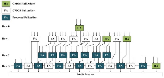
Figure 25.
The circuit of the proposed adder tree.
5. Simulation Results
In this section, the performance of the proposed multiplier is verified via post-layout simulation. The simulation was conducted on the Cadence platform. The multiplier was designed based on a 28 nm CMOS process. The typical power voltage was 0.9 V.
Firstly, we designed the layout of the proposed multiplier. We also used the Design Compiler (DC) synthesis tool to produce a multiplier for comparison, and we used the IC compiler to produce the layout of the synthesis multiplier. The layout is shown in Figure 26.
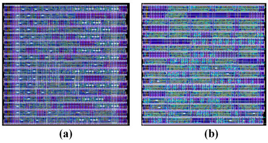
Figure 26.
The layout of multipliers: (a) proposed; (b) DC synthesis.
Figure 27 shows the post-layout simulation results of power consumption at multiple process corners. The red curve denotes the proposed multiplier, and the black curve denotes the synthesis multiplier. The simulation was conducted at room temperature at 27 °C. The simulation frequency was 500 MHz.
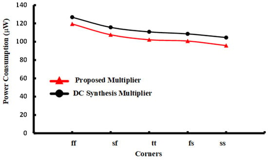
Figure 27.
Post-layout simulation of the power consumption.
For all corners, an 8% power reduction could be observed. The power reduction is mainly attributed to the power advantage from the proposed full adder.
Figure 28 shows the post-layout simulation results of the worst-case delay. A 6% delay increase could be observed. According to the post-layout simulation listed in Table 6, the proposed adder has a larger worst-case delay than the 28T full adder. The staggered carry-propagating adders in row 3 have delay advantages over the synthesis multiplier. The final 6% increase in the worst-case delay is the comprehensive result of delay optimization. It is the trade-off with the power advantage.
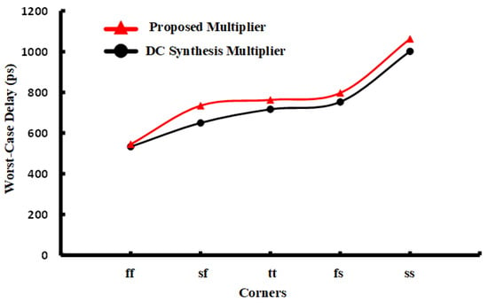
Figure 28.
Post-layout simulation of the worst-case delay.
Table 11 shows the comparison between our work and other multiplier studies. In the table, the term “PDP” denotes the product of power and delay, and the term “APP” denotes the product of power and area. We obtained the best PDP and ADP of all works. Admittedly, our work was based on the latest process. It might contribute to the performance advantages. Some of the work listed in the table was about the approximate multiplier design, which obtained better performance in delay and power compared to exact multipliers. Our work still maintained an advantage compared to approximate multipliers. The work “CSSP 2019 [34]” was based on the 32 nm process, which is close to our 28 nm process. Our work achieved only 19.02% of the PDP and 3.5% of the APP compared to “CSSP 2019”. This indicates the contribution of our work.

Table 11.
Comparison with other multiplier studies.
6. Conclusions
In this paper, we propose a novel PTL full adder circuit based on the 28 nm process. By using a parallel PTL XOR gate, we reduced the parasitic capacitance at the critical path of the adder and, thereby, reduced the worst-case delay. We also removed the inverter, which was to produce the XNOR result. Compared to a conventional CMOS-based full adder, the power consumption was reduced by 13.78%.
We also designed a low-power 8-bit signed multiplier based on the proposed full adder. The post-layout simulation showed an 8% power reduction compared to the multiplier produced by the DC synthesis tool. Compared to an 8-bit multiplier based on 32 nm presented in the references, our work achieved only 19.02% PDP and 3.5% APP of the reference.
Author Contributions
Circuit design of the full adder and multiplier, layout design for the full adder, simulation: N.Y.; circuit design, layout design, and post-layout simulation of the multiplier: W.P.; layout design of multiplier: Y.Y. and C.T.; supervision, project administration: Z.Y. All authors have read and agreed to the published version of the manuscript.
Funding
This work was supported in part by the Key-Area Research and Development Program of Guangdong Province under grants 2021B1101270005 and 2021B0101410004; in part by the National Key Research and Development Program of China under 2018YFB2202601; in part by the National Natural Science Foundation of China (NSFC) under grant 61834005 and grant 61902443; in part by the Guangdong Basic and Applied Basic Research Foundation under grant 2022A1515011708; in part by the Zhuhai Industry-Academic Collaboration program ZH22017001200097PWC.
Data Availability Statement
Due to privacy restrictions, research data in manuscripts cannot be disclosed.
Conflicts of Interest
The authors declare no conflict of interest.
References
- Pihl, J.; Aas, E.J. A Multiplier And Squarer Generator For High Performance Dsp Applications. In Proceedings of the IEEE Midwest Symposium on Circuits and Systems, Monterey, CA, USA, 3–6 November 1996. [Google Scholar]
- Hsu, S.; Venkatraman, V.; Mathew, S.; Kaul, H.; Anders, M.; Dighe, S.; Burleson, W.; Krishnamurthy, R. A 2GHz 13.6mW 12x9b Multiplier for Energy Efficient FFT Accelerators. In Proceedings of the European Solid-State Circuits Conference, Edinburgh, UK, 15–19 September 2008. [Google Scholar]
- Daryani, M.K.; Kumar, K. Implementation and Performance Evaluation of Parallel 8-point FFT using Vedic Multiplier. Int. J. Adv. Res. Electron. Commun. Eng. 2014, 3, 1783–1786. [Google Scholar]
- Sireesha, B. Modified Booth Multiplier with FIR Filter. Int. J. Sci. Res. 2014, 3, 798–802. [Google Scholar]
- Dempster, A.G.; Macleod, M. Use of minimum-adder multiplier blocks in FIR digital filters. IEEE Trans. Circuits Syst. II Analog. Digit. Signal Process. 1995, 42, 569–577. [Google Scholar] [CrossRef]
- Li, C.Y.; Chen, Y.H.; Chang, T.Y.; Chen, J.N. A Probabilistic Estimation Bias Circuit for Fixed-Width Booth Multiplier and Its DCT Applications. IEEE Trans. Circuits Syst. II Express Briefs 2011, 58, 215–219. [Google Scholar] [CrossRef]
- Masupe, S.; Arslan, T. Low Power VLSI Implementation of the DCT on Single Multiplier DSP Processors. VLSI Des. 2007, 11, 397–403. [Google Scholar] [CrossRef]
- Dempster, A.; Macleod, M. IIR digital filter design using minimum adder multiplier blocks. IEEE Trans. Circuits Syst. II Analog. Digit. Signal Process. 1998, 45, 761–763. [Google Scholar] [CrossRef]
- Parate, P.G.; Patil, P.S.; Subbaraman, S. ASIC Implementation of 4 Bit Multipliers. In Proceedings of the 2008 First International Conference on Emerging Trends in Engineering and Technology, Kobe, Japan, 18–20 November 2008; pp. 408–413. [Google Scholar] [CrossRef]
- Senthilpari, C.; Singh, A.K.; Diwakar, K. Low power and high speed 8 × 8 bit multiplier using non-clocked pass transistor logic. In Proceedings of the 2007 International Conference on Intelligent and Advanced Systems, Kuala Lumpur, Malaysia, 25–28 November 2007; pp. 1374–1378. [Google Scholar] [CrossRef]
- Barke, E. A Universal Pezaris Array Multiplier Generator for SRAM-Based FPGAs. In Proceedings of the IEEE International Conference on Computer Design: VLSI in Computers and Processors (ICCD’97), Austin, TX, USA, 12–15 October 1997. [Google Scholar]
- Hwang, K. Global and Modular Two’s Complement Cellular Array Multipliers. IEEE Trans. Comput. 1979, 28, 300–306. [Google Scholar]
- Booth, A.D. A signed binary multiplication technique. Q. J. Mech. Appl. Math. 1950, 4, 236–240. [Google Scholar] [CrossRef]
- Macsorley, O.L. High-Speed Arithmetic in Binary Computers. Proc. IRE 1961, 49, 67–91. [Google Scholar] [CrossRef]
- Goto, G.; Sato, T.; Nakajima, M.; Sukemura, T. A 54 * 54-b regularly structured tree multiplier. IEEE J. Solid-State Circuits 1992, 27, 1229–1236. [Google Scholar] [CrossRef]
- Gensuke, G. High Speed Digital Parallel Multiplier. U.S. Patent 5,465,226, 7 November 1995. [Google Scholar]
- Guild, H.H. Fully iterative fast array for binary multiplication and addition. Electron. Lett. 1969, 5, 263. [Google Scholar] [CrossRef]
- Yeo, K.S.; Roy, K. Low Voltage, Low Power VLSI Subsystems; McGraw-Hill Inc.: New York, NY, USA, 2005. [Google Scholar]
- Wu, X.; Prosser, F. Design of ternary CMOS circuits based on transmission function theory. Int. J. Electron. 1988, 65, 891–905. [Google Scholar] [CrossRef]
- Wu, X.W.; Prosser, F.P. CMOS ternary logic circuits. IEEE Proc. G—Circuits Devices Syst. 1990, 137, 21–27. [Google Scholar] [CrossRef]
- Wu, X. Theory of Transmission Switches and Its Application to Design of CMOS Digital Circuits. Int. J. Circuit Theory Appl. 2010, 20, 349–356. [Google Scholar] [CrossRef]
- Subramaniam, S.; Wilson, T.W.X.; Singh, A.K.; Murthy, G.R. A proposed reliable and power efficient 14T full adder circuit design. In Proceedings of the 2017 IEEE Region 10 Conference (TENCON 2017), Penang, Malaysia, 5–8 November 2017; pp. 45–48. [Google Scholar] [CrossRef]
- Vigneswaran, T.; Mukundhan, B.; Reddy, P.S. A Novel Low Power and High Performance 14 Transistor CMOS Full Adder Cell. J. Appl. Sci. 2006, 6, 1978–1981. [Google Scholar] [CrossRef]
- Zhuang, N.; Wu, H. A new design of the CMOS full adder. IEEE J. Solid-State Circuits 1992, 27, 840–844. [Google Scholar] [CrossRef]
- Shams, A.M.; Bayoumi, M.A. A New Full Adder Cell for Low-Power Applications. In Proceedings of the 8th Great Lakes Symposium on VLSI (GLS-VLSI’98), Lafayette, LA, USA, 19–24 February 1998; p. 45. [Google Scholar]
- Prasad, D.D. Design and Implementation of Full Adder using Different XOR Gates. Int. J. Innov. Technol. Explor. Eng. 2020, 9, 1422–1426. [Google Scholar] [CrossRef]
- Abu-Shama, E.; Elchouemi, A.; Sayed, S.; Bayoumi, M. An efficient low power basic cell for adders. In Proceedings of the 38th Midwest Symposium on Circuits and Systems, Rio de Janeiro, Brazil, 13–16 August 1995. [Google Scholar]
- Shalem, R.; John, E.; John, L.K. A novel low power energy recovery full adder cell. In Proceedings of the Symposium on VLSI, Kyoto, Japan, 17–19 June 1999. [Google Scholar]
- Amitha, M.; Deepa. Comparison between CMOS full adder and PTL full adder. IOP Conf. Ser. Mater. Sci. Eng. 2021, 1065, 012047. [Google Scholar] [CrossRef]
- Vesterbacka, M. 14-Transistor CMOS full adder with full voltage-swing nodes. In Proceedings of the IEEE Workshop on Signal Processing Systems (SiPS 99) Design and Implementation, Taipei, Taiwan, 20–22 October 1999. [Google Scholar]
- Hasan, M.; Saha, U.K.; Sorwar, A.; Dipto, M.A.Z.; Zaman, H.U. A Novel Hybrid Full Adder Based on Gate Diffusion Input Technique, Transmission Gate and Static CMOS Logic. In Proceedings of the IEEE 2019 10th International Conference on Computing, Communication and Networking Technologies (ICCCNT), Kanpur, India, 6–8 July 2019. [Google Scholar]
- Cooper, A.R. Parallel architecture modified Booth multiplier. IEE Proc. G (Electron. Circuits Syst.) 1988, 135, 125–128. [Google Scholar] [CrossRef]
- Fadavi-Ardekani, J. M*N Booth encoded multiplier generator using optimized Wallace trees. IEEE Trans. Very Large Scale Integr. Syst. 1993, 1, 120–125. [Google Scholar] [CrossRef]
- Boppana, N.; Kommareddy, J.; Ren, S. Low-Cost and High-Performance 8 × 8 Booth Multiplier. Circuits Syst. Signal Process. 2019, 38, 4357–4368. [Google Scholar] [CrossRef]
- Guo, Y.; Sun, H.; Kimura, S. Design of Power and Area Efficient Lower-Part-OR Approximate Multiplier. In Proceedings of the 2018 IEEE Region 10 Conference (TENCON 2018), Jeju Island, Republic of Korea, 28–31 October 2018. [Google Scholar]
- Venkatachalam, S.; Ko, S.B. Design of Power and Area Efficient Approximate Multipliers. IEEE Trans. Very Large Scale Integr. Syst. 2017, 25, 1782–1786. [Google Scholar] [CrossRef]
- Kumar, G.G.; Sahoo, S.K. Implementation of a high speed multiplier for high-performance and low power applications. In Proceedings of the 2015 19th International Symposium on VLSI Design and Test, Ahmedabad, India, 26–29 June 2015; pp. 1–4. [Google Scholar] [CrossRef]
Disclaimer/Publisher’s Note: The statements, opinions and data contained in all publications are solely those of the individual author(s) and contributor(s) and not of MDPI and/or the editor(s). MDPI and/or the editor(s) disclaim responsibility for any injury to people or property resulting from any ideas, methods, instructions or products referred to in the content. |
© 2023 by the authors. Licensee MDPI, Basel, Switzerland. This article is an open access article distributed under the terms and conditions of the Creative Commons Attribution (CC BY) license (https://creativecommons.org/licenses/by/4.0/).