Article

Capacitance Estimation for Electrical Capacitance Tomography Sensors Using Digital Processing of Time-Domain Voltage Response to Single-Pulse Excitation

by
Praveen Kalarickel Ramakrishnan
1,*,
Timothy Westwood
1,2,
Tomé Magalhães Gouveia
1,
Mahdi Taani
1,3,
Kylie de Jager
1,
Kenny Murdoch
1,
Andrey A. Orlov
4,
Mikhail S. Ozhgibesov
4,
Tatiana V. Propodalina
4 and
Natalia Wojtowicz
1
1
Zedsen Limited, 21a John St., London WC1N 2BF, UK
2
Barts and the London School of Medicine and Dentistry, Queen Mary University of London, London E1 4NS, UK
3
Department of Physics, King’s College London, London WC2R 2LS, UK
4
Perfect Art, 85 Great Portland St., 1st Floor, London W1W 7LT, UK
*
Author to whom correspondence should be addressed.
Electronics 2023, 12(15), 3242; https://doi.org/10.3390/electronics12153242
Submission received: 16 June 2023 / Revised: 17 July 2023 / Accepted: 24 July 2023 / Published: 27 July 2023
(This article belongs to the Special Issue Electromagnetic Applications in Industry and Medicine)

Abstract

:
In this paper, a new approach for capacitance measurement for electrical capacitance tomography (ECT) sensors is proposed. The method is based on the digital processing of the time-domain voltage measurements at the sensor electrodes. Furthermore, a robust capacitance estimation algorithm is developed to convert the measured voltage time-series to inter-electrode capacitances. The proposed measurement technique simplifies the electronic design of the ECT sensor and is suitable for use in applications requiring a compact device with a fast scan time. The accuracy and sensitivity of the method are investigated numerically and experimentally using a prototype sensor. In particular, the sensitivity of the estimated capacitance to measurement noise levels is analyzed in detail. Additionally, an analysis of the parameters that affect the accuracy of estimated capacitances is carried out from which we are able to demonstrate that the method is immune to effects such as stray capacitances between the electrodes and the ground. A prototype sensor with an open curved geometry on a millimeter scale is used to test the method empirically. Experimental results obtained for measurements with mineral oil and water are shown and compared against capacitances obtained using a physics-based forward model of the sensor. The inter-electrode capacitances in the range of tens of femtofarads to a few picofarads are estimated and a close match with the forward model results is obtained.

1. Introduction

Electrical capacitance tomography (ECT) is a measurement technique for determining the spatial distribution of the permittivity within a region using capacitance measurements taken on, or near, the surface of the region [1,2]. It is a non-invasive, low-cost imaging modality and has found applications in various fields [3,4]. An ECT sensing system is composed of the sensor electrodes near the region of interest (ROI), the sensing electronics for providing the excitation voltages and measuring the responses, and a computer for generating the images from the measured data [5].
The inter-electrode capacitances in typical ECT systems are very small and span a range from femtofarads to a few picofarads [6]. The measurement of the capacitances in this range can be challenging due to the sensitivity of the electronics required and the relatively large stray capacitances between the electrodes and ground, which exist in many applications. Despite these difficulties, a few methods have been proposed [7,8]. In particular, the charge–discharge and alternating current (AC) methods have been highly popularized due to being inherently immune to stray capacitances [5,9]. The charge–discharge method uses a square wave excitation to drive a current through the unknown capacitor. The current is then integrated using an operational-amplifier-based circuit to give a voltage proportional to the unknown capacitance value. In contrast, the AC method uses a sinusoidal excitation and subsequently demodulates the measured signal to obtain a voltage proportional to the unknown capacitance value. A number of modifications to these two fundamental measurement principles have been proposed [10,11,12].
The measurement techniques mentioned above are based on repeated cycles of charging and discharging the capacitor using either a series of pulses or sinusoidal excitation. However, there has been some work related to applying single-shot rectangular voltage as excitation for the capacitance measurement [13,14,15]. Unsurprisingly, the use of a single charge–discharge cycle increases the data acquisition rate required for many monitoring applications [8]. This approach has been used to design high-speed ECT systems, for example, in [13]. It is worth noting that the reconstruction of permittivity and conductivity is still possible when a single pulse is used. This was demonstrated in a numerical study carried out in [15]. However, one drawback of using a single-shot excitation is the increased impact of measurement noise affecting the signal-to-noise ratio (SNR). This shortcoming can be addressed by hardware modifications. In particular, the use of higher excitation voltages [14] or increasing the system gain [16] results in an increased SNR.
In this paper, we present a new approach that uses measured response voltages from a single-shot pulse excitation to digitally compute the unknown inter-electrode capacitances. Our approach has the advantage of requiring simpler hardware than other ECT systems, which require current integration via operational amplifiers to be performed. To the best of our knowledge, this is the first study of capacitance estimation for ECT applications using digital samples of measured voltage time-series. Similarly to other charge–discharge systems, which use a current integration approach, the proposed method is immune to the stray capacitances between the electrodes and the ground. However, the measurements can be affected by the parasitic capacitances of the printed circuit board (PCB) connecting lines, which could be reduced by careful design and measurement calibration.
A possible application of the proposed method is in medical imaging. It could be used to design an inexpensive, non-ionising, lightweight hand-held device to perform fast scans, and the processing could be performed offline. Like other single-pulse-based methods, we obtain the average response of the material in a range of frequencies. The method could also be extended to extract information at multiple frequencies using further processing of the time-series voltage data, enabling frequency-dependent imaging of the permittivity distribution. This is particularly important for imaging biological tissues and other complex materials with frequency-dependent permittivity values.
The proposed method is tested with a prototype sensor board that has an open curved geometry. We provide both a numerical analysis of the method as well as demonstrate the method using experimental results. The sensor is modeled and solved using the finite element method (FEM) [17] to generate the numerical results. The sensitivity of the estimated capacitances to noise is studied using simulated data. The first experimental results are provided for a prototype sensor and compared against the capacitances computed using the forward solver.
This paper is organized as follows. In Section 2, an overview of the ECT system is provided followed by details of the prototype sensor board, its equivalent circuit representation, the capacitance estimation algorithm, and the forward model to generate numerical data. In Section 3, the main results obtained are discussed, which include the voltages obtained from the forward simulation, the reconstructed capacitances using simulated data, the sensitivity of the results to noise, the experimental results using the measured data, and a comparison with existing ECT systems. The conclusions of this paper are provided in Section 4.

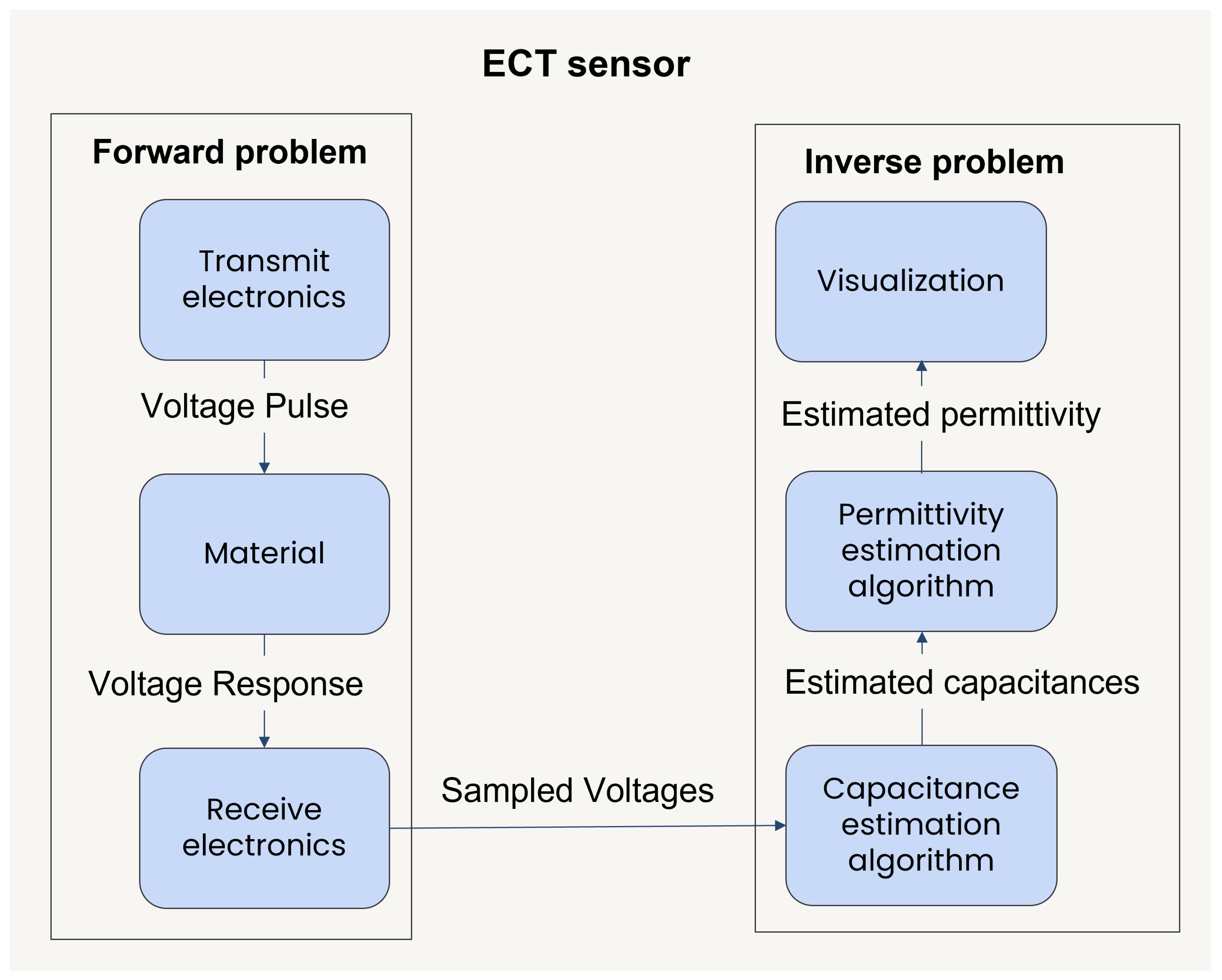
2. Materials and Methods

A block diagram describing the working of the prototype time-domain ECT sensor is shown in Figure 1. The sensor is composed of an array of parallel electrodes and the material to be imaged is placed near it. A single pulse is applied to excite one electrode at a time and the responses of all the electrodes are recorded. The problem of determining the response voltages based on the input voltage at the transmit electrode for a given sensor geometry and material in the ROI is known as the forward problem. In contrast, the inverse problem consists of using the measured response voltages to obtain a reconstructed estimate of the permittivity of the material in the ROI. In our system, the reconstruction of the permittivity map consists of two main steps. In the first step, the sampled time-domain voltages are digitally processed to estimate the capacitances between the pairs of electrodes in the sensor. In the second step, the permittivity distribution is reconstructed using the estimated capacitances. In this paper, we describe the capacitance estimation algorithm and analyze its performance. A detailed description and analysis of the permittivity estimation algorithm is out of the scope of this paper, but some of the commonly used techniques can be found in the literature [18,19,20].
In an ECT system, the forward model is used in the inverse solver to compute the cost function for a given material permittivity distribution. This cost function is minimized to estimate the permittivity values. In our case, a model of the forward problem is also useful to synthetically generate the voltage data to test the capacitance estimation algorithm for a known setup. This enables us to study the accuracy, sensitivity, and stability of the algorithm using simulated data. The modeling of the forward problem involves two parts [21]. The first part is the formulation of a partial differential equation (PDE) that arises from the electroquasistatic model of the fields in the material and the second is the construction of the ordinary differential equation (ODE) that models the circuit dynamics. The solution of the PDE with simple boundary conditions can be used to compute the capacitances for the given geometry and material properties. The coupled PDE-ODE system is associated with the time-domain voltage solution.
The main focus of this paper is the capacitance estimation algorithm that converts the voltage measurements into inter-electrode capacitances. The algorithm developed is general enough to accommodate different shapes of the excitation pulse. The proposed algorithm is based on an equivalent circuit representation of the system. This representation is also useful for the voltage computation and can be exploited to generate synthetic data for testing the capacitance estimation algorithm.
In the subsections that follow, we provide details on the prototype sensor board, its equivalent circuit representation, the algorithm for capacitance estimation, and the forward model.

2.1. Prototype Sensor Board

The prototype sensor board used to test the proposed method is shown in Figure 2. There are N E = 15 electrodes on a PCB, numbered E 1 , E 2 , , E 15 . The electrodes are 6 mm wide, 69 μ m thick, and 146 mm long and are separated by a distance of 10 mm. The PCB shape is flexible and is supported by a 3D printed frame made of plastic material (nylon polyamide 12) and defines a curved geometry with a radius of curvature of 71 mm at the top of the board. The board is 1.6 mm thick, and the frame extends 8.4 mm below the board. A ground plate is attached at the bottom of the frame, which is 10 mm below the electrodes. The material to be imaged is placed above the electrodes.
A square pulse of low bandwidth (<1 MHz) is used as the time-domain excitation voltage and a multiplexer applies the input pulse sequentially to each electrode. The multiplexer establishes a connection between the selected electrode and the signal generator before the pulse is applied so that the transient effects of the multiplexer do not affect the signals. One end of each electrode is connected to the multiplexer through a 10 k Ω series resistance. On the other end, 1 M Ω pull-down resistances are used to form the receive nodes, which are then fed to an analog-to-digital converter (ADC) via buffer amplifiers. In our experimental setup, an oscilloscope is used to serve the functions of ADC and the associated memory.

2.2. Equivalent Circuit Representation of the Sensor

The proposed capacitance estimation algorithm is based on an equivalent circuit representation of the sensor. The material to be imaged is assumed to be non-conductive and the considered signals are of low enough frequencies for electroquasistatic approximation to be valid. Therefore, the inter-electrode impedance can be modeled as capacitances, while the resistance and inductance effects can be neglected. The electrode to ground capacitances arise out of multiple factors that include the capacitances of the multiplexer and buffer amplifiers, stray capacitances influenced by the material on the sensor, and additional variable factors. As will be seen later, the capacitance estimation algorithm does not depend on knowing the value of the stray capacitances to the ground and hence they can be included in the model as an unknown quantity. Moreover, the value of the electrode to ground capacitances can be assumed to generate the synthetic data to test the estimated capacitances.
Figure 3 represents the equivalent circuit of the sensor, shown here for a three-electrode system for simplicity. The nodes that represent each electrode E i , i = 1 , 2 , , N E are called the K-nodes, denoted K i , with the associated voltages V K , i . These K-nodes are in turn connected to the pull-down resistance R K G , i . The components C K G , i represent the net capacitances to the ground on the receive side and include unknown stray capacitances. Together, they form the resistance–capacitance (RC) receive circuit, and the voltage across them is fed to the oscilloscope via buffer amplifiers. On the opposite end, the electrodes are connected to the source via the multiplexer, represented here by the switches S i , through series resistances, denoted as R T K , i , and the corresponding nodes are called the T-nodes, denoted as T i . The resistances and the net capacitances from T-nodes to the ground are represented by R T G , i and C T G , i . The value of C T G , i is also influenced by unknown factors and hence can be considered as stray. The capacitances C i , j denote the inter-electrode capacitances between E i and E j , which carry the information about the permittivity distribution of the material placed near the sensor. The source voltage V S has a resistance R S and produces an input pulse, which is applied sequentially to each electrode using the multiplexer. For each transmit pulse, the voltages at the T-node, V T , i , and at the K-node, V K , i , are measured for each electrode.

2.3. Capacitance Estimation

The inter-electrode capacitances C i , j are usually measured using a current integrating circuit, which outputs a voltage proportional to the unknown value. Here, we discuss an alternative approach that uses a capacitance estimation algorithm based on a simple voltage time-series measurement scheme. For single-pulse excitation applied to each electrode, the voltages at both T-nodes and K-nodes are measured for all the electrodes. The measurements are then processed digitally to estimate the capacitances.
At any K-node of the equivalent circuit, the Kirchoff’s Current Law (KCL) can be written for any instant of time t n as
V T , i ( t n ) V K , i ( t n ) R T K , i = C K G , i d V K , i ( t n ) d t + V K , i ( t n ) R K G , i + j C i , j d V K , i ( t n ) d t d V K , j ( t n ) d t
Using (1) and considering the source voltage applied sequentially to each electrode, the system of simultaneous differential equations for the nodal voltages at any instant of time can be written as
[ K ] d [ V K ( t n ) ] d t = [ L ] [ V K ( t n ) ] + [ M ] [ V T ( t n ) ] ,
where,
[ K ] = C K G , 1 + j 1 C 1 , j C 1 , 2 C 1 , N E C 2 , 1 C K G , 2 + j 2 C 2 , j C 2 , N E C N E , 1 C N E , 2 C K G , N E + j N E C N E , j ,
[ L ] = 1 R K G , 1 + 1 R T K , 1 0 0 0 1 R K G , 2 + 1 R T K , 2 0 0 0 1 R K G , N E + 1 R T K , N E ,
[ M ] = 1 R T K , 1 0 0 0 1 R T K , 2 0 0 0 1 R T K , N E .
[ V K ( t n ) ] and [ V T ( t n ) ] are N E × N E matrices whose j t h columns represent the instantaneous K-node and T-node voltages, respectively, when the source voltage is applied to the electrode E j . In other words, [ V K ( t n ) ] i , j = V K , i ( t n ) and [ V T ( t n ) ] i , j = V T , i ( t n ) when switch S j in Figure 3 is closed. The numeric values of [ V K ( t n ) ] and [ V T ( t n ) ] in (2) are measured at N T discrete instants of time for a given sampling rate. The resistances in the circuit are known and therefore [ L ] and [ M ] matrices are readily available. The matrix [ K ] is composed of the unknown capacitances, which need to be estimated.
A couple of approaches could be adopted to solve for the capacitances using (2) given the time-series voltage data. One possibility is to employ a least squares approach to minimize the total error for the N T time instants. This can be performed by repeating (2) N T times with the voltage values at each instant, forming an over-determined system of size N E 2 × N T . However, this would require an estimate of the numerical derivative of the time-series K-node voltages, d [ V K ] d t , which is error-prone in the presence of measurement noise.
We use the integrated version of (2), avoiding the need for computing numerical derivatives of the data, to estimate the capacitances more reliably. Therefore, for a time window between the instants T w 1 and T w 2 , the integrated version of the equation becomes
[ K ] [ Δ V K ] = [ L ] [ V K i n t ] + [ M ] [ V T i n t ] .
Here, [ Δ V K ] i , j = V K , i ( T w 2 ) V K , i ( T w 1 ) forms the matrix of voltage differences in the time window with E j as the excited electrode. The matrices [ V K i n t ] and [ V T i n t ] are defined by the numerical integrals of the voltages in the time window with the elements [ V K i n t ] i , j = T w 1 T w 2 V K , i and [ V T i n t ] i , j = T w 1 T w 2 V T , i , with E j excited.
The resulting Equation (6) forms a linear algebraic system of size N E 2 , which can be solved to obtain the [ K ] matrix. This can be performed by taking the transpose of (6) and inverting the square matrix [ Δ V K ] T to obtain
[ K ] = [ K ] T = [ Δ V K ] T 1 [ L ] [ V K i n t ] + [ M ] [ V T i n t ] T .
The required inverse of the matrix in (7) can be computed with an LU-decomposition-based algorithm implemented in standard numerical libraries [22]. The numerical solution obtained with this procedure, [ K ] s o l , could have slight asymmetry due to measurement and computational errors, which can be adjusted by taking the symmetric part [ K ] = [ K ] s o l + [ K ] s o l T 2 . The inter-electrode capacitances, C i , j , are then easily deduced from [ K ] using (3).
It is worth noting that, by having the measurements of both T-node and K-node voltages, we obviate the need to know accurate values of parameters like C T G , i , R T G , i , and R S for the computation. This insulates the capacitance estimation algorithm from errors due to uncertainty in those parameters, which is the rationale for measuring V T , i in addition to V S and V K , i . Moreover, since the derived linear system treats C K G , i as an additional unknown, the method is immune to stray capacitances to the ground. However, the estimated values can still be affected by other error sources, such as parasitic capacitances of the lead wires, that appear parallel to the inter-electrode capacitances in the equivalent circuit, which needs to be minimized via good PCB design and measurement calibration. The effect of these parasitic capacitances can be larger for ECT systems with larger spatial separation between the electrodes and the hardware, but the method can still be applicable with adequate compensation. If the buffer amplifiers can be placed close to the electrodes, the length of subsequent connection lines to the data capture circuitry will have a minimal effect on the measurement parasitics. In addition, the error is linearly related to the differences in the resistance values R K G , i i and R T K , i , which can be controlled by selecting components of low tolerances and temperature drift. The choice of the integration window ( T w 1 and T w 2 ) can also affect the estimated capacitances, which is explored in Section 3.4.
We also note that, although a prototype sensor with a simple geometry is used to test the method, the equivalent circuit and the capacitance estimation algorithm described here are more general and applicable to sensors with more complex geometries and different length scales. In particular, the same measurement technique is also applicable in the case of sensors with non-uniform electrodes having irregular shapes.

2.4. Forward Model

Now we consider a physics-based forward model of the sensor board. As mentioned before, the forward model is used for the numerical computation of capacitances and voltages. Apart from its use in the inverse solver, it will be exploited to generate the simulated data for testing the capacitance estimation algorithm. At sufficiently low frequencies (<1 MHz) and for the length scales involved (mm), the electromagnetic fields around the sensor can be modeled using an electroquasistatic approximation. By assuming that all the non-metallic materials in the computational domain Ω are linear and non-conductive, the electric potential u ( t , x ) , as a function of the position x and time t, satisfies [21]
· ε 0 ε r u ( t , x ) = 0   i n   Ω , u ( t , x ) = V K , i ( t )   o n   E i , u ( t , x ) = 0   o n   G j , ε 0 ε r u ( t , x ) · n ^ = 0   o n   Ω C ,
where E i , i = 1 , 2 , N E are the electrode surfaces, G j , j = 1 , 2 , N G are the surfaces of the ground plates within the region, and Ω C = Ω i E i j G j is the outer boundary of the domain. The constant ε 0 is the permittivity of free space and ε r is the relative permittivity distribution in the region. Note that (8) depends on time only through the time dependence of the boundary voltages V K , i ( t ) on the electrode surfaces. In a DC setting, with the ith electrode excited to a constant voltage V K , i and the remaining electrodes grounded ( V K , j = 0 for j i ), the inter-electrode capacitance can be computed using
C i , j = 1 V K , i E j ε 0 ε r u · n ^   d s ,
where u solves (8).
A similar equation can be used to compute the capacitance between the electrode i and the ground plates, C G , i , where the charge needs to be calculated on the surface of all the ground plates in the system. For known electrode potentials, the PDE in (8) can be solved numerically using the FEM. We thus have a method to compute the inter-electrode capacitances, C i , j , for a given geometry and material permittivity ε r , m a t e r i a l . The total capacitances to the ground are parallel combinations of C G , i with other stray capacitances present in the system.
One way to compute the time-domain voltages is by solving a coupled PDE-ODE system [21]. This is performed by combining the electroquasistatic Equation (8) with the ODE arising out of the circuit analysis. These two are then coupled through the charge/current flowing across the electrode boundary. However, we note that the capacitances C i , j between the electrode pairs are dependent only on the solution of the PDE through (9) and are independent of the circuit dynamics. Therefore, the voltage computation can be decoupled by first solving the PDE and computing the inter-electrode capacitances, which are then used in the equivalent circuit shown in Figure 3. The voltage computation then reduces to the solution of this circuit and can be carried out using a standard circuit-simulation software such as SPICE [23].

3. Results and Discussion

In this section, we provide the results obtained using the proposed method for the prototype sensor. The generation of time-domain voltage data using the forward solver is described first. Following this, the estimated capacitances from the simulated voltage data are presented, which are compared with the true values. Next, the sensitivity of the algorithm to measurement noise is analyzed. After that, the effects of integration time window and denoising filter and the immunity of the method to stray capacitances are discussed. Finally, results with experimentally measured data and comparison with existing ECT systems are provided.

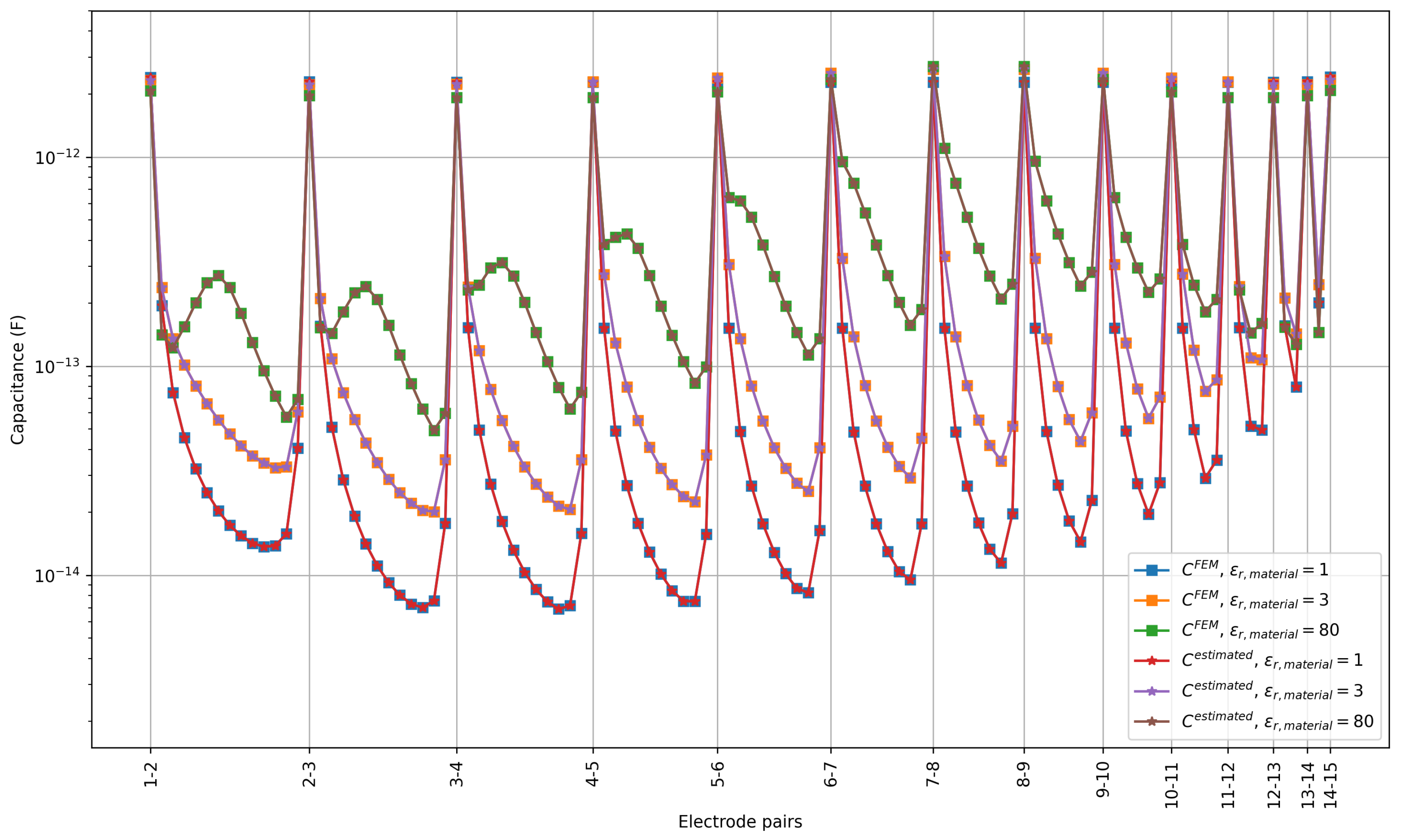
3.1. Forward Simulation

As described before, the prototype sensor is made up of N E = 15 electrodes, each having a length of 146 mm. For a material placed above the sensor that has cylindrical symmetry, the geometry of the sensor allows for a 2D modeling of the problem. In this case, only the cross-sectional plane perpendicular to the length of the electrodes needs to be modeled.
The geometry creation, meshing, and FEM solution were carried out using the open-source finite element software FreeFem++ [24]. A first-order nodal element scheme was used for the FEM solution. The 2D geometry used for the FEM simulation is shown in Figure 4. The computational domain is of a 375 mm width and 250 mm height. The extended parts of the board on the left and the right accommodate the electronic components and the signal ground. The relative permittivity of the board is ε r , b o a r d = 4 and that of the frame is ε r , f r a m e = 3 . A representational material with a circular cylindrical geometry and of relative permittivity ε r , m a t e r i a l = 2 is shown on the sensor with a gap of 1 mm between the central electrode and the material. For the FEM simulation, the region near the electrodes was meshed more finely to improve the accuracy of the solution. The actual size of the mesh was chosen based on a mesh convergence analysis.
The FEM simulation was carried out to obtain the inter-electrode capacitances, C i , j F E M . These capacitances were then used to generate the voltages by solving the SPICE model of the equivalent circuit. The K-node voltages obtained after solving the time-domain forward problem when the electrode E 1 was excited are shown in Figure 5. The results are shown for the material permittivity ε r , m a t e r i a l = 1 , which corresponds to air. The source voltage V S is a single square pulse of 20 μ s duration with a rise time of 50 ns. The circuit parameters used for the simulation were R S = 10   k Ω , R T K , i = 10   k Ω , R K G , i = 1   M Ω , C T G , i = 1 pF, and C K G , i = 1 pF, and R T G , i was not connected.

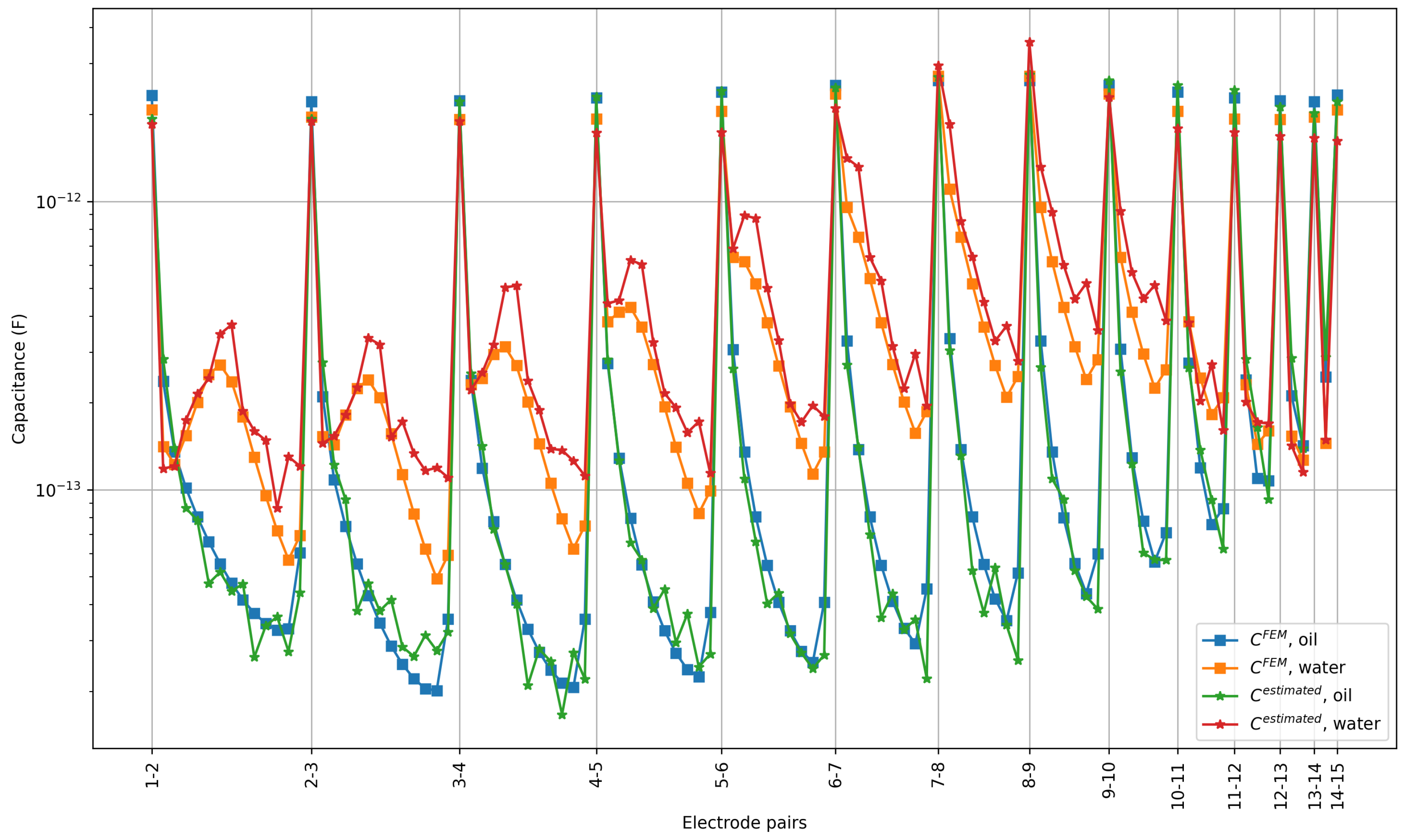
3.2. Estimated Capacitances Using the Algorithm

The results obtained for the simulated voltages were used to validate the capacitance estimation algorithm. The voltages for each excitation electrode were generated and the linear system in (6) was solved to obtain the estimated capacitances C i , j e s t i m a t e d . The required numerical integration was carried out using the trapezoidal rule. The voltages were generated with a sampling time of 0.4 ns and the values on an interval from 0 to 1 μ s were used for the estimation. Figure 6 shows the capacitances obtained for three different permittivity values, ε r , m a t e r i a l = 1 , 3 and 80, which correspond to typical values for air, oil and water, respectively [25]. The estimated capacitances are very close to the true capacitances from the FEM simulation and they are coinciding in the figure. The relative difference between the estimated and true capacitances is defined as
η C , i , j = | C i , j e s t i m a t e d C i , j F E M | C i , j F E M .
These errors are shown in Figure 7. It can be observed that the capacitance estimation algorithm reconstructs the true capacitances from given voltages very accurately. The relative errors are less than 10 6 for all electrode pairs and for all the permittivity values considered.

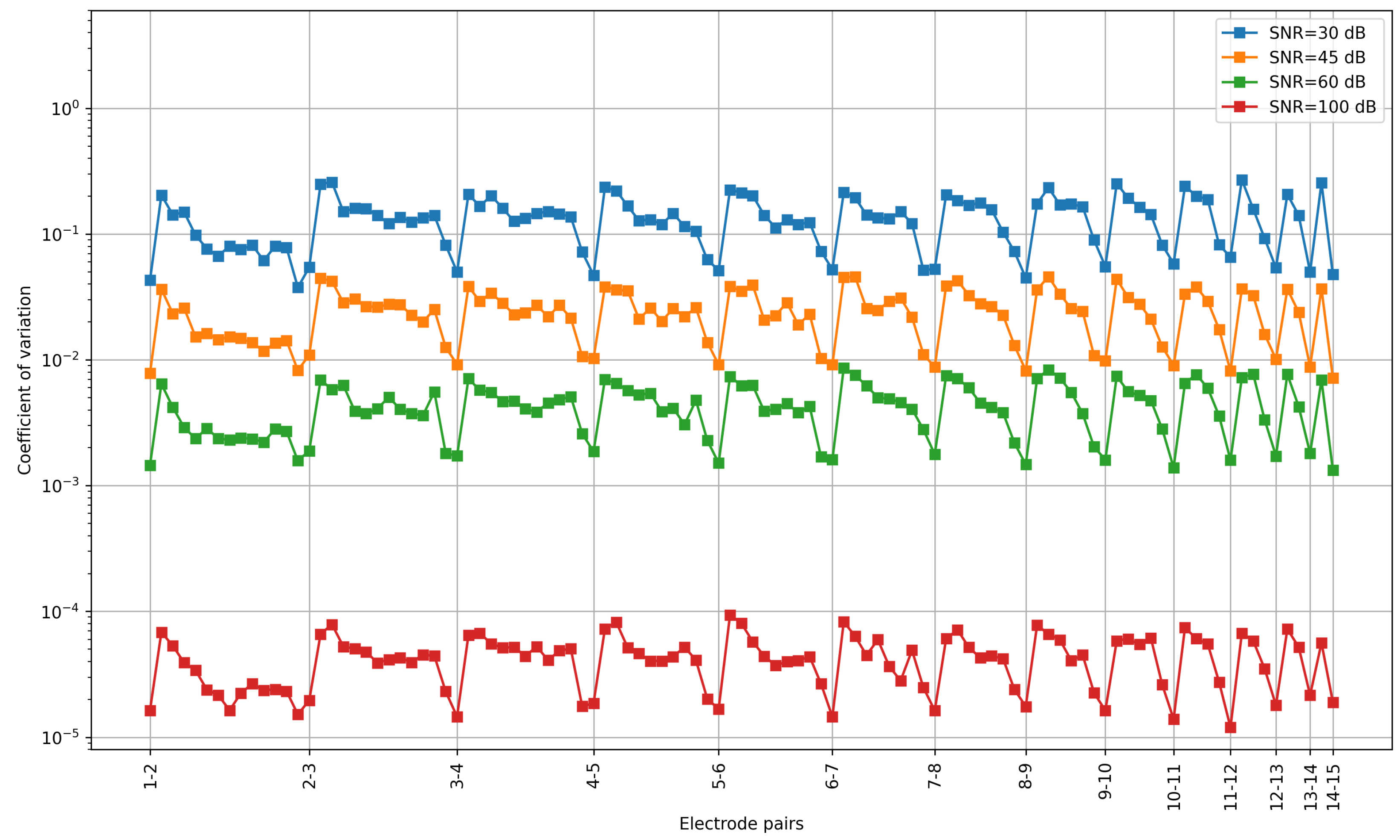
3.3. Sensitivity to Noise

The results in the previous subsection were obtained with simulated voltages computed using known capacitance values. Now, we study the sensitivity of the capacitance estimation algorithm when Gaussian noise is added to the voltage values. The uncertainty in the estimates can be quantified using the coefficient of variation defined as the ratio of the standard deviation to the mean of the estimated capacitances [14]. The uncertainty for each electrode pair for different SNR levels is shown in Figure 8, which was computed using 30 realizations of the noisy signals.
Figure 9 shows the relative differences between estimated and true capacitances for different SNR levels with the material permittivity set to that of air. For high SNR values, the capacitances are very close to the true value from the FEM solution. However, when the noise level increases, the errors in the estimated capacitances become larger.
Figure 10 shows the convergence of the estimated capacitances with respect to SNR levels. The variation in the maximum of the relative capacitance errors over all electrode pairs, i.e.,
η C , m a x = m a x i , j ( η C , i , j ) ,
is plotted against SNR levels for different material permittivities. For example, for ε r , m a t e r i a l = 80, the relative error reduces from around 60% for S N R = 25 to 10% for S N R = 40 and is below 1% for S N R = 60 . Similar results can be observed for other permittivity values. Therefore, we can say that the capacitance estimation algorithm gives reasonable results when the noise level is not too high. Next, we look at the parameters that can influence the accuracy of the estimation in the presence of noise.

3.4. Effect of Integration Time Window

One of the parameters that can be chosen for the capacitance estimation is the time window in which the data are processed. Figure 11 shows the results for window sizes defined by different end times, T w 2 , with the fixed start time T w 1 = 0 . The results are shown for the material permittivity, ε r , m a t e r i a l , set to air permittivity. The linear system in (6) involves the calculation of the numerical integrals, V K , i i n t and V T , i i n t , and the voltages difference over the interval, Δ V K , i . The integrals have a smoothing effect and taking a larger interval improves the accuracy of the calculation by averaging out the noise over the integration window. As for the voltage difference terms, Δ V K , i , the accuracy also improves on larger intervals, as long as the voltages are rising, i.e., before the peak levels are reached. Therefore, in general, we expect that the accuracy improves with larger T w 2 , but the improvement tapers off and can even worsen after the voltages have decayed down to a low value compared to the noise levels (see Figure 5). This can be confirmed by the results in Figure 11, where the maximum errors decrease when the time window increases from T w 2 = 0.1   μ s to 5 μ s but then increase for T w 2 of 10 μ s and 20 μ s . Therefore, the time window should be selected based on the expected time constants of the voltage decay curves. It should be large enough so that the noise can be averaged out by the integrals but not so large that the voltage differences in the window become too small.

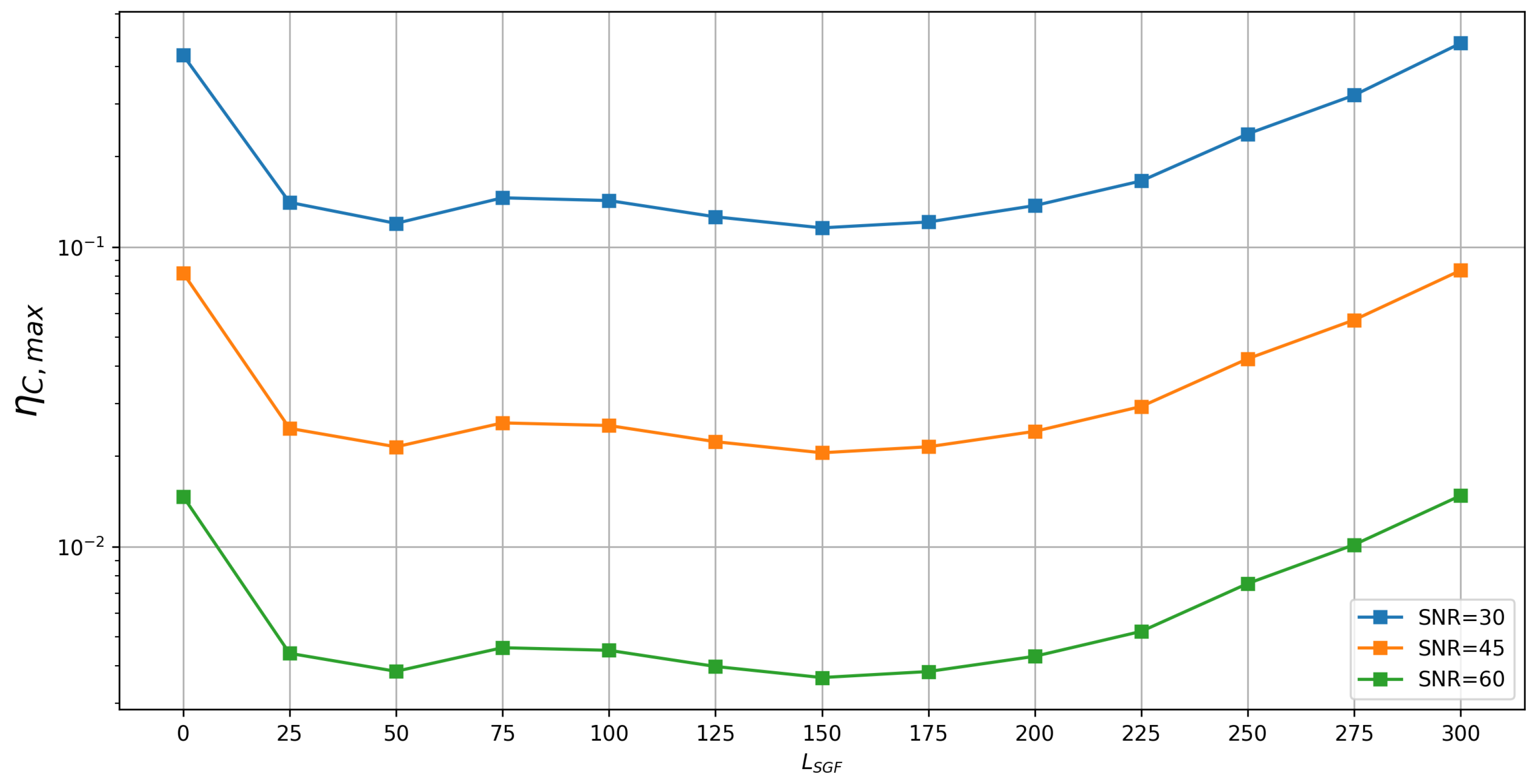
3.5. Effect of Denoising Filter

We have seen that the capacitance estimation works well provided the signal-to-noise ratio levels are not too low. In cases where the SNR is small, the use of denoising filters can be advantageous. An option is to use the well-known Savitzky–Golay filter, which smooths the signal by using the least squares method to fit consecutive windows of data points with a low-degree polynomial [26]. Here, we use a first-order Savitzky–Golay filter of a chosen length, L S G F . Figure 12 shows η C , m a x vs. filter length for different SNR levels for ε r , m a t e r i a l = 1 . The case in which filter the is not applied is denoted by L S G F = 0 . It can be seen that there is a large reduction in the errors when the filter is applied. The error decreases with the filter length initially. After some point, increasing the filter length is not beneficial any more, as it can start affecting the actual information about the variation in the signal. For example, with S N R = 45 dB, the maximum capacitance error η C , m a x is 8.2% if the filter is not applied. It reduces to 2.5% when L S G F = 25 , which corresponds to a time window of 1 ns, since the sampling time is 0.4 ns. The error reduces further to 2.1% when L S G F = 50 , after which it goes back up again and reaches 8.3% when L S G F = 300 . In summary, oversampling the voltages enables the application of the denoising filter without affecting the signal, thus improving the SNR.

3.6. Effect of Stray Capacitances

In ECT systems, the stray capacitances can be much larger than the measured capacitances and can have values higher than 100 pF [5]. As mentioned before, the developed algorithm is resistant to the effects of stray capacitances between the electrodes and the ground. This is because in Equation (2), and consequently in Equation (6), these capacitances are considered as unknowns and the currents flowing through them are accounted for. In Figure 13, we provide a numerical demonstration of this effect. The simulation is carried out for air by considering equal K-node to ground capacitance values, C K G , for all electrodes, which are varied in the range of 25 pF to 200 pF. A time window from 0 to 5 μ s is used for capacitance estimation. It can be observed that the maximum relative error in the inter-electrode capacitances remains stable over the wide range of stray capacitances. For instance, in the case of SNR = 40 dB the errors vary in the range of 5.87% to 6.36%, and for SNR = 60 dB the variation is between 0.57% and 0.62%. Thus, we can confirm that the stray capacitances do not have a large effect on the estimated capacitances.

3.7. Results with Measured Data

Now, we present the experimental results obtained using the voltage measurements from the board. Two materials, mineral oil and water, were used for the measurements. Both the materials were enclosed in a cylindrical bottle with a diameter of 116 mm. The bottle was made of plastic with a wall thickness of less than 0.5 mm and was placed on the electrodes. Voltage pulses of 5 V amplitude, 50 μ s rise time, and 20 μ s duration were applied to the sensor. The voltages obtained from 30 repeated measurements were averaged to improve the SNR seen by the capacitance estimation algorithm. Figure 14 shows the capacitances estimated using the measured voltages on the sensor board. The results from the FEM simulation are also shown, which were obtained using mineral oil and water permittivities of 3 and 80, respectively [25]. The thickness of the plastic wall of the bottle was neglected in the FEM model and a gap of 1 mm was considered between the top of the electrodes and the phantom.
It can be seen that the estimated capacitances are close to the capacitances computed using the FEM model. We obtain capacitances in the range of tens of femtofarads to a few picofarads. The total relative difference in capacitances,
η C , L 2 = i , j i | C i , j e s t i m a t e d C i , j F E M | 2 i ( C i , j F E M ) 2 ,
i , j = 1 , 2 , , N E = 15 , is 7.22% in the case of oil and 22.49% in the case of water. The ECT imaging systems usually minimize L2 capacitance differences to reconstruct the permittivity values [18]. The pattern of the capacitance values for different electrode pairs is very similar for both C i , j F E M and C i , j e s t i m a t e d .
It is worth remembering that the absolute capacitances are not always critical in ECT imaging as calibration is usually used to compensate for the differences [6,20,27]. Calibration is needed to adjust for the errors introduced due to offset capacitances, which can be time-dependent in some applications. The choice and analysis of the calibration procedure to be followed depends on the application domain and the requirements of the imaging algorithm and a detailed discussion is out of the scope of this paper.
The observed differences are a combination of errors in the estimated capacitances and the uncertainties in the forward model. The capacitance estimation algorithm can be affected by factors such as parasitic capacitances of the lead wires and lower SNR levels for voltage signals. As mentioned before, the parasitic capacitances appear parallel to the inter-electrode capacitances, causing the estimated capacitances to be higher. The SNR of voltage signals can become worse for electrodes that are far from the excited electrode, especially for sensors with open geometry. The SNR levels of the individual signals were estimated using denoised signals as references, which were obtained by first filtering and then averaging them over the repeated measurements [14]. For the measured signals, we obtained SNR levels above 55 dB for close electrode pairs, but they were below 20 dB for farther electrode pairs in a few cases. These capacitances between farther electrode pairs tend to be of smaller magnitudes as well, making them more difficult to estimate.
The FEM solution used for the comparison also has some modeling errors associated with it, due to the uncertainty in the parameters used in the simulation. The dimensions and the positions of the electrodes, the board, and the material all have tolerances that can affect the results of the forward solver. As mentioned, the geometry of the bottle containing the materials was also simplified in the simulation by ignoring the plastic wall thickness. Any distortion to the shape caused due to the weight of the material was also ignored. The permittivity values of the material also have tolerances associated with them. A simplified homogeneous model of the multilayered PCB was used. The discretization errors in the FEM solution also contribute to the observed differences.
Given the various sources of differences, we can say that the FEM simulation and the proposed algorithm independently produce similar capacitances. The developed algorithm could be used in ECT imaging with suitable calibration to adjust for the differences with the forward solver capacitances. Therefore, these results provide the experimental validation of the proposed capacitance measurement technique for ECT applications.

3.8. Comparison with Existing ECT Systems

The preliminary results from the early prototype sensor were used to demonstrate the novel capacitance measurement technique. In this subsection, we assess the performance indicators achievable with our proposed method and compare them with state-of-the-art devices commonly employed in the field. As mentioned before, most of the existing devices are based on the charge–discharge method [28] and AC method, while single-pulse methods have also been discussed in the literature. While existing ECT systems are primarily designed for real-time imaging applications [8], our proposed method is specifically tailored to applications that necessitate rapid scanning followed by offline image reconstruction.
The hardware requirements for the new method are much lower than those for traditional ECT methods. The circuits for the AC method are highly complex as precision AC signals need to be generated and signal demodulation needs to be performed. The charge–discharge method requires a circuit of medium complexity as the charge switching across the capacitors of interest needs to be timed. The circuit complexity required for the proposed method is lower than the other methods since the underlying principle is a simple RC circuit excited by a single pulse. The computational complexity of the capacitance estimation is related linearly to the number of voltage samples used for processing. This calculation can be performed offline to minimize the scanning time.
The typical measurement duration of conventional ECT systems is summarized in Table 1 in [14]. In general, single-pulse methods yield significantly faster measurements compared to AC and charge–discharge methods, which involve voltage averaging over multiple cycles. In our prototype device, we operated at a low multiplexer switching frequency, utilizing a 40 μ s data acquisition window for each electrode pair. The actual measurement speed depends on the chosen operating frequency. It is possible to design the device to operate at higher frequencies to achieve higher measurement speeds. This would require adjustments to the time constant of the RC receive circuit and the bandwidth of the buffer amplifiers in the measurement circuit, ensuring that voltage decay occurs sufficiently before the subsequent pulse is applied. At any frequency, further improvement in acquisition speed can also be achieved by concurrently reading all the receive electrode voltages for any excited electrode. Importantly, it should be emphasized that our proposed method necessitates a larger amount of data storage and transfer, as all voltage samples need to be transmitted for capacitance estimation. Therefore, it is crucial to have sufficient storage and data transfer rates for the ADC so that the measurement speed is not impeded.
The typical SNR levels for existing ECT systems are also given in [14]. In this case, the variations of charge–discharge and AC methods use average voltages over multiple cycles to improve the SNR. Therefore, there is a trade-off between the measurement duration and precision. Higher input voltage levels may also be used to improve the SNR [14], at the cost of increased circuit complexity. The typical SNR levels observed for our prototype sensor were around 56 dB at 2 pF and 18 dB at 19 pF for 30 repeats. However, the SNR of the oversampled voltages can be improved by digital filtering as described before. Therefore, there is also a trade-off between the SNR levels achieved by digital filtering and the quantity of the data to be transferred. It is worth noting that increasing the operating frequency by reducing the RC time constant will also reduce the measured voltage levels and consequently result in a worse SNR. In summary, the measurement speed, SNR levels, and storage requirements can be optimized for our prototype sensor subject to the trade-offs discussed and can be studied in more detail as part of future work.

4. Conclusions

In this work, a novel approach to measure the capacitances for ECT sensors based on the digital processing of time-domain voltages was described and analyzed. The method uses the voltage response to single-pulse excitation to estimate the inter-electrode capacitances. This approach simplifies the hardware design and reduces the power and space requirements of the device. The sensitivity of the method to noisy voltages was studied in detail using numerical simulations. Furthermore, we demonstrated that digital filtering can be used to increase the SNR of the signal and improve the accuracy of the capacitance estimation. We also showed that increasing the integration window can improve the accuracy of the estimated capacitances provided there are sufficient differences between voltages at the start and the end of the window. We also demonstrated that our method is inherently immune to stray capacitances to the ground but can be affected by parasitic capacitances of lead wire connecting the electrodes.
The capacitance algorithm was also applied to experimentally collected data. With oil and water as the materials, capacitances ranging from tens of femtofarads to a few picofarads were extracted from voltage data. We demonstrated that these values were in good agreement with simulated values obtained using the FEM solution of the forward model. The results indicate that, with suitable calibration, the method can have possible applications in ECT imaging. The digital processing of the time-series voltages can possibly be extended to extract the information at multiple frequencies, which is critical for biological tissues and other materials with frequency-dependent permittivity values.

Author Contributions

Conceptualization, P.K.R.; Methodology, P.K.R., M.T., A.A.O., M.S.O. and T.V.P.; Software, P.K.R., T.M.G. and M.T.; Validation, P.K.R., T.W., T.M.G., K.d.J., A.A.O. and M.S.O.; Formal analysis, P.K.R. and M.T.; Investigation, P.K.R., M.T., K.d.J., K.M. and T.V.P.; Resources, K.d.J. and K.M.; Data curation, T.M.G. and M.T.; Writing—original draft, P.K.R.; Writing—review & editing, P.K.R., T.W., T.M.G., A.A.O., M.S.O., T.V.P. and N.W.; Visualization, P.K.R.; Supervision, N.W.; Project administration, N.W. All authors have read and agreed to the published version of the manuscript.

Funding

This research received no external funding.

Data Availability Statement

The data presented in this study are available on request from the corresponding author. The data are not publicly available due the need to protect commercial interests of Zedsen Limited.

Conflicts of Interest

All authors at the time the research was conducted were either employed by Zedsen Limited or engaged with Zedsen in a commercial capacity.

References

  1. Huang, S.; Plaskowski, A.; Xie, C.; Beck, M. Tomographic imaging of two-component flow using capacitance sensors. J. Phys. E Sci. Instrum. 1989, 22, 173. [Google Scholar] [CrossRef]
  2. Marashdeh, Q.; Fan, L.S.; Du, B.; Warsito, W. Electrical capacitance tomography—A perspective. Ind. Eng. Chem. Res. 2008, 47, 3708–3719. [Google Scholar] [CrossRef]
  3. Rasel, R.K.; Chowdhury, S.M.; Marashdeh, Q.M.; Teixeira, F.L. Review of Selected Advances in Electrical Capacitance Volume Tomography for Multiphase Flow Monitoring. Energies 2022, 15, 5285. [Google Scholar] [CrossRef]
  4. Wang, H.; Yang, W. Application of electrical capacitance tomography in circulating fluidised beds—A review. Appl. Therm. Eng. 2020, 176, 115311. [Google Scholar]
  5. Yang, W.Q. Hardware design of electrical capacitance tomography systems. Meas. Sci. Technol. 1996, 7, 225. [Google Scholar]
  6. Yang, W. Design of electrical capacitance tomography sensors. Meas. Sci. Technol. 2010, 21, 042001. [Google Scholar] [CrossRef]
  7. Huang, S.M.; Stott, A.L.; Green, R.G.; Beck, M.S. Electronic transducers for industrial measurement of low value capacitances. J. Phys. E Sci. Instrum. 1988, 21, 242. [Google Scholar]
  8. Saied, I.; Meribout, M. Electronic hardware design of electrical capacitance tomography systems. Philos. Trans. R. Soc. A Math. Phys. Eng. Sci. 2016, 374, 20150331. [Google Scholar] [CrossRef]
  9. Huang, S.; Xie, C.; Beck, M.; Thorn, R.; Snowden, D. Design of sensor electronics for electrical capacitance tomography. IEE Proc. G Circuits Devices Syst. 1992, 139, 83–88. [Google Scholar] [CrossRef] [Green Version]
  10. Marashdeh, Q.; Warsito, W.; Fan, L.S.; Teixeira, F.L. A multimodal tomography system based on ECT sensors. IEEE Sens. J. 2007, 7, 426–433. [Google Scholar] [CrossRef]
  11. Hu, X.; Katsouros, M.; Yang, W.; Huang, S. Further analysis of charge/discharge capacitance measuring circuit used with tomography systems. Sens. Transducers J. 2007, 80, 1246–1256. [Google Scholar]
  12. Sun, S.; Cao, Z.; Huang, A.; Xu, L.; Yang, W. A high-speed digital electrical capacitance tomography system combining digital recursive demodulation and parallel capacitance measurement. IEEE Sens. J. 2017, 17, 6690–6698. [Google Scholar]
  13. Wang, B.; Ji, H.; Huang, Z.; Li, H. A high-speed data acquisition system for ECT based on the differential sampling method. IEEE Sens. J. 2005, 5, 308–312. [Google Scholar]
  14. Smolik, W.; Kryszyn, J.; Radzik, B.; Stosio, M.; Wróblewski, P.; Wanta, D.; Olszewski, T.; Szabatin, R. Single-shot high-voltage circuit for electrical capacitance tomography. Meas. Sci. Technol. 2016, 28, 025902. [Google Scholar] [CrossRef]
  15. Wanta, D.; Makowiecka, O.; Smolik, W.T.; Kryszyn, J.; Domański, G.; Midura, M.; Wróblewski, P. Numerical evaluation of complex capacitance measurement using pulse excitation in electrical capacitance tomography. Electronics 2022, 11, 1864. [Google Scholar] [CrossRef]
  16. Kryszyn, J.; Wanta, D.M.; Smolik, W.T. Gain adjustment for signal-to-noise ratio improvement in electrical capacitance tomography system EVT4. IEEE Sens. J. 2017, 17, 8107–8116. [Google Scholar]
  17. Jin, J.M. The Finite Element Method in Electromagnetics; John Wiley & Sons: Hoboken, NJ, USA, 2015. [Google Scholar]
  18. Yang, W.; Peng, L. Image reconstruction algorithms for electrical capacitance tomography. Meas. Sci. Technol. 2002, 14, R1. [Google Scholar] [CrossRef]
  19. Smolik, W.T.; Radomski, D. Performance evaluation of an iterative image reconstruction algorithm with sensitivity matrix updating based on real measurements for electrical capacitance tomography. Meas. Sci. Technol. 2009, 20, 115502. [Google Scholar] [CrossRef]
  20. Cui, Z.; Wang, Q.; Xue, Q.; Fan, W.; Zhang, L.; Cao, Z.; Sun, B.; Wang, H.; Yang, W. A review on image reconstruction algorithms for electrical capacitance/resistance tomography. Sens. Rev. 2016, 36, 429–445. [Google Scholar] [CrossRef]
  21. Westwood, T.J. PDE Based Models of Electric Field Sensors and Their Corresponding Inverse Problems. Ph.D. Thesis, University of Oxford, Oxford, UK, 2020. [Google Scholar]
  22. Anderson, E.; Bai, Z.; Bischof, C.; Blackford, S.; Demmel, J.; Dongarra, J.; Du Croz, J.; Greenbaum, A.; Hammarling, S.; McKenney, A.; et al. LAPACK Users’ Guide, 3rd ed.; Society for Industrial and Applied Mathematics: Philadelphia, PA, USA, 1999. [Google Scholar]
  23. Vogt, H.; Hendrix, M.; Nenzi, P.; Warning, D. Ngspice Users Manual Version 40 plus. 2023. Available online: https://ngspice.sourceforge.io/docs/ngspice-manual.pdf (accessed on 22 July 2023).
  24. Hecht, F. New development in FreeFem++. J. Numer. Math. 2012, 20, 251–266. [Google Scholar] [CrossRef] [Green Version]
  25. Jakoby, B.; Vellekoop, M.J. Physical sensors for water-in-oil emulsions. Sens. Actuators A Phys. 2004, 110, 28–32. [Google Scholar] [CrossRef]
  26. Press, W.H.; Teukolsky, S.A. Savitzky-Golay smoothing filters. Comput. Phys. 1990, 4, 669–672. [Google Scholar] [CrossRef]
  27. Yang, W. Calibration of capacitance tomography systems: A new method for setting system measurement range. Meas. Sci. Technol. 1996, 7, L863. [Google Scholar]
  28. Process Tomography Ltd. Electrical Capacitance Tomography System. Type TFLR 5000. Operating Manual Issue. 2009, Volume 1. Available online: http://www.tomography.com/pdf/Fundamentals%20of%20ECT.pdf (accessed on 22 July 2023).
Figure 1. A block diagram of the prototype ECT sensor. A material is placed near the sensor, a single voltage pulse is applied to each electrode, and the response voltages are measured at all the electrodes. The measured voltages are digitally processed to obtain the capacitances, which are in turn used to create an image representing the permittivity distribution of the material.
Electronics 12 03242 g001
Figure 2. Photograph of the experimental setup with the sensor board of curved geometry connected to the signal generator and oscilloscope is shown on the left. The view of the board from below, showing the frame, the ground plate, and the electronics is shown on the right.
Electronics 12 03242 g002
Figure 3. Equivalent circuit representing a sensor with three electrodes. The capacitances C 1 , 2 , C 2 , 3 , and C 1 , 3 are the inter-electrode capacitances. Additionally, C T G , i and C K G , i for i = 1 , 2 , 3 are influenced by the unknown stray capacitance in the system.
Electronics 12 03242 g003
Figure 4. The 2D geometry simulated by the FEM solver. The sensor PCB has a relative permittivity of 4 and is supported by the frame with a relative permittivity of 3. A cylindrical material with a relative permittivity of 2 is shown on top of the sensor, and the background is air with a relative permittivity of 1.
Electronics 12 03242 g004
Figure 5. The voltages on the K-node electrodes when the pulse input is applied to electrode E 1 .
Electronics 12 03242 g005
Figure 6. Plot of true and estimated capacitances for three different material permittivities. The true capacitances were computed with the FEM solver and were then used to obtain the voltage data for the capacitance estimation algorithm. The x-axis represents all 105 unique electrode pairs 1-2, 1-3, …, 2-3, 2-4, …, 14-15, some of which are not explicitly labeled to avoid clutter.
Electronics 12 03242 g006
Figure 7. Plot of relative errors in estimated capacitances for three different material permittivities. The true capacitances were computed with the FEM solver and were then used to obtain the voltage data for the capacitance estimation algorithm. The x-axis represents all 105 unique electrode pairs 1-2, 1-3, …, 2-3, 2-4, …, 14-15, some of which are not explicitly labeled to avoid clutter.
Electronics 12 03242 g007
Figure 8. The coefficient of variation of the estimated capacitances for different SNR levels. The results are shown for four different SNR levels and the material permittivity set to that of air. The x-axis represents all 105 unique electrode pairs 1-2, 1-3, …, 2-3, 2-4, …, 14-15, some of which are not explicitly labeled to avoid clutter.
Electronics 12 03242 g008
Figure 9. The relative errors in estimated capacitances for different SNR levels. The results are shown for four different SNR levels and the material permittivity set to that of air. The x-axis represents all 105 unique electrode pairs 1-2, 1-3, …, 2-3, 2-4, …, 14-15, some of which are not explicitly labeled to avoid clutter.
Electronics 12 03242 g009
Figure 10. Convergence of the maximum relative capacitance errors, η C , m a x , with the SNR levels for different material permittivities.
Electronics 12 03242 g010
Figure 11. Plot of maximum relative capacitance error, η C , m a x , vs. SNR for different integration time windows specified by T w 2 with T w 1 = 0 . The results were obtained with the material permittivity ε r , m a t e r i a l = 1 .
Electronics 12 03242 g011
Figure 12. Plot of maximum relative capacitance error, η C , m a x , vs. the length of the Savitzky–Golay filter, for different SNR levels. The results were obtained with the material permittivity ε r , m a t e r i a l = 1 and an integration time window defined by T w 2 = 1 μ s. The case in which the filter is not applied is denoted by L S G F = 0 .
Electronics 12 03242 g012
Figure 13. Plot of maximum relative capacitance error, η C , m a x , vs. K-node to ground capacitance for different SNR levels. The capacitances, C K G , i , are taken as the same value, C K G , for each electrode, i = 1 , 2 , 15 , and are varied from 25 pF to 200 pF. The results were obtained with the material permittivity ε r , m a t e r i a l = 1 and an integration time window defined by T w 2 = 5 μ s.
Electronics 12 03242 g013
Figure 14. Plot of capacitances obtained from measured data with cylindrical phantoms for two different materials: oil and water. The results are compared against the value obtained from the FEM simulation using the oil and water permittivity values of 3 and 80, respectively. The x-axis represents all 105 unique electrode pairs 1-2, 1-3, …, 2-3, 2-4, …, 14-15, some of which are not explicitly labeled to avoid clutter.
Electronics 12 03242 g014
Disclaimer/Publisher’s Note: The statements, opinions and data contained in all publications are solely those of the individual author(s) and contributor(s) and not of MDPI and/or the editor(s). MDPI and/or the editor(s) disclaim responsibility for any injury to people or property resulting from any ideas, methods, instructions or products referred to in the content.

