1. Introduction
Since Dawon Kahng at Bell Laboratories created the first MOSFET in 1960, silicon-based MOSFETs have been employed as power devices [
1]. Germanium (Ge) was utilized to create solid-state devices in the 1950s, but due to the small band gap (0.6 eV), these devices could only work at temperatures under 100 °C due to large leakage current at high temperatures [
2]. As a result of silicon’s 1.12 eV band gap and 1500 cm
2/Vs electron mobility, devices can function at 200 °C [
3]. Si has been the material of choice for the bulk of power devices for nearly five decades. The energy gap, electron mobility, thermal conductivity and electric field of Si as a material may become a restraining parameter in the near future. Incomplete body diode reverse recovery is another major issue with Si and SiC MOSFETs. The power MOSFET’s partial body diode reverse recovery for the LLC resonant converter topology presents a possible system reliability concern [
4]. Super junction technology in Si devices has nullified these restrictions to some extent [
5,
6].
Wide-bandgap (WBG) devices, such as SiC MOSFETs and GaN HEMTs, have recently attracted a lot of interest in the design of power electronics systems [
7]. Wide-bandgap (WBG) devices have far quicker turn-on/off times, almost nil reverse recovery loss and significantly lower conduction losses than typical Si MOSFETs or insulated-gate bipolar transistors (IGBTs) [
8]. In comparison to silicon, GaN has a substantially larger 1000 cm
2/Vs electron mobility and band gap of 3.4 eV [
9]. Due to the lack of an inherent body diode, GaN devices are better suited for use in high-frequency applications. In comparison to Si MOSFET, they also demand less drive power, which lowers drive losses. Higher-frequency operation enables highly efficient and more compact converters by lowering the size of resonant converter passive components, or in other words, by minimizing the size of magnetics [
10]. Devices made of GaN also have a very small on-resistance for a specific breakdown voltage than Si devices. The device’s on-resistance (
) has inverse relation to both the third power of the energy gap
and the electron mobility
[
11,
12].
For a given breakdown voltage, the on-resistance of a GaN HEMT will be nearly 15 times lower than that of a Si MOSFET. As a result, the converter’s efficiency will increase by lowering conduction losses in the switches. On the other hand, GaN HEMTs have substantially lower output capacitance (Coss) and gate charge (Qg) than silicon MOSFETs, which leads to quicker on/off times and lower driving loss [
13].
The switch-mode power supply was designed to operate at higher frequencies due to the recent need for high energy density, which is an unavoidable trend in the development of power electronics [
14]. High-frequency, however, also entails high electromagnetic interference (EMI) pollution and high switching energy consumption [
15,
16]. Therefore, in the most recent few years, researchers from all over the world have been interested in resonant converters due to their soft-switching operation and high-frequency characteristic [
17]. These converters are widely used in LCD TV power supplies, LED lighting drivers, EV charging stations, photovoltaic systems and for other useful products due to their advantages of high energy density and efficiency, magnetic integration, electrical isolation, low harmonic pollution and electromagnetic interference, wide output ranges, and low voltage stress [
18]. The LLC resonant converters has combined benefits of all others resonant converters, containing DC isolation, reliable no-load operation, low needs of current ripples of capacitor filter, advantages in the voltage regulation of resonant current, soft-switching range [
19].
On the other hand, ZVS at main side of power switches and ZCS at secondary side of rectifier diodes are used to run the LLC resonant converters. Therefore, these converters can attain high efficiency and low switching losses. Since these converters are frequency-controlled converters, the load characteristics and switching frequency have a significant impact on their output voltage. However, the optimal design of the reactive components is unaffected by the variable frequency control [
20]. The power flow in these resonant converters is adjusted by shifting the converter’s switching frequency below or above resonant frequency of resonant tank. Switching of resonant converters at zero current or zero voltage is possible [
21,
22].
Single-stage resonant converters with PFC were presented in [
23,
24,
25] to minimize the drawback of Si MOSFET. In [
23,
24], a power factor corrected (PFC) converter is proposed with the application of resonant converter topology, and then it is applied to an LED driver [
25], resulting in power supplies with greater efficiency and reduced profile. However, the switches work at asymmetrical duty ratio in these articles, which compromises the best power factor performance and complicates the driving and control circuits by adding 3rd harmonics to input current. The viability of LLC resonant topology functioning as a power factor correction converter with 50 percent duty cycle switch operation has been demonstrated in [
26]. The viability of the LLC topology functioning as a PFC converter with 50% duty cycle switch operation is demonstrated in [
26]. The authors of [
27] presented an interleaved parallel LLC resonant converter. The circuit architecture is more complex and has a small operating frequency range. In [
28], an LLC resonant converter with a three-bridge arm has been presented. It is a hybrid of two complete bridges with the addition of two auxiliary switches on the secondary side. The authors of [
18] presented a low-voltage LLC resonant converter. The whole input range is split into two parts: a high input voltage range and a low input voltage range. However, there is yet no simple LLC resonant converter design that provides good power factor correction with high efficiency and high power density. Therefore, for resonant soft-switching topologies which are working at high frequency like the LLC resonant converter, GaN HEMTs demonstrate considerable benefits over silicon MOSFETs. GaN HEMTs are widely utilized in low power consumption applications such as light emitting diode (LED) drivers, flat-screen TVs and laptop adapters due to their high power density [
29]. GaN switches have been employed in a variety of non-isolated converters, achieving efficiencies of more than 97% [
30]. In summary, the promise of gallium nitride (GaN) in power electronic devices will undoubtedly result in a more efficient and compact power converter industry.
In this paper, we design an ultra-highly efficient 240 W GaN LLC resonant converter with an input voltage of 240 V and output of 48 V for low-power consumer applications, including LED drivers, flat-screen TVs, laptop adapters, and all-in-one PCs. A 240-Watt single stage LED driver with power factor correction is also designed to verify and compare the performance of the proposed LLC resonant converter. The proposed LED driver has two separate secondary windings of the transformer which allow for the attachment of two independent LED strings. Although GaN switches have the ability to switch at a much greater frequency, the switching frequency is chosen to be 75 kHz due to large switching losses at high switching frequencies and large power requirements. A comparative analysis of transistors is performed using an analytical technique. Parameters like dead time (), turn-off energy (), time-related output effective capacitance (Co(tr)), and turn-off time ( and reverse recovery charge (Qrr), etc., are taken into account for the selection of a transistor, which can affect an LLC converter’s high-performance accomplishments. Furthermore, an in-depth analysis of magnetic design is also offered. The advantages of GaN HEMT power transistors over Si MOSFETs transistors for soft-switching LLC resonant converters are also highlighted. Moreover, a comparative analysis between the two solutions is also presented in this paper. This comparison will help power electronics engineers choose the best architecture and devices.
The design is described in six sections.
Section 2 of this paper is the structure of proposed resonant converter.
Section 3 is the gain analysis.
Section 4 emphasizes the design considerations.
Section 5 is the simulation results.
Section 6 is the conclusion.
2. Structure of Proposed LLC Resonant Converter
In this section, we have presented the structure of the proposed LLC resonant converter.
Figure 1 presents the proposed topology of the GaN half-bridge LLC resonant converter. The LLC resonant tank contains magnetizing inductor (Lm), resonant inductor (Lr), resonant capacitors (Cr) and a transformer. The designed transformer for the proposed LLC resonant converter has one primary and two separate similar secondary windings. C11 and C12 and D11 and D12 are two output capacitors and rectifier diodes for 1st secondary winding, respectively. C21 and C22 and D21 and D22 are two output capacitors and rectifier diodes for 2nd secondary winding, respectively. For the LLC resonant converter operating at the resonance point and in the below resonance zone, the primary side half-bridge switches S1 and S2 always safely turn on without incurring switching loss. Additionally, switching losses are decreased, and the efficiency of the system is increased by using ZVS to turn on both switches and ZCS to turn on and off secondary side diodes.
A square wave is supplied into the half-bridge GaN HEMT-based LLC resonant converter, which outputs pure sinusoidal resonance frequency oscillations. The power is then supplied to the secondary windings of the transformer, where it is coupled to voltage doubler rectifiers, which turn the AC power into DC and supply it to the loads. The suggested system features two distinct secondary windings, allowing for the attachment of two independent LED strings to the transformer’s secondary windings with an equal load. The mismatch effect between two identical windings is removed by the coupled inductor, which has no effect on power factor correction and efficiency of the LLC resonant converter. The suggested system features two distinct secondary windings, allowing for the attachment of two independent LED strings to the transformer’s secondary windings with an equal load. A film capacitor system replaces the electrolytic capacitor system. Because the thin film capacitor has the advantages of higher temperature rating, stability of electrical values over long durations, low equivalent series resistance (ESR) for higher ripple current handling, higher surge voltage rating and self-healing. The component’s life is even longer than the life period specified in the datasheet if the switch was used in typical working circumstances [
31]. The magnetizing current
and the current secondary
multiplied by transformer turns ratio n make up the LLC’s current of the primary
. The magnetizing current must discharge the transformer’s inter-winding and intra-winding capacitance and the transistors’ parasitic output capacitance to accomplish zero voltage switching (ZVS) for transistor turn-on without any turn-on loss of switches. On the other hand, the parasitic output capacitance of the transistor was entirely drained by employing this magnetizing current during each dead period to accomplish the ZVS for turn-on. Therefore, the minimum magnetizing current is achieved to improve the efficiency of the proposed half-bridge LLC resonant converter.
Operational Principle of GaN LLC Resonant Converter
During time interval
, magnetizing and load current passes through the switch Q1 and diodes D11 and D12. During this time interval, the real power flow occurs from the input to the output. Therefore, this phase is also referred to as the power transfer stage. See
Figure 2.
During time interval
, magnetizing current along with load current passes through the switch Q2 and diodes D21 and D22. In addition, during this time interval, the real power flow occurs from the input to the output. Therefore, this phase is also referred to as the power transfer stage. See
Figure 3.
Figure 4 describe operating circuits and waveforms for different quadrants, and also loss breakdown for steady-state cycle of the proposed half-bridge LLC resonant converter.
3. Gain Analysis of the Proposed Converter
In this section, the first harmonic approximation approach is used to investigate the gain characteristics of a half-bridge GaN HEMTs-based LLC resonant converter. Let
be the switching frequency and “
” be the resonant tank circuit’s fundamental input voltage component.
n = 1, for the fundamental component:
Transformer secondary current is determined by:
The secondary voltages (
) of the transformer can be calculated as:
The transformer’s secondary voltages are half as high as the output voltages due to the voltage doubler rectifier.
where
is the peak voltage.
Equation (7) is divided by
to find the RMS value of the transformer’s secondary voltages:
of voltage doubler rectifier can be determined as:
For simplification of the analysis, the resistance of the secondary side has been referred to as the resistance of the primary side:
where
and
are the resistances of primary and secondary sides respectively.
Voltage across the
can be calculated by (11), which is similar to the transformer’s primary side voltage:
DC gain “Gdc” and voltage gain ‘M’ of the GaN LLC resonant converter is calculated as follows:
where “Q” is the quality factor,
where n is the transformer’s turn ratio,
is resonance frequency and
normalized frequency. The Proposed converter’s input power can be computed from Equation (14).
For the calculation of maximum gain, DC bus voltages should not be lower than the peak value of the input voltages. So, minimum and maximum gain can be determined from Equations (15) and (16):
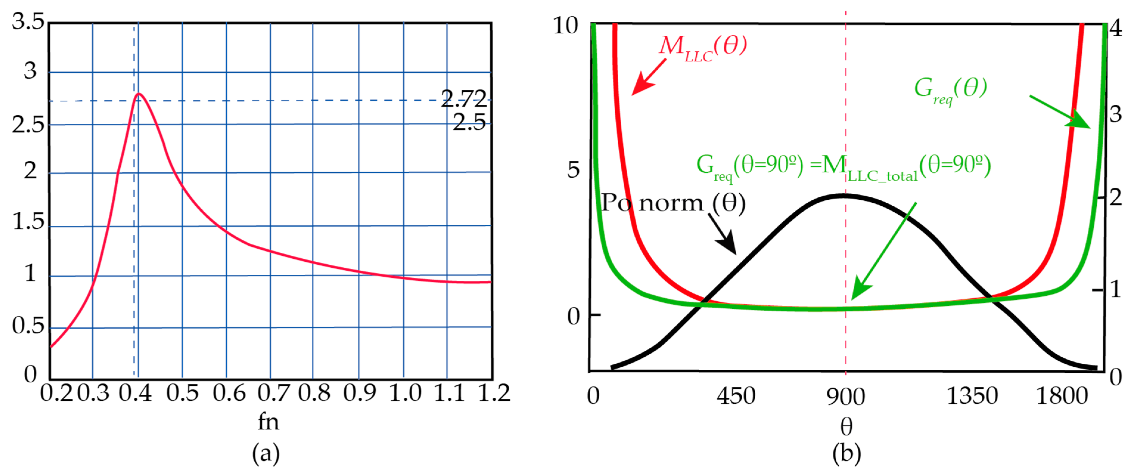
At the parallel resonance frequency
= 0.392, the proposed LLC resonant tank has a normalized gain of 2.71, which is 9% greater than the required gain of 2.5. If the LLC resonant converter gain will satisfy the PFC need at peak voltage, then it will fulfil the needs for the whole line voltage cycle. To assure zero voltage switching, the proposed GaN LLC converter is worked in an inductive region.
Figure 5 shows the proposed resonant converter’s typical voltage gain curve.
Table 1 contains all the basic design specifications of LLC resonant converters.
4. Design Consideration
In this section, we present a detailed design of the transistor, transformer, capacitor, and inductor for half-bridge LLC resonant converter.
Primary Transistors Selection: The following are key parameters for the selection of transistor for LLC resonant converter.
Dead time (
): The minimum dead time
of half-bridge LLC resonant converter for ZVS achievement can be calculated as:
Here, is time-related effective output capacitance.
Time related effective output capacitance (): For high-density and high-efficiency LLC converters, the transistor parameter defines the output capacitance required to transmit the voltage from the drain to the source passively. A shorter dead time and larger magnetizing inductance value for the transformer are made possible by a lower effective , which also reduces circulating losses on the primary side for provided drain-to-source transition time. Meanwhile, for a given value of and , the smaller value of , the larger can be utilized with ZVS condition to design a higher density LLC resonant converter.
This
derived from ‘Coss’ and
, which are related by the following equations:
Figure 6 presents the plots between
and
with
transition from 240 V to 0 V, Si MOSFET has 10 times larger
than GaN HEMT and SiC MOSFET has a 50
larger
than GaN HEMT.
and turn-off time (
:
, which defines the charge necessary for the gate to drain switching while the switching turn-off time
is another crucial transistor parameter for LLC resonant converter design. These two metrics indicate the efficiency and maximum operating frequency by indicating turn-off capabilities and losses. With the provided switching voltage and current circumstances, the turn-off time (
, which is often not listed in the transistor datasheet, can be approximated following the reference book [
32].
Reverse recovery charge (): The body diode’s current reverse recovery charge will produce high dv/dt and a significant shoot-through current that might cause a MOSFET breakdown in the bridging transistors. The lower the value, it is better to avoid failure since it is a crucial parameter for determining the hazard for the hard commutation failure mode.
Transformer: The detailed design of a high-frequency transformer is presented in this section. For the achievement of maximum efficiency and compatibility with the designed circuit parameters, the transformer design is carried out. For the core of the transformer, we use power ferrite 3C95 material from Ferroxcube to lower core loss. GaN HEMTs allow the LLC Resonant Converters to operate at a high switching frequency (Fsw), as described above. The effective core area (Ae) and primary side winding turns (N) decrease as the switching frequency rises. With the reduction in core size, the power density increases. The correlation between switching frequency and core size is shown in the form of magnetic flux density (B) Equation (20).
Equation (21) gives the transformer leakage inductance:
where N is the number of turns, bw is the breadth of winding, lw is the mean turn length, ‘M’ is the number of primary–secondary intersections,
h is the height of the primary-secondary intersection and hp is the height of pth winding portion.
By using the resistance factor
transformer ac resistance winding can be calculated as
where
is the penetration depth, m is the number of winding layers,
, h is the height of the conductor and
and
are the ac and dc winding resistance respectively.
Transformer inter-winding capacitance ‘C’ can be determined as
where ‘A’ is the area of winding,
is relative permittivity,
is the permittivity of free space, and ‘d’ is the distance between windings.
Inductor: In order to lower the inductor’s ac losses, two distinct windings (dc and ac windings) are used. Since thin ac windings have lower ac resistance, therefore they carry the majority of the ac ripple current. Similarly, thick dc windings have lower dc resistance; therefore, they carry the majority of the ad current. This will lower the inductor’s winding losses. As a result, efficiency will improve. We used Magnetics Kool Mμ core to minimize the core loss.
Equation (24) gives the value of the resonant inductor (
Equation (25) gives the value of magnetizing inductor (
)
The number of turns of the coupled inductor can be determined by Equation (26).
Capacitors: Ceramic capacitors are chosen for the input and output sides of the LLC resonant converter to decrease the size of the Equivalent Series Resistance (ESR) and converter. The value of the resonant capacitor is determined as:
Comparative Analysis of GaN HEMT and Si MOSFET for LLC Resonant Converter
The most modern Si-based MOSFET with an inherent fast body diode was selected for comparative analysis. The most recent wide bandgap HEMTs are more suitable for high-density and high-efficiency power conversions.
Table 2 demonstrates the advantages of GaN power transistors over Si for LLC resonant converter critical parameters. For the better performance of highly efficient and high power density LLC resonant converter designed, the values of
,
,
and
should be low. The GaN HEMT has lower values for all these parameters as compared to Si MOSFET. A lateral two-dimensional electron gas channel generated on a GaN heterojunction with no inherent bipolar body diode is another important feature of GaN power transistors for the design of high-efficiency LLC resonant converter. Without body diode for GaN HEMT,
is zero, which prevents the hard avalanche behavior as described above due to the presence of body diode for Si MOSFET. GaN FETs are the majority carriers, unlike Si MOSFETs. Therefore, there is no reverse recovery charge, hence no reverse recovery losses. Three types of losses occur in power switches that are: (1) conduction losses (determined by RDS(ON)) (2) driving losses (determined by Qg), and (3) switching-off losses (determined by Coss). We analyzed that the GS66508B has mentioned advantages for these losses reduction over the Si MOSFET IPx65R110CFD when working at higher frequency with soft-switching for half-bridge LLC resonant converter.
5. Simulation Results
The designed LLC resonant driver has output voltages of 60 V, 240 W output power and is driven by a 240 V AC at 75 kHz frequency. A thorough simulation analysis of the design converter is carried out to improve the design. The LLC resonant converter model is simulated on CADENCE under different test conditions to verify performance and operation.
Figure 7 shows the typical operational waveforms of the LLC resonant converter.
In
Table 3, all the losses of different components of LLC resonant converter are mentioned.
The computed percentage loss distribution of the converter at full load is shown in
Figure 8. Magnetic losses are responsible for about 40
of losses due to copper and core losses. Approximately 50
of the total losses are due to switch deriving and conduction losses.
It is clear from
Figure 9 GaN HEMT has a great advantage in both switching performance and conduction for LLC resonant converter applications.
Transformer primary terminal voltage and current, and rectifier output voltage is shown in
Figure 10. The waveform of rectifier output voltage is perfect square wave.
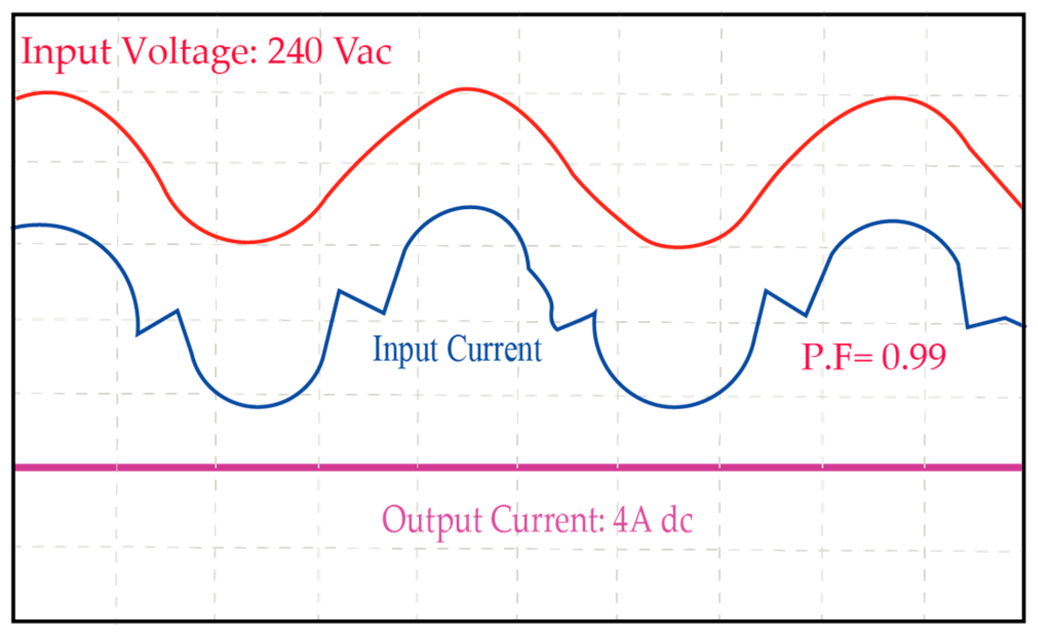
Figure 11 shows the input current, voltage and output current. A 0.99 power factor is achieved.
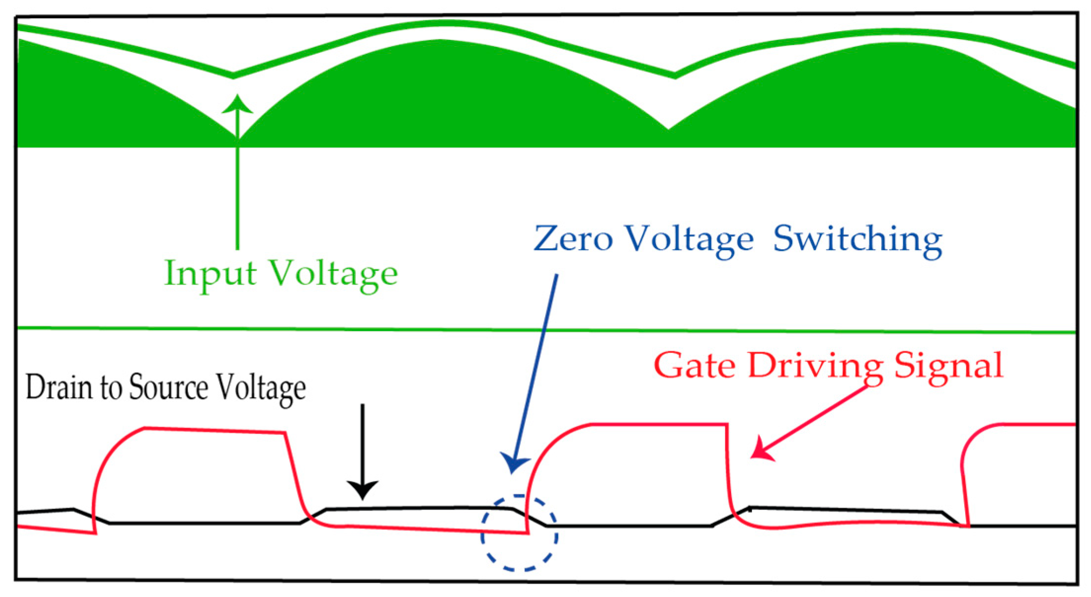
Figure 12 shows that ZVS performance was achieved during the whole LLC resonant converter operation. This significantly lowers switching loss and increases the overall efficiency of the converter.
The major loss differences come from the primary side transistors if the loss breakdown of other components, such as the inductor, capacitor and transformer, is expected to be the same. Even if the LLC converter achieves ZVS for turn-on, the switching turn-off loss persists with the magnetizing current on the main, especially at higher switching frequencies. Despite the fact that these turn-off losses cannot be ignored, GaN HEMTs have very low switching turn-off losses. In addition, the GaN-based LLC has very small drive losses. In short, the GaN-based LLC converter achieves excellent efficiency, and this increase in efficiency offers the incremental performance necessary for low-power applications to surpass the most recent industrial system requirements.
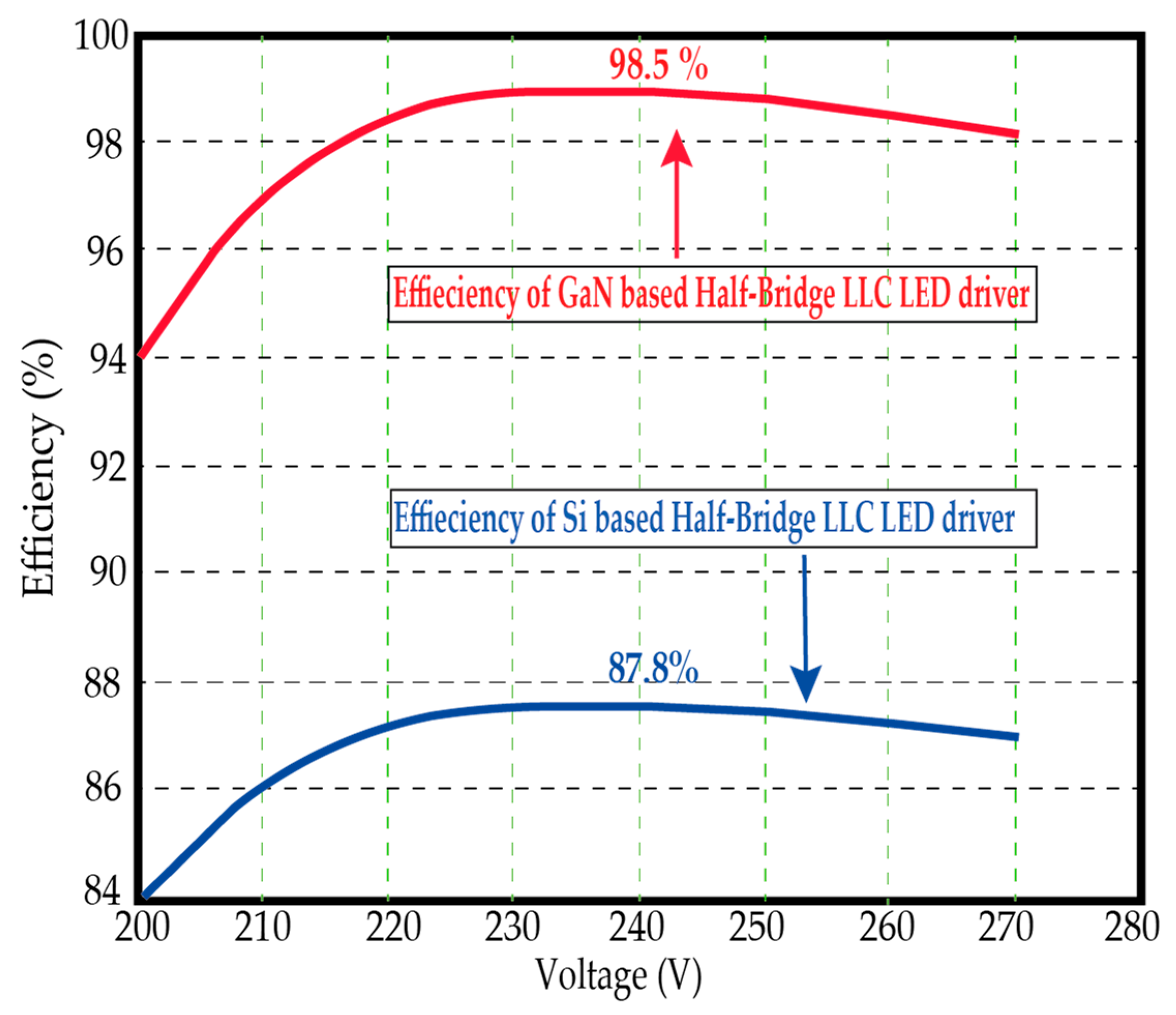
Figure 13 shows maximum efficiency at rated voltage and current, i.e., 240 V and 4 A. Such a highly efficient proposed design gives a cost-effective solution compared to a Si MOSFET-based LLC resonant converter. The maximum efficiency achieved for the proposed LLC resonant converter is 98.5%.
Figure 14 shows the power factor comparison of the two solutions. It is clear from the figure that the GaN HEMT solution has a much better power factor than the Si MOSFET solution.
Switching turn-off losses, which Si MOSFET has six times more than that of GaN HEMT, are the most significant losses for Si MOSFET-based LLC resonant converter compared to that of GaN HEMT. Additionally, the drive loss of the GaN LLC resonant converter is substantially lower than that of Si MOSFETs. Overall simulation results indicate that compared to Si, the GaN LLC resonant converter has around 37% fewer total losses.
Figure 15 shows the efficiency comparison of the two solutions. In summary, GaN LLC resonant converter achieves excellent efficiency. This increase in efficiency gives the incremental performance necessary for low-power applications to surpass the most recent industrial system requirements.
Compared to GaN HEMT-based LLC resonant converter, the switching turn-off losses for Si MOSFET-based LLC resonant converter are the most significant losses. In addition, GaN HEMTs-based resonant converter has a much lower drive than that of Si MOSFETs.
Overall simulation results indicate that compared to Si MOSFETs solution, the GaN LLC resonant converter has around 37% fewer total losses. A loss comparison of two solutions for LLC Resonant Converter is shown in
Figure 16, which shows that GaN HEMT has significant advantages on switching performance and conduction for LLC resonant converter design.
Table 4 shows that the LLC resonant converter design with GaN HEMT has great advantages over the Si MOSFET design.


