1. Introduction
Low-power wearable and implantable devices for long-term continuous monitoring of biopotential signals have been an important research topic with the prospect that they can improve people’s everyday life [
1]. In recent years, these monitoring devices have seen significant advancements, bringing the concept of a wireless body area network (WBAN) [
2]. WBANs are composed of several sensors connected through a network being able to detect and record biopotential signals to detect diseases and monitor the patient’s health.
Table 1 presents the amplitude and frequency range characteristics of some common biopotential signals that can be recorded to detect diseases and monitor the patient’s health [
3]. Low-power analog front-ends (AFEs) are used in the acquisition of such biopotential signals, which must comply with some sets of complex challenges, such as detecting the feeble biopotential signal while introducing minimum noise to the already weak signal for proper recording [
4] and providing high linearity [
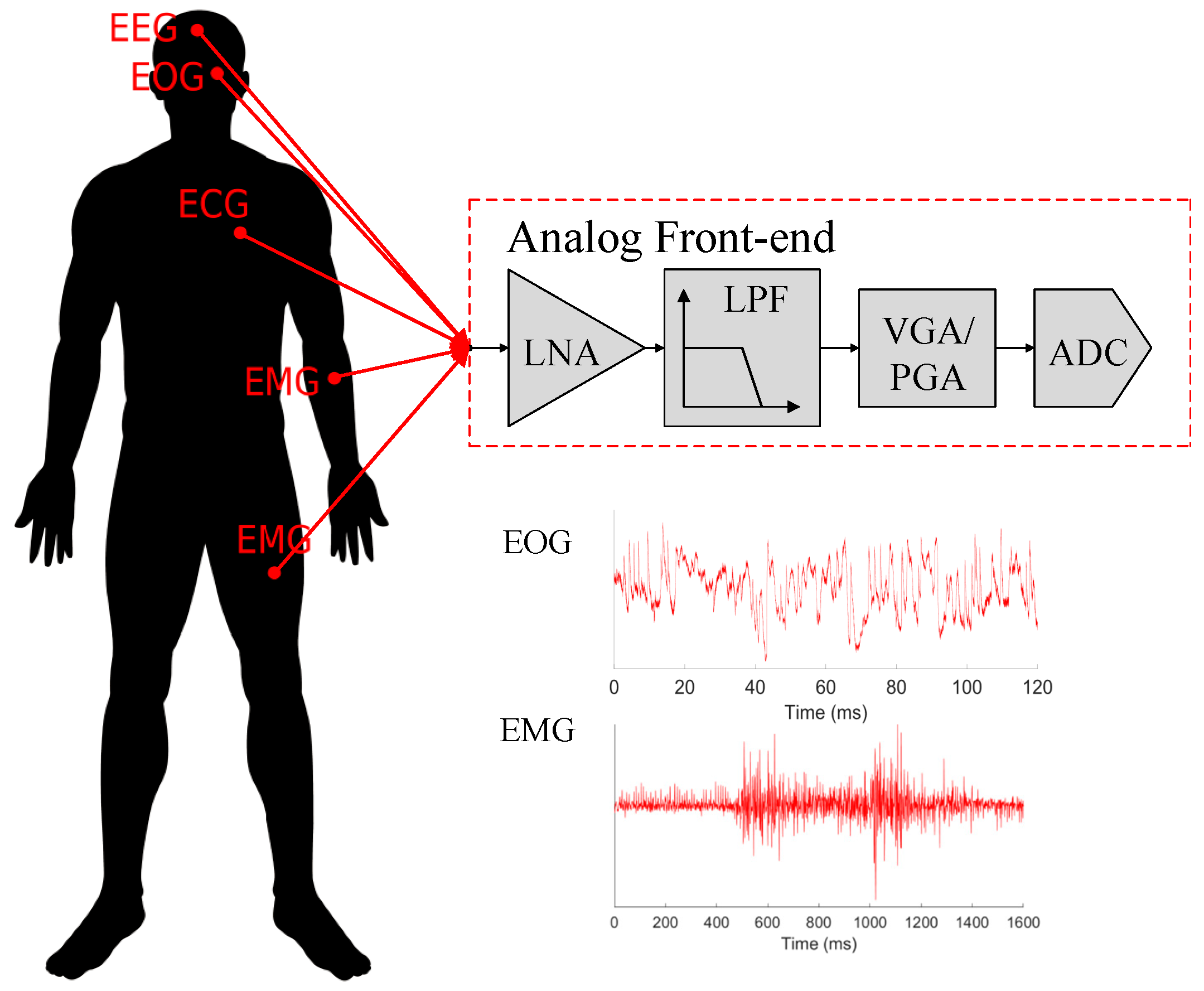
5]. Moreover, portable AFEs have even more restrictions since they have very limited current budgets and, therefore, they have low power consumption to extend the operation lifetime while presenting small form factors to be ergonomic and, hence, fully benefiting from dedicated integrated circuit solutions. The AFEs usually consist of four blocks: a low-noise amplifier (LNA), a filtering block, a variable-gain amplifier, and an analog-to-digital converter, as shown in
Figure 1, with the LNA being typically one of the most power-hungry blocks to reduce the noise introduced in the system. Yet, there are some AFEs that are used only for signal detection, normally presenting lower power consumptions with less constraint on the noise requirements [
6,
7].
This paper presents a low-power LNA for fully recording electromyogram (EMG) and electrooculogram (EOG) biopotential signals. This low-power LNA focuses on enabling two working modes with gain and cutoff frequencies that can be tuned for each biopotential signal. Moreover, the circuit has enough reconfigurability to achieve other gains and a wider range of cutoff frequencies.
The EMG signal has a maximum frequency range of 2000 Hz; the cutoff frequency respective to this mode should be around this value. This mode will be, from now on, mentioned as high cutoff frequency (HCF) mode. Analogously, the mode concerning the EOG signal is designated the low cutoff frequency (LCF). The LCF presents a higher gain since the input signal amplitude is lower, and its cutoff frequency should be over 10 Hz.
The main contributions of this study are: (1) The LNA presents an embedded tunable bandwidth (BW) with the use of a varactors’ system controlled by external voltages that enables BW to range from 13.5 Hz to 3 kHz. It also presents embedded pseudo-resistors that enable the gain’s tuning and is also controlled by an external voltage. This method can provide a gain range from 31 dB to 50 dB; (2) the LNA was conceptualized to accommodate the EMG and EOG biopotential signals, presenting two working modes, one with lower gain and higher BW for the EMG signal, and one higher gain and lower BW for the EOG; (3) the LNA was designed for noise minimization, consuming only 1.2 μW (including a self-biased current reference) while achieving competitive noise efficiency factor (NEF) and power efficiency factor (PEF) values; and (4) the circuit was fabricated and experimentally tested, showing the following specifications for the HCF mode: a gain of around 34.7 dB, a bandwidth (BW) of 1412 Hz, and an input referred noise of 1.407 μV, resulting in a NEF of 1.44 and PEF of 2.5, well on par with current state-of-the-art. The LCF’s experimental measures show: a 39.5 dB gain with a 22.4 Hz BW, input referred noise of 0.829 μV, and matching the NEF and PEF of 6.37 and 48.75, respectively. Both modes consume a current of 1 μA and present a total harmonic distortion (THD) under 1%.
The rest of this paper is organized as follows.
Section 2 discusses related work.
Section 3 explains the proposed LNA topology. In
Section 4, simulation results are shown, presenting the circuits tuning capability; the experimental results are shown in
Section 5; and finally, in
Section 6, conclusions are drawn.
2. Related Work
State-of-the-art LNAs for biopotential signal acquisition are typically composed of operational transconductance amplifiers (OTAs) presenting a fully differential capacitive feedback structure [
5,
6,
8,
9,
10,
11,
12,
13,
14,
15]. This structure provides the LNA with a band-pass response where its mid-band gain can be easily set by the ratio between the input and feedback capacitors. Due to the input capacitors, this feedback structure is a noiseless form of attenuating the dc offset from the electrodes. Moreover, by opting for a fully differential topology, it helps to achieve a high common-mode rejection ratio (CMRR) and power supply rejection ratio (PSRR) [
8]. Some work further introduces the feedback loop pseudo-resistors for better control in settling the LNA’s BW [
5,
6,
8,
9,
10,
13,
14,
16] or even provides BW tunability [
8]. Another development carried out on the capacitive feedback loop was the introduction of reset switches to initialize or reset the input and output standard mode voltages before the amplifier starts or when it is saturated [
16,
17]. An improvement over the conventional capacitive feedback is the T-network capacitive structure [
4,
18]. It has the advantage of reducing the sensitivity to mismatch and process variations by using larger capacitors with a small equivalent capacitance so that the input capacitor may be smaller.
LNAs are usually divided into two groups, the ones for signal detection and the ones for signal recording. The first group is characterized by presenting very low power consumption but higher noise values [
6,
8,
9]. These LNAs are usually formed by simpler OTA topologies with a capacitive feedback structure to reduce the voltage supply and present a band-pass response. On the contrary, the latter target the acquisition of the signal in a truthful data stream, leading to LNAs showing higher power consumption and lower noise values [
10,
11,
12,
19]. These LNAs have more complex OTA topologies using techniques such as inverter-based input stages to reduce the noise and increase the transconductance under a given current, biasing the transistor in the sub-threshold region, use chopper modulation, and even stacking OTAs or input stages for current reuse to reduce their power consumption while maintaining a low noise level [
4,
10,
11,
13,
14]. In Reference [
10], a driving circuit is embedded in the inverter-based input stage to stabilize the current at the output stage, thus maximizing the current efficiency. Others, such as [
13] or [
14], use this technique for multi-channel applications. The first presents two folded-cascode amplifiers sharing a mid-rail current sink/source and current source, whereas the second explores a binary tree structure with several input differential pairs across multiple stages. This amplifier requires an output recombination stage that generates the output voltage by summing the output currents. Reference [
11] also uses the current reuse technique on a folded-cascode amplifier. However, its focus is controlling the noise level on different channels by providing more power to the ones where the signal is detected.
To further reduce the noise levels, other LNAs use chopper modulation techniques [
9,
11,
12,
13,
15,
20]. By implementing choppers, the 1/f noise and dc offset are attenuated. However, its implementation has drawbacks since the choppers produce ripple and present limited input impedance, which must be mitigated with additional circuitry. The most common way to increase the input impedance is by using an impedance boosting loop [
9] or a positive feedback loop [
12,
18]. An innovative form was developed in [
20], which uses an input sampling input stage and digital–analog hybrid dc servo loop. As for chopping ripple suppression, it usually used a ripple reduction loop [
12,
20]; alternatively, a strategy can be the implementation of an auto-zero offset cancelation loop [
18].
From these works, it can be seen that the LNAs can be more flexible since different biopotential signals have different characteristics in terms of voltage and bandwidth. By using tunable pseudo-resistors and tunable varactors the proposed LNA can present specifications of each intended biopotential signal. Moreover, the tunability is implemented while maintaining a very competitive noise result and power efficiency.
Before moving on, it is also important to introduce two important performance figures for LNAs. A key figure when comparing LNAs is the NEF. It was first introduced in [
21] and relates the input noise levels to the current consumption. It is expressed as:
where
Itot is the total current consumed,
UT is the thermal voltage,
k is the Boltzmann constant,
T is the temperature, and
BW is the bandwidth. Later, in [
22], the authors introduced the PEF, which is formulated as:
for improved comparison between LNAs with multiple power supplies.
3. Topology Description
The topology presented in this paper is based on the fully differential inverter-based current-mode IA from [
19], with additional embedded tunable gain and tunable BW, as shown in
Figure 2. It was first presented in [
23], however, only at the post-layout level and developed in a 130 nm node. In this topology the tunable cutoff frequency is done with a varactor system that includes a bank of varactors for each cutoff frequency, being turned on and off according to the desired mode. The cutoff frequencies are set with an external control voltage (
VCTRL) and two external control voltages (
VH and
VL) that turn the modes on and off. The embedded tunable gain is implemented by replacing R2 with pseudo-resistors (P2) also controlled by the same external voltage (
VCTRL) that controls the cutoff frequency. This enables each mode to have its specific gain and cutoff frequency; however, in general, for a different application, the circuit may have different control voltages to tune the gain and BW independently.
The current-mode IA is a differential input–output amplifier with an inverter input stage (N1 and P1). The inverter, as the input stage, is used to reduce the noise level at this stage by doubling the transconductance under a given current. Plus, the gm/id is higher when biased in the sub-threshold region. Moreover, it is possible to reduce the input-referred noise (IRN) further if the inverter transistors at the input stage have a large area [
10] since it reduces the flicker noise, which is the main type of noise contributor in these types of applications. The transistor N2 acts as a common-mode feedback loop, as it sets the current at the input as well as the common mode at the output of this stage. In the second stage, there is a transimpedance amplifier (N3), which sets the output gain with the resistor R1 and the pseudo-resistors P2. The amplifier’s gain is attained from the LNA’s small-signal equivalent circuit presented in
Figure 3 and follows the following expression:
where α
1 is defined by:
Although in [
19], it is mentioned that the gain, with some approximations and considerations, can be expressed as:
In this case, these mentioned approximations are not possible due to the much smaller current budget, although one may conclude that the ratio P2/R1 is proportional to the gain, meaning that if the ratio increases, the gain also increases. Other considerations about these two components are that the resistor R1 is directly linked to the noise performance, whereas the pseudo-resistors P2 are linked to the linearity. Both the noise and linearity increase with the increase in the respective component. Thus, adjusting the gain by tuning the P2/R1 ratio is easy. However, a trade-off between linearity and noise has to be considered. The circuit has more pseudo-resistors, the N4 devices that sense the common mode at the output stage. Therefore, along with N5, they operate as a common-mode feedback loop and define the current at this stage.
A varactor system for the cutoff frequency tuning is implemented between the first and second stages. The tunable varactor system is implemented with two pairs of varactors, one for each mode. The one respective to HCF was designed for a cutoff frequency for the EMG signal around 2000 Hz, and the one respective to LCF for a cutoff frequency over 20 Hz for the EOG signal. The varactors are a transistor with a structure that creates a capacitance effect with a small drawback in terms of area or noise introduction. In this work, the varactors have a D=S=B structure, meaning the drain, source, and bulk are connected. This connection establishes a capacitance with the gate (
VBG), with the capacitance being tuned according to the voltage at the D=S=B port. It was chosen since it is the only structure that works in multiple regions [
24]. The total varactor capacitance can be given by
, where C is the capacitance per unit of area and S is the transistors channel area [
25]. The maximum capacitance per unit can only be achieved in strong inversion (if the bulk-gate voltage is much higher than the threshold voltage,
VBG >>
VT) or accumulation (if the bulk voltage is lower than the gate voltage,
VB <
VG) regions [
26]. After each varactor, there is another transistor working as a switch to turn it on or off. This switch is controlled by external control voltages
VH (for the HCF varactors) and
VL (for the LCF varactors).
The pseudo-resistors (P2) are implemented using PMOS with a configuration consisting of the bulk connected to its drain, as shown in
Figure 4. Due to the dependency of the threshold voltage on the substrate potential, this method results in a finite large equivalent resistance instead of an almost infinite impedance [
27]. The pseudo-resistors can work in the cutoff region, presenting high resistance values in the giga-ohm order or, in the triode region, with lower resistances values of kilo-ohms [
28], with the tuning being done by the external control voltage. The tuning feature enables different gains for each signal since they also present different amplitudes. When
VCTRL = 1.2 V, the gain is higher than when
VCTRL is 0 V. The control code is
VCTRL = 0 V,
VH = 0 V, and
VL = 1.2 V for the HCF mode, and
VCTRL = 1.2 V,
VH = 1.2 V, and
VL = 0 V for the LCF mode.
The fabricated circuit also includes a self-biased Widlar current reference for the LNA biasing, as in
Figure 2. The current reference consumes 0.25 μA from the 1 μA current budget used in total.
4. Simulation Results
The fabricated sizing is shown in
Table 2. The full layout is shown in
Figure 5 and occupies an area of 0.624 mm
2 (964.66 μm × 647.47 μm), with pads included. A major part of its area is occupied by a large bank of varactors that establish a low cutoff frequency of around 20 Hz.
The simulation results from the post-layout analysis are summarized in
Table 3.
Figure 6 and
Figure 7 show the post-layout simulated results, where a gain of 34.8 dB with a BW of 2.06 kHz is expected for the HCF mode; as for the LCF mode, the simulated gain is 40 dB, and the BW is 20.5 Hz. The IRN for the HCF is 1.61 μV matching a NEF of 1.37 and a PEF of 2.24, whereas, for the LCF mode, the IRN is 0.407 μV, with a NEF of 3.46, and 14.36, respectively.
The LNA shows good linearity in comparison to state-of-the-art works with a THD under 1% for both modes. The CMRR and PSRR simulated values were obtained from a 500-run Monte-Carlo σ = 3 simulation, considering process and mismatch variations, and the results were obtained from the minimum value in the respective BW; therefore, the HCF presents a CMRR mean value of 88.9 dB with a standard deviation of 6.7 and the LCF a mean value of 78.8 dB with a standard deviation 8.3, as seen in
Figure 8. In
Figure 9, the PSRR histograms are illustrated for both the HCF and LCF obtained the same way as the CMRR previously, and the HCF case has a mean value of 98 dB with a 5 dB standard deviation, whereas the LCF presents a PSRR mean value of 90 dB and 5.2 standard deviation.
To consider the circuit’s variability in process and mismatch in regard to the other metrics, a 500-run Monte-Carlo σ = 3 simulation was performed. From the results shown in
Figure 10,
Figure 11 and
Figure 12 concerning the HCF mode the gain, BW, and IRN present mean values of 34.7 dB, 2.1 kHz, and 1.6 μV with standard deviations of 0.8 dB, 313.5 Hz, and 78 nV, respectively. Regarding the LCF, mode gain has a mean value of 40 dB with a standard deviation of 1.3 dB, the BW shows a mean value of 20.9 Hz with a standard deviation of 3.6 Hz and the IRN presents a mean value of 330.3 nV with a standard deviation of 12.1 nV. From these results, one may conclude that the circuit has low variability, especially in terms of the input noise. It is also important to note that while gain and bandwidth have a larger variation they can be tuned after fabrication.
Although when manufactured the LNA had the same
VCTRL connected to the pseudo-resistors (P2) and the varactors to tune the gain and BW, respectively, for other applications, it may be separated, thus having a control voltage to tune the gain and a different one to tune the BW. To check the potential gain and BW ranges, the LNA was simulated with one control voltage to set the gain and another one to set the BW. First, the gain range in both modes, the varactors’ control voltage is set to 0 V so that it has the same BW as in the HCF mode, and to 1.2 V to set the LCF’s BW. The results obtained are shown in
Figure 13 and
Figure 14, respectively. From
Figure 13 one may perceive that as expected the gain increases until
VCTRL reaches around 0.4 V and stabilizes from then on, presenting a tuning range from 34.7 to 51.1 dB.
Figure 14 shows that the gain decreases with the decrease in
VCTRL achieving a value of 30.8 dB.
The BW’s tuning range is analyzed in
Figure 15 and
Figure 16; for these simulations, P2′s voltage control is set with 0 V and 1.2 V, respectively, as in the HCF and LCF modes. In
Figure 15 the BW ranges from 0.851 kHz to 3 kHz, whereas in
Figure 16 the BW ranges from 13.5 Hz to 24 Hz when the gain at 1 Hz is similar (0.1 dB variation), from
VCTRL = 0.9 V to
VCTRL = 1.2 V the BW’s control voltage begins to influence the low-frequency gain.
For a better understanding of the circuit, it is also interesting to see the resistance values that pseudo-resistors P2 can achieve with the variation of
VCTRL. This simulation was made by applying a square wave at the circuit’s input and obtaining the output voltage and the current between the pseudo-resistors when the signal was high and low. In both cases, the pseudo-resistor had very identical values. In
Figure 17 is perceived that the pseudo-resistors have a very high resistance variation, particularly from 0.4 V to 0.9 V. The resistance value of P2 varies from 4.36 MΩ to 2.38 TΩ.
5. Experimental Results
The proposed low-power LNA was fabricated in 110 nm UMC technology and wire-bonded to the printed circuit board (PCB) shown in
Figure 18a; in
Figure 18b a photograph of the die is shown. For measurement, and since the LNA presents differential input and output, its outputs were applied to a pre-amplifier (SRS SIM910 JFET Preamp) with unitary gain set for most measures, to convert it from differential to single-ended.
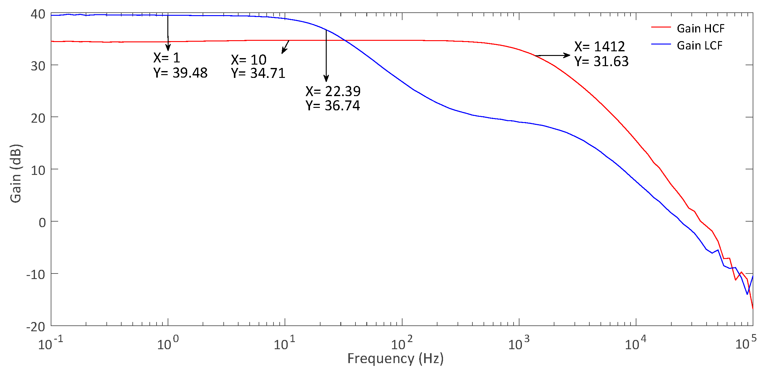
The measured current consumption is 1 μA without the PCB’s extra circuitry. The measured LNA’s dc output was 492 mV with a deviation under 3 mV while presenting an input impedance of 7.48 MΩ. The LNA’s ac responses for both modes were measured using Analog Discovery 2 and are shown in
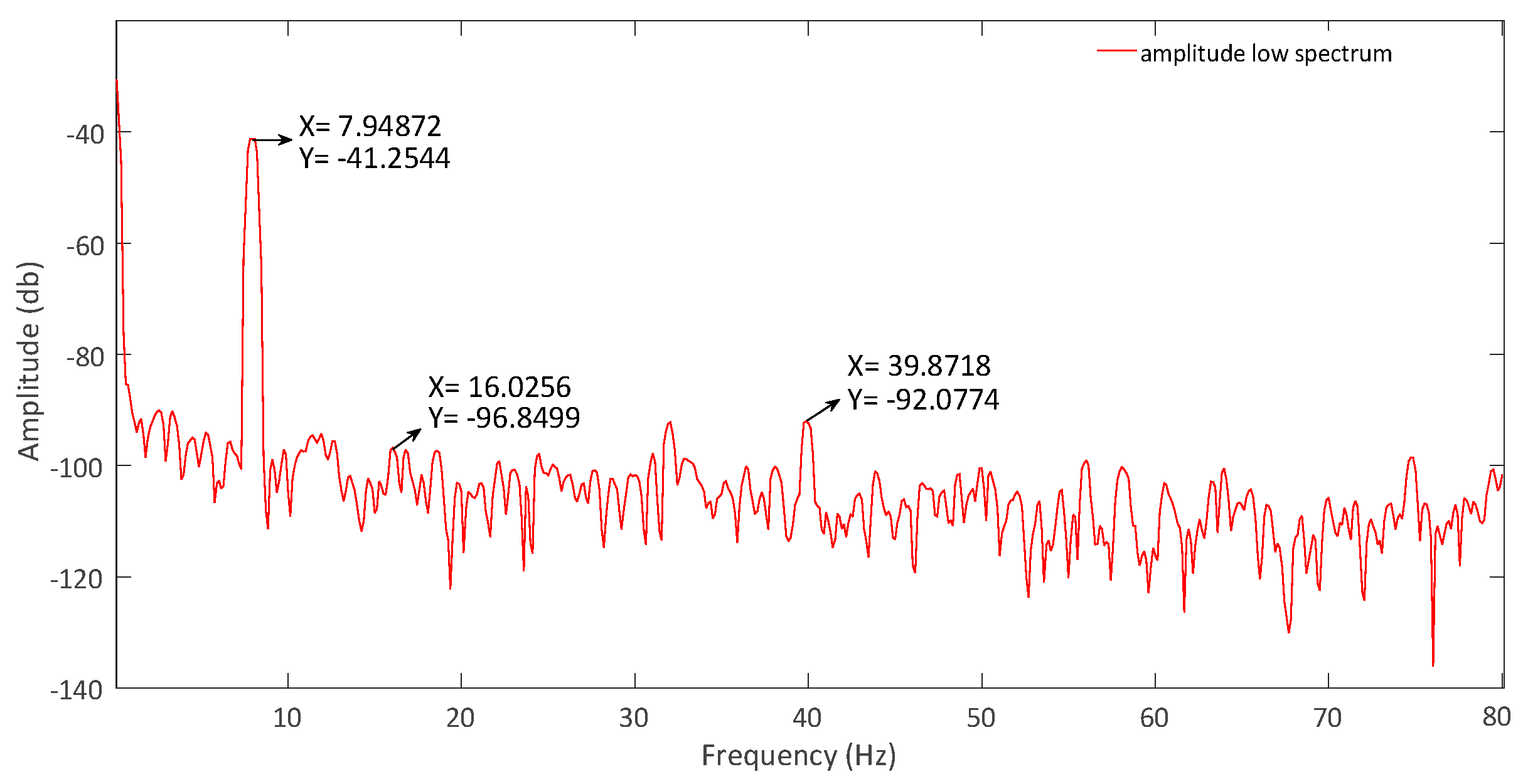
Figure 19. It depicts an HCF gain of 34.7 dB and a BW of 1412 Hz, an LCF gain of 39.5 dB, and a BW of 22.4 Hz. To measure the signal’s linearity after amplification, a 1.85 mV and 120 Hz sinusoidal signal was set at the input of the amplifier in HCF mode. The resultant fast Fourier transform (FFT) is in
Figure 20, where a THD of 0.68% is obtained. In the LCF mode, the input signal was 630 μV with a frequency of 8 Hz. The THD achieved was 0.46%, and its FFT is in
Figure 21.
The measured input noise voltage spectral density of both modes is shown in
Figure 22 and
Figure 23. The noise measurements were done with the common mode applied to the LNA. For this measurement, the preamplifier’s gain was set to 50 to amplify the LNA’s noise above the noise floor of the baseband signal analyzer. The noise measurement had to be done from 1 Hz since the minimum BW resolution of the baseband signal analyzer is 0.5 Hz. In addition to the measured noise from the LNA, the noise from the preamplifier and baseband signal analyzer was also measured to remove their interference from the measured noise. In
Figure 22 and
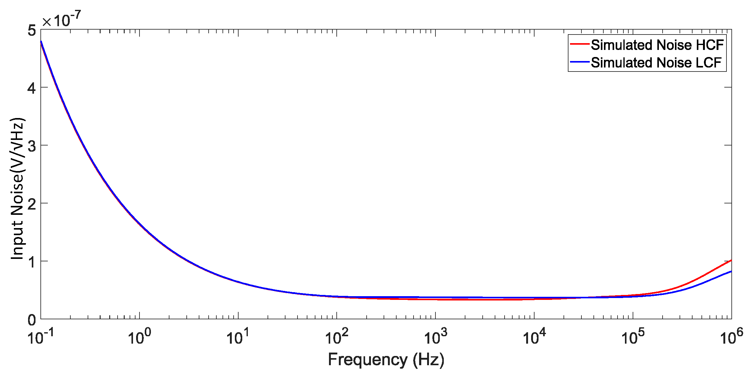
Figure 23, the 50 Hz line interference can be observed since it was not attenuated by any extra circuit, the influence is considerable, yet it was not removed for the noise calculations. Thus, integrating the input noise voltage spectral density from 1 Hz to each mode BW, 1412 Hz (HCF) and 22.4 Hz (LCF), an IRN of 1.407 μV, a NEF of 1.44 and a PEF of 2.5 is calculated for the HCF mode. In the LCF mode, the IRN is 0.829 μV, corresponding to a NEF and PEF of 6.37 and 48.75, respectively.
The CMRR and PSRR measures were also obtained using Analog Discovery 2. The PSRR and CMRR results are shown in
Figure 24 and
Figure 25, depicting values of minimum values in their BW of 79 dB and 56.7 dB for HCF, whereas for LCF, the measures show values of 75.7 dB and 58.9 dB, respectively. These values are without considering the 50 Hz interference, which has a significant influence, especially in the PSRR measures. The discrepancies between the simulated and measured results are mainly seen under 4 Hz, especially in the LCF mode in terms of noise, which is likely to be introduced by the varactors. The BW is another metric that has a high variance between the simulated and experimental results, this occurs due to the input impedance of the preamplifier and Analog Discovery 2 which were not considered in post-layout simulations.
The summarized experimental results, along with other state-of-the-art LNAs in the recent bibliography, are presented in
Table 4. This work achieves the desired tunability with bandwidths of 20 Hz and 1.4 kHz for gains of 34 dB and 39.5 dB. While consuming only 1 µA, very competitive noise results are achieved, namely, HCF’s mode IRN, NEF, and PEF 1.407 μV, 1.44, and 2.5, respectively, with the NEF being the lowest measured among the state-of-the-art.
6. Conclusions
This paper presents a low-power LNA based on a current mode instrumentation amplifier, with tunable gain and tunable BW, controlled from an external source, with two main working modes for biopotential signals, the EMG and EOG. The reconfigurability features are provided using tunable pseudo-resistors for the gain, and a tunable varactor system for the BW, controlled with an external voltage. Although the circuit was fabricated using only one control voltage for the tuning of both the gain and the BW, if a control voltage is implemented for each, the circuit can achieve a maximum tuning gain of around 16 dB and a maximum BW tuning of 2.17 kHz on the HCF mode. The LNA was manufactured using the UMC 110 nm design kit, and experimental results show gains of 34.7 dB and 39.5 dB for the HCF and LCF modes, respectively. With its 1 μA consumption and IRN of 1.44 µV rms noise, it achieves very competitive noise performance.


 ,
, 


