1. Introduction
Gallium nitride (GaN)-based power transistors are good candidates for the next generation of high-efficiency and high switching frequency converters [
1,
2,
3,
4,
5]. Among the presently commercialized semiconductors, GaN has the widest energy gap, the largest critical field, and the highest saturation velocity [
6].
The most common GaN transistors today are high electron mobility transistors (HEMT) based on the 2D electron gas (2DEG) channel created by an heterojunction, usually AlGaN/GaN [
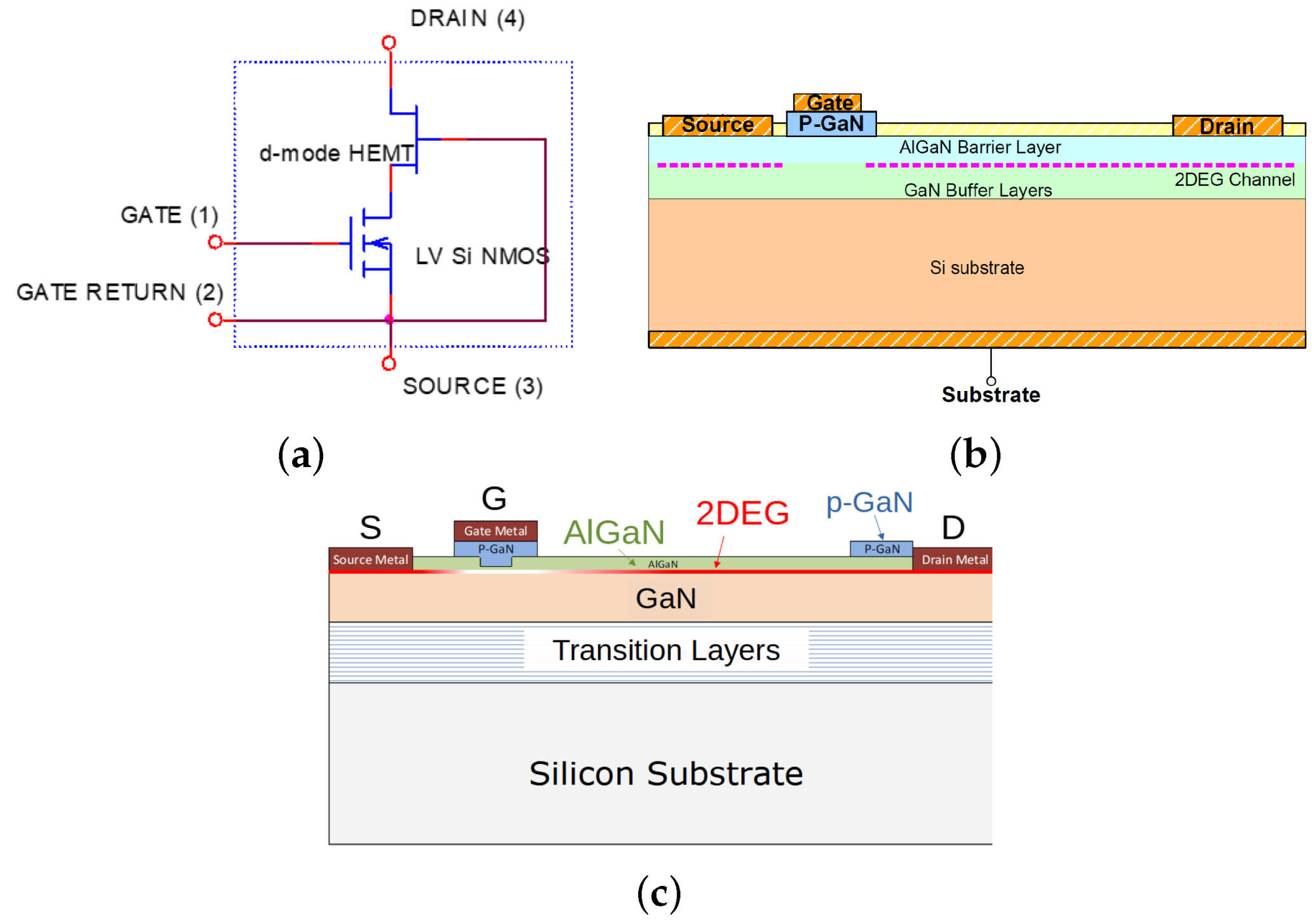
1]. Different technologies have been developed to produce normally-OFF HEMTs, and among the most commonly used and studied are the cascode structure [
1], the gate-injection transistor, or GIT (also refereed to as p-GaN gate HEMT) [
7], and the gate-injection transistor with hybrid drain (HD-GIT).
The p-GaN gate HEMTs present a threshold voltage (
) instability dependent on both the voltage bias stress level [
8,
9,
10,
11,
12] and temperature [
12,
13]. This variation of
is often associated with trapping mechanisms near the 2DEG channel in the region under and around the gate [
14,
15], but was also explained with the charging and discharging of the gate p-GaN layer, which has a semi-floating potential [
16].
The fluctuation of the threshold voltage can introduce serious reliability issues, particularly in systems where a higher switching frequency is desired [
1,
8]. Parallel to that, some of the degradation mechanisms in GaN HEMT are accompanied by a
shift [
9,
17], and having a well established protocol to characterize it could contribute to the research in these topics [
18].
The
instability phenomenon is also present in SiC MOSFETs [
19,
20,
21], although due to different charging mechanisms. In SiC MOSFETs, it occurs due to the charging and discharging of gate traps, depending on the traps at the interface between the gate oxide and the semiconductor; and the border traps in the gate oxide near the interface [
19,
22].
However, what both these mechanisms have in common is the circulation of electric charge in and out of the gate structure, distinct as these may be. Therefore, it is possible that the measurement protocols established to deal with the instabilities in SiC MOSFETs could also have stabilizing effects on the of p-GaN gate GaN HEMTs.
The goal of this study is to determine if the
measurement protocols established initially for SiC MOSFETs can be applied to GaN HEMTs. Particularly, the applicability of the triple sense
measurement protocol established by the JEDEC standard JEP184 [
23] will be used to study the characteristics of the
shift on HEMTs.
It is important to highlight the fact that, even though the protocol has been defined for and previously tested on SiC MOSFET, there is no occurrence in the literature of this protocol being applied to GaN transistors of any kind. Moreover, the triple sense protocol can be performed in two different orders, depending on the initial gate polarization, and an experimental study can determine which is the best definition of the protocol for GaN HEMTs.
This study is based on two GaN HEMT devices commercially available, from different manufacturers. They are of different technologies: the gate-injection transistor (GIT) and the gate-injection with hybrid drain (HD-GIT). Additionally, a cascode structure is introduced in the context section.
This paper is structured as follows:
Section 2 establishes the context of the study, resuming the characteristics of each device under study and discussing the
instability phenomenon.
Section 3 describes the measurement protocol proposed to increase the stability of
measurement, and
Section 4 details the results of the measurement series with and without a preconditioning protocol. The differences between these two approaches and the applicability of the proposed protocol are discussed in
Section 5.
3. Measurement Protocol
The standard JEDEC JEP184 proposes different protocols to characterize the
shift in SiC MOSFETs, and among these the triple sense protocol allows the most complete description of the phenomenon. It allows the identification of four components of the
instability, defined in the standard as follows [
23]: the drift
is a “permanent component” of the
shift, i.e., a variation from the initial measurement that remains constant on subsequent measurements; the transitory effects
, and the hysteresis
calculated as the difference between two
measured after two bias stress of different polarities, and any variation on the hysteresis
. In this paper,
is threshold voltage measured following a positive gate stress, and
for a negative gate stress. Therefore,
.
The triple sense protocol can be established with two different combinations, represented in
Figure 3a: either starting with a negative preconditioning bias stress (NBS protocol, or NBSP), or a positive preconditioning bias stress (PBS protocol, or PBSP).
The present work aims at determining which of these two combinations, NBSP or PBSP, is the most effective for GaN HEMTs.
There are four parameters on the triple sense protocol that must be adequately chosen and/or controlled: The preconditioning stress voltage level and time duration ; the sweep measurement time duration and the waiting time between the preconditioning stress and the sweep measurement .
The preconditioning voltage
can be chosen to correspond to the application gating voltages, but of course this is not mandatory. The stress should be applied for a time duration
long enough to stabilize the
shift. Such a configuration allows the emulation of the “steady-sate” behavior of the gate charges [
8].
However, a more thorough study would be necessary to determine values for and that can be applied to GaN GITs in general, or even to optimize the characterization protocol.
The
time should be as small as possible, because both the
and the
stress can affect the state of the charges in the gate [
8,
11]. The
is then calculated with an interpolation of the measured
.
The waiting time
should also be as small as possible, because a recovery time after the bias stress allows the gate charges to go back to their original states [
8,
10,
12]. More importantly,
has to be the same for each measurement, to ensure that the state of the gate charges are as similar as possible during the
measurement sweep.
For
to be short and adequately controlled with a Keysight B1505A, the waveforms shown in
Figure 3a were programmed in HP BASIC.
The voltage level of the preconditioning stress
was chosen by the authors to correspond to the on/off values recommended on the application notes of each device; they are summarized in
Table 4. This choice was made with the goal to mimic the conditions of a device under switching stress. The stress was applied for
ms for all devices, matching the order of magnitude of the protocol developed for SiC MOSFETs. As aforementioned, both
and
can be optimized in a future study.
The signal generated by the Keysight B1505A programmed in HP BASIC was measured with a scope and is plotted in
Figure 3b. The
ramp was programmed with a measurement step of
mV on
in order to keep
small, of the order of hundreds of milliseconds. This step was chosen to keep the measurement time small, to reduce the
stress over the DUS. If this stress is too long, it can compromise the stability of the characterization protocol.
Comparisons between direct and preconditioned sweep measurements are made for the same measurement step, so that the variation measured for each of these protocols is comparable.
The measurement programmed on HP BASIC allowed a reproducible
of the order of
ms. The
measurement is taken at the values of the drain current
specified in the datasheet of each component, i.e., the values given in the fourth column of
Table 1.
All the measurements described in the paper were performed at constant ambient temperature (25
C). The literature indicates that lower temperatures increase the recovery of the threshold voltage shift [
8]. As a result, conducting this study under ambient temperature constitutes a worst-case scenario.
4. Results and Discussion
The results presented in this section determine whether the triple sense protocol is also effective for GaN HEMTs, and which of the NBSP or PBSP protocols should be recommended for these devices.
The variation of the
measurement results with both the PBSP and NBPS protocols are compared in
Section 4.1, to establish if one guarantees more stable results then the other.
The robustness of the chosen protocol is tested after static stress on the devices; the results are described in
Section 4.2.
4.1. Stability: NBSP vs. PBSP
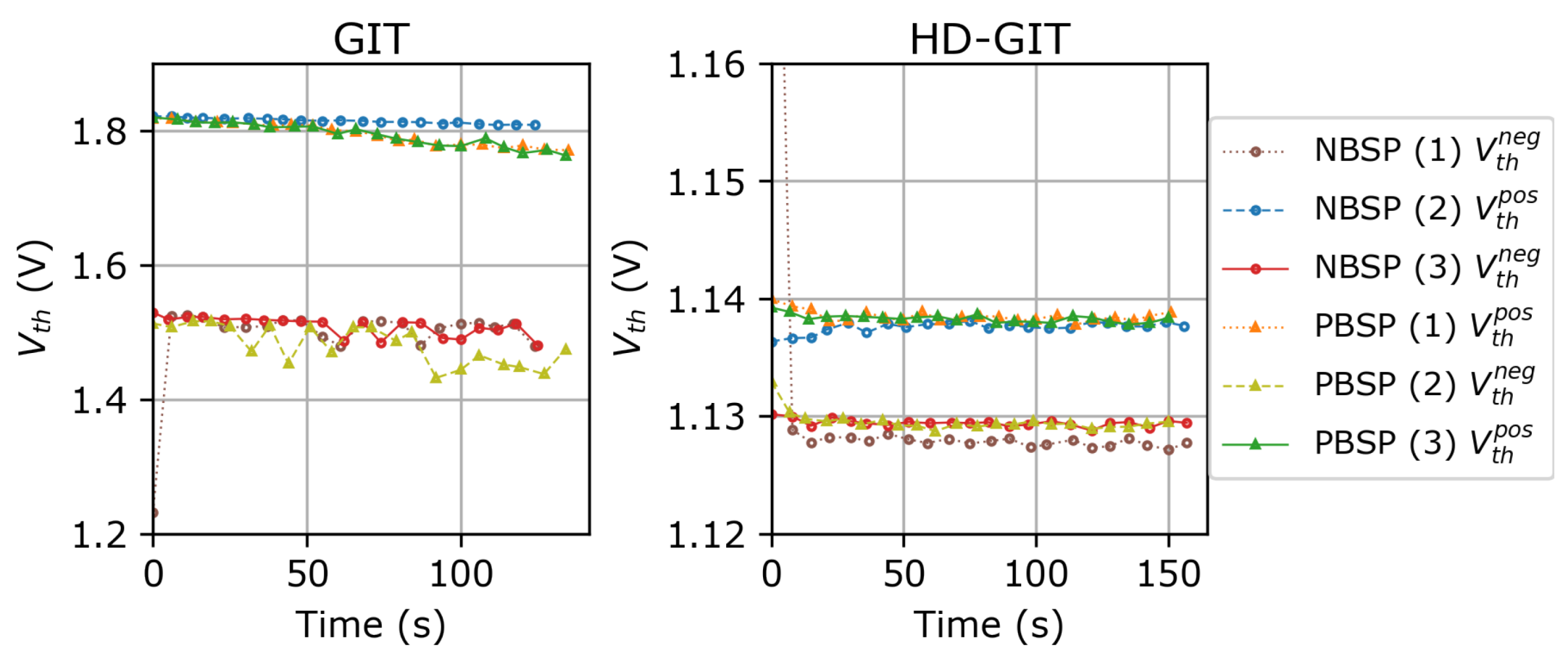
The stability of the results obtained with either the NBSP and PBSP protocols is compared through three separate series of 21 triple-sense preconditioned
measurements. The results for a single series are plotted for each device in
Figure 4.
Figure 4 shows that both of the devices present a visible hysteresis
, even if for the HD-GIT device it is relatively small. The results of the GIT have higher variation of the second
measurement with the PBS protocol.
To ascertain which protocol provided more stable results, the mean values and the
confidence interval (
) of each of the
measurements are resumed in
Table 5. Each entry in the table is calculated from a data set of size
and assuming a normal distribution.
For the GIT device, the NBSP configuration proved to give more stable results than the PBSP. For the HD-GIT, there was no difference in the stability for these two protocols.
An hysteresis of
V was measured in the GIT, while the hysteresis in the HD-GIT is too small when compared to the
mV step of the
sweep measurement, and therefore cannot be determined with sufficient accuracy. It is important to highlight that these hysteresis values could be higher if measured with fast measurements as in [
8,
16].
The HD-GIT device presented less hysteresis and instability because of the hybrid drain: the p-GaN layer on the drain promotes detrapping around the 2DEG channel, making the device less prone to both the current collapse and the instability.
Based on the results of this section, the authors recommend the NBS protocol as best adapted for GaN HEMTs, and will be using this version of the triple sense protocol in the rest of the paper.
4.2. Robustness: Reproducibility after Static Stress
To further test the reproducibility of the preconditioned measurements, experiments to ascertain the robustness of the protocol in devices under stress were performed. The NBS protocol was applied after each DUS was submitted to static voltage stress, from both and . The results are compared with those of a simple sweep measurement for each bias stress.
The chosen values for the bias stress are summarized in
Table 6. For both the GIT and the HD-GIT, the limit voltages were used. Each bias stress was applied for
s.
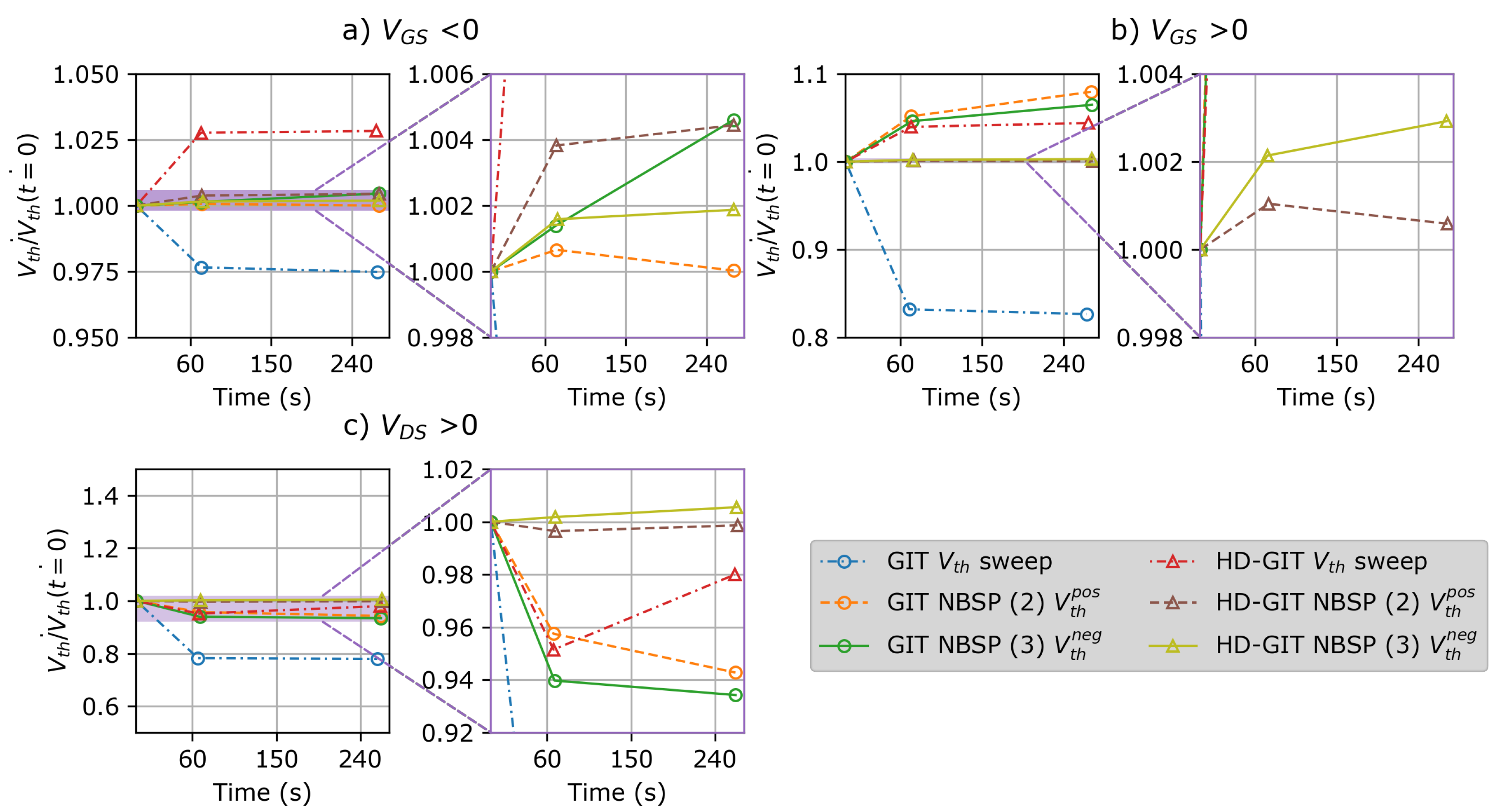
Three series of measurements were performed for each device and each static stress type. The results of a single series are presented in
Figure 5, normalized to the first
measurement (
) for each set. Therefore,
Figure 5 shows the variation of the measured value of
vs. time.
To analyze the robustness of the
protocol in more detail,
Table 7 summarizes the maximal variation of
for each device and type of static stress. The variations are calculated relative to
s), i.e., the measurement result on the recovered device.
For the two devices, the standalone sweep measurement presented a variation up to 10 times higher than that of the preconditioned measurement. Therefore, for these two technologies, the preconditioning measurement protocol gives more robust results even after the device was submitted to bias stress.
In conclusion, the preconditioning is indispensable to obtain repeatable measurements of the , because it emulates the charging state of the gate under stress in a switching application. Moreover, for the GIT technology the NBS protocol guarantees more stable measurement results even after the devices were submitted to stress.
5. Discussion and Applications
The triple sense protocol first established for SiC MOSFETs presented a good performance when applied to GaN HEMTs, particularly increasing both the stability and the robustness of the measurement results for the GIT-based technologies.
Having a stable and robust
measurement protocol established for GaN HEMTs will contribute to both the discussion on qualifying standards and the development of the research on the reliability and robustness of these devices. Indeed, the literature mentions degradation mechanisms in GaN HEMTs that are accompanied by a
shift [
9].
The triple sense protocol can help establish the medium- and long-term impact of typical stressing elements known to degrade GaN HEMTs, such as static drain-source stress in the OFF state, or hard switching [
25,
30,
31].
An example of an application of the triple sense preconditioning protocol is given in
Figure 6. The GIT device was submitted to a series of
V static stress lasting
s, and the
was measured using either the NBS protocol or the direct
sweep after each stress. The
values obtained with the direct sweep vary constantly, but the NBSP was able to stabilize it, again proving its robustness. It shows that the measurement of
with the triple sense protocol is a more reliable method to ascertain the effect of any degrading stress on the transistor.
The results in this study show that the preconditioning stress included in the protocol was able to stabilize the results of the measurements. Therefore, it is proven that the triple sense protocol is very well adapted for GaN HEMTs.
These results can strongly contribute to the ongoing discussion on characterization standards for GaN HEMT devices.
As for the future work, this protocol should be put to test on devices under typical operating temperatures, to ensure these results are reproducible for temperatures higher than 25
C. However, the literature indicates that the increase in temperature contributes to a faster recovery of the threshold voltage shift [
8]; this makes the study at ambient temperature a worst case scenario.
Additionally, the voltage level and the duration of the preconditioning stress can be optimized. Further studies are needed to determine the impact of variations on these variables. It would be interesting to compare the results presented in this paper with other proposed protocols, but unfortunately the literature on this subject is very limited at present.


