Communication

A Novel 4H–SiC/Si Heterojunction IGBT Achieving Low Turn–Off Loss

1
Institute of Microelectronics of the Chinese Academy of Sciences, Beijing 100029, China
2
University of Chinese Academy of Sciences, Beijing 100049, China
3
Zhuzhou CRRC Times Semiconductor Company Ltd., Zhuzhou 412001, China
*
Author to whom correspondence should be addressed.
Electronics 2023, 12(11), 2501; https://doi.org/10.3390/electronics12112501
Submission received: 24 April 2023 / Revised: 30 May 2023 / Accepted: 31 May 2023 / Published: 1 June 2023
(This article belongs to the Section Microelectronics)

Abstract

:
In this paper, a novel silicon carbide (SiC) insulated gate bipolar transistor (IGBT) with a 4H–SiC/Si heterojunction in the buffer layer (HBL) is proposed to improve the turn–off characteristic. Compared with the conventional 4H–SiC IGBT, the polysilicon region is integrated in the buffer layer to form a natural potential well, which can help to store excess carriers in the turn–off process. The simulation results indicate that the turn–off time (toff) was reduced from 325 ns to 232 ns, and the turn–off loss (Eoff) was decreased from 2.619 mJ to 1.375 mJ, while a similar on–state ability was maintained. This means that reductions of 28.6% in toff and 47.5% in Eoff were achieved. The Eoff of the two devices at different forward voltages (VF) was compared by changing the carrier lifetime. As a result, a better trade–off between Eoff and VF was also achieved by the proposed HBL–IGBT. Moreover, the heterojunction of the HBL–IGBT can be formed with the plasma–activated direct bonding technology, which is compatible with the conventional fabrication process.

1. Introduction

In recent years, with the development of science and technology, people are paying more attention to environmental issues. The concepts of green energy and carbon neutrality not only promote the development of power electronic technology, but also improve the performance requirements of power electronic devices [1]. However, silicon has approached its theoretical limits. Therefore, third–generation semiconductor materials represented by SiC and GaN are being considered to meet the demands of future high–voltage and high–power devices, and are expected to replace silicon (Si) devices in the high–voltage field, such as photovoltaic (PV) power generation, multi–electric aircraft, electric transmission, and hybrid electric vehicles [2]. GaN materials are mainly used in low–voltage and high–frequency–power devices such as radio frequency devices. Thus, SiC materials have more extensive applications in the high–voltage field. SiC materials have been used in the design of various power devices such as IGBTs (insulated gate bipolar transistors, IGBTs), MOSFETs (metal–oxide–semiconductor field–effect transistors, MOSFETs), BJTs (bipolar junction transistors, BJTs), and JBSs (junction barrier Schottky diodes, JBSs), due to their excellent physical properties including a wider bandgap, higher electron saturation rate, higher critical breakdown electric field and better thermal conductivity [3,4,5,6]. However, there are still many problems to be explored and solved. For example, some SiC devices are affected by barrier height inhomogeneities and low mobility caused by interface states [7,8]. On the one hand, some researchers propose to improve the performance of SiC devices by improving SiC materials [9]. On the other hand, some researchers propose to improve device parameters to obtain a better performance. Among the various power devices, SiC IGBTs are valued for their excellent trade–off performance between the IV characteristic, blocking characteristic and dynamic characteristic. SiC IGBTs benefit from the advantages of MOSFETs and BJTs to achieve a strong blocking ability and low on–resistance (Ron). Thus, SiC IGBTs are suitable for application in smart grids and green energy generation for high–voltage application requirements [10,11,12,13,14,15,16].
Since Edward Van Brunt et al. fabricated the 27 kV SiC IGBT [17], one of the biggest obstacles for practical application has been the improvement of the dynamic performance [18]. The main problem of the switching characteristic is that excess carriers exiting in part of the drift region and the buffer layer suppress the extension of the depletion layer. Therefore, most researchers propose some novel structures introducing a conduction method to extract excess carriers [19,20,21,22], which effectively decreases toff and Eoff. However, there exists another way to extract excess carriers by enhancing the recombination rate, which has been discussed less.
In this paper, a novel SiC IGBT structure with a SiC/Si heterojunction in the buffer layer is proposed using the Synopsys Sentaurus Technology Aided Design (TCAD) simulation software [23]. In this structure, the carrier in silicon carbide is more inclined to flow into polysilicon, because the band gap of polysilicon is much smaller than that of silicon carbide. Meanwhile, the recombination rate is improved because of the smaller bandgap and higher carrier concentration in polysilicon. As a result, enhanced recombination and storage of excess carriers can be achieved within the polysilicon (polySi) region to effectively improve the turn–off characteristic while maintaining a similar on–state characteristic.

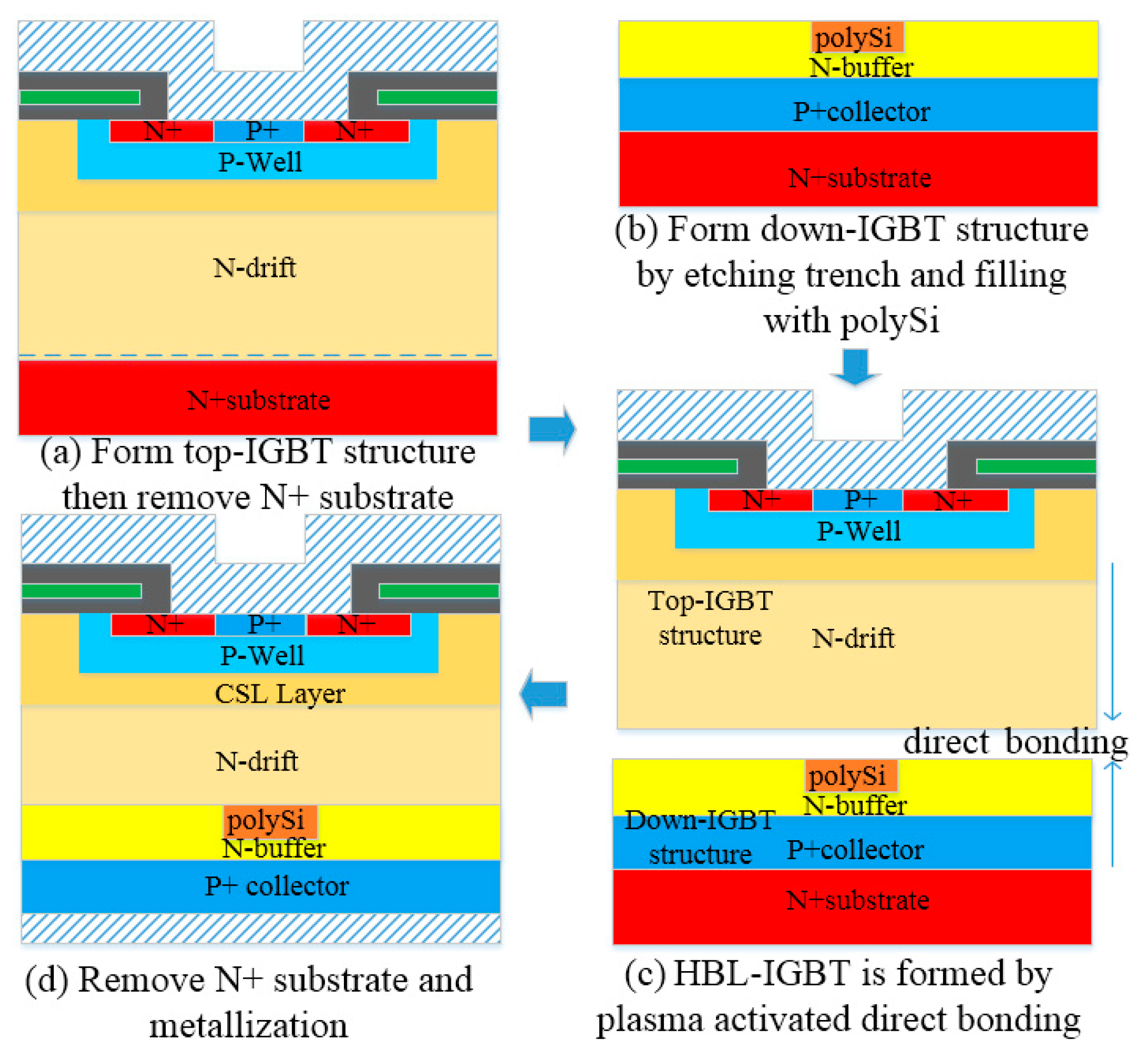
2. Device Structure and Working Mechanism

Figure 1 shows the schematic structures of a conventional IGBT (C–IGBT) and the proposed IGBT with a SiC/Si heterojunction in the buffer layer (HBL–IGBT). The parameters of both structures are provided in Table 1. The main structure parameters are the same, except for the heterojunction in the buffer layer. It is noted that three ion implantation operations are used to form a retrograde P–well, which can receive a better channel electron mobility to improve the forward voltage drop and suppress the depletion of the P–well/N–drift junction to obtain a better blocking characteristic. The electron lifetime of SiC is set to 2.5 μs, and the hole lifetime of SiC is set to 0.5 μs. The channel length is set to 1 μm, causing a channel electron mobility of 46 cm2/(V×s) and a hole mobility of 7 cm2/(V×s).
Figure 2 shows the main process flows of the HBL–IGBT. The top and down structures of the HBL–IGBT can be received. First, the top structure can grow from the N+ substrate, and the MOSFET structure of the top side is formed via ion implantation. Then, the extra N+ substrate is removed via chemical mechanical polishing (CMP). Similarly, the down structure grows from the N+ substrate. A layer of SiO2 grows as a masking layer, and the trench can be received through a lithography operation. Then, polysilicon can be formed via chemical vapor deposition (CVD). SiO2 and extra silicon are removed via chemical mechanical polishing (CMP). Finally, the heterojunction can be formed via plasma–activated direct bonding [24,25].
The thickness and width of the polySi region are denoted by TSi and WSi, respectively. The turn–off time (toff) is considered as the time from 90% VGE to 10% ICE. The time corresponding to 90% VGE is denoted by t1, and the time corresponding to 10% ICE is denoted by t2. The toff is described as
t off = t 2 t 1
The trade–off curve of the optimization of WSi and TSi between toff and the VF of a 10 A current can be seen in Figure 3. The higher VF corresponded to a worse conduction loss. From Figure 3, with increasing WSi, the VF monotonically increased, but the toff decreased. Meanwhile, the higher TSi also caused a worse VF and a better toff when the WSi was constant. It is obvious that the device performance was influenced by the polySi material parameters, because the energy bandgap of silicon is 1.12 eV, which is about one third of that of silicon carbide (3.24 eV). Thus, holes from the P+ collector and electrons from the N–drift layer can easily flood into polySi, which increases the resistance and weakens the conductivity modulation. As a result, the forward characteristic degenerates for a wider WSi and thicker TSi. At the same time, a wider WSi and thicker TSi could store more carriers when turning off, and the narrower bandgap allows excess carriers to recombine more easily compared with silicon carbide, which can restrain the current tail and provide a better toff and Eoff. Therefore, increasing TSi and WSi leads to a better turn–off characteristic. It is more beneficial to optimize polySi, which can restrain the current tail and provide a better toff and Eoff. The optimization dimensions adopted for WSi and TSi were 0.5 μm and 0.5 μm, which are appropriate sizes for etching and photolithography selection. Meanwhile, better trade–off results between the toff and VF also can be achieved, as shown in Figure 3.
The IV, blocking, and turn–off characteristics of the two structures were simulated using the Synopsys Sentaurus Technology Aided Design (TCAD) software. The key physical models for SiC power devices were adopted [26], including the Shockley–Read–Hall (SRH) model, Auger recombination model (AUGER), carrier speed saturation model (high–field saturation), incomplete ionization model, and mobility model (Lombardi). To validate the accuracy of the models used in the simulation, a structure consistent with the parameters in [27] was established, which indicated a good fitting result of the IV curves, as shown in Figure 4.
Moreover, a heterojunction interface carrier transport model was introduced because of the discontinuity in the energy band of the SiC/Si interface. The boundary conditions at the heterointerface are given by
J n , Si = v n q ( n S i n S i C exp ( Δ E C k T ) )
J p , Si = v p q ( p S i p S i C exp ( Δ E V k T ) )
where Jn,Si is the electron current density entering polysilicon, which is equal to that leaving SiC; Jp,Si is the hole current density entering polysilicon, which is equal to that leaving SiC; Δ E C is the difference between the conduction bands of the two materials; Δ E V is the difference between the valence bands of the two materials.

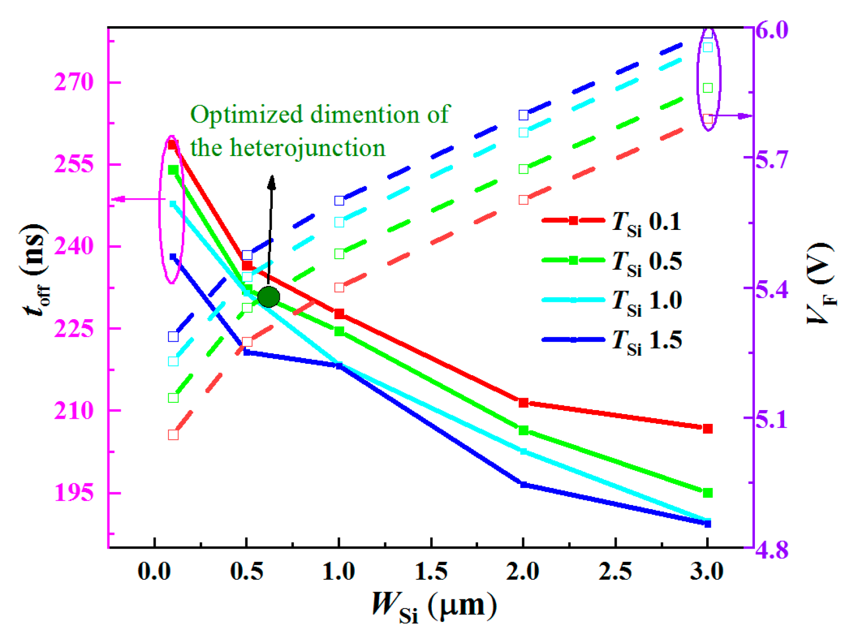
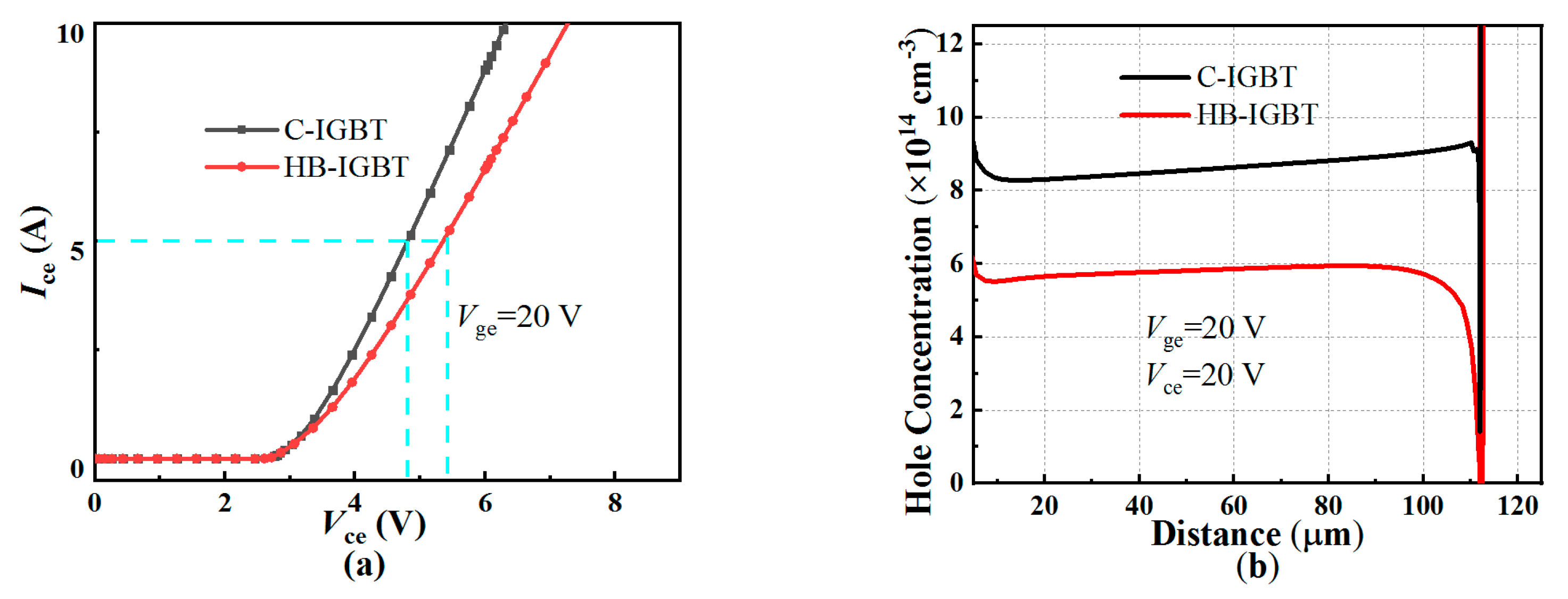
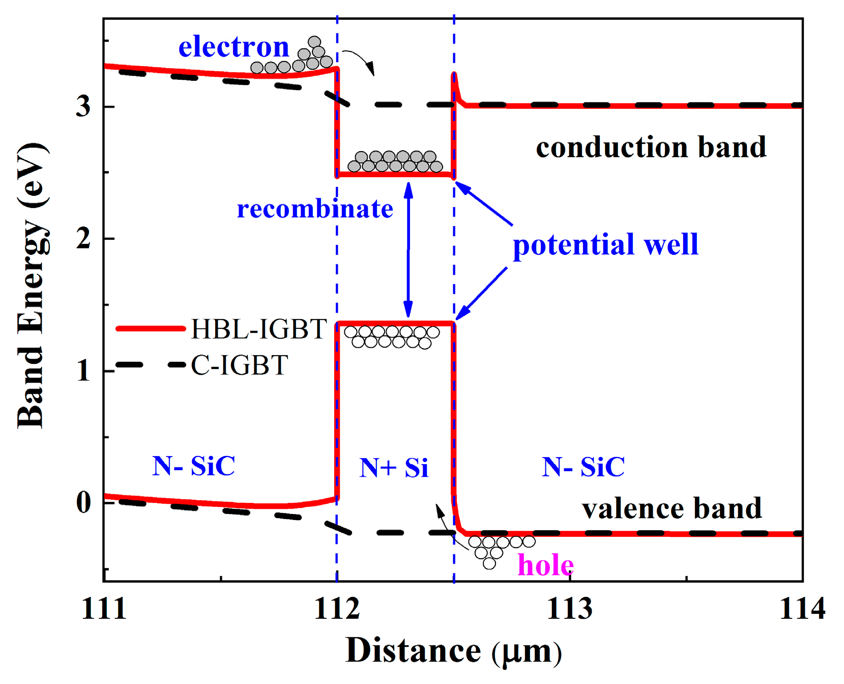
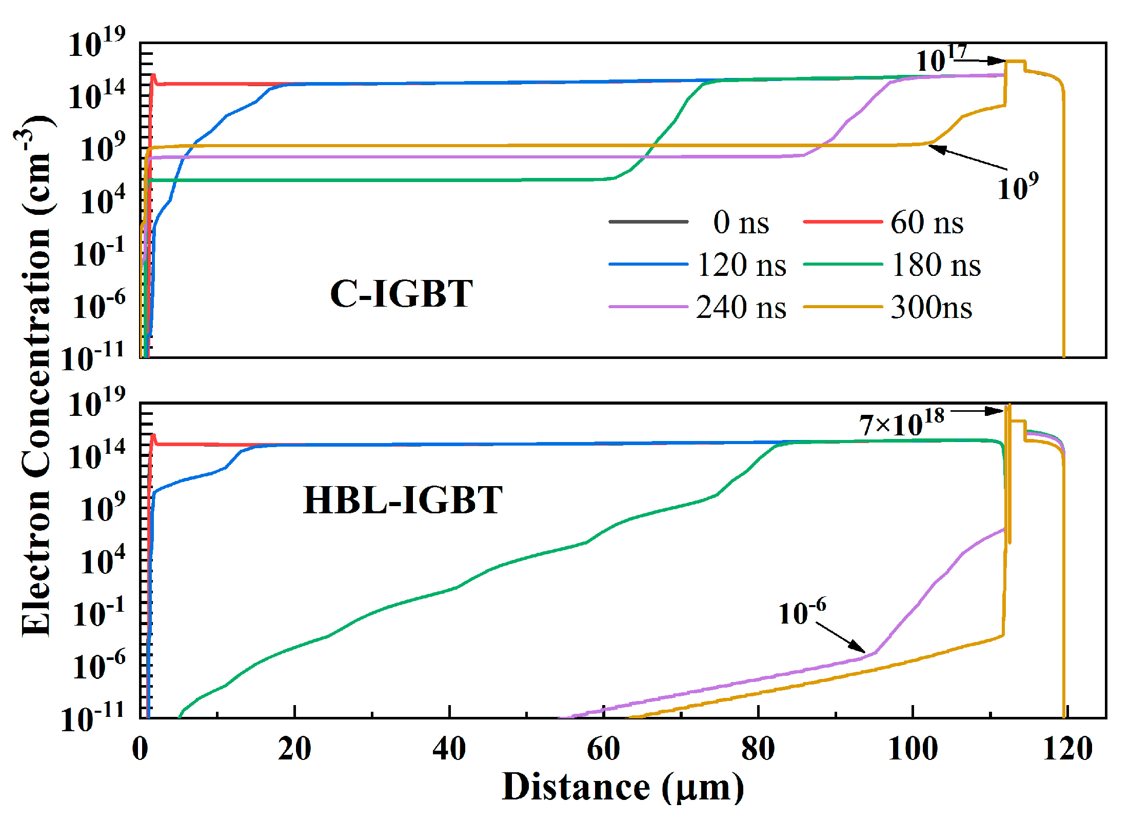
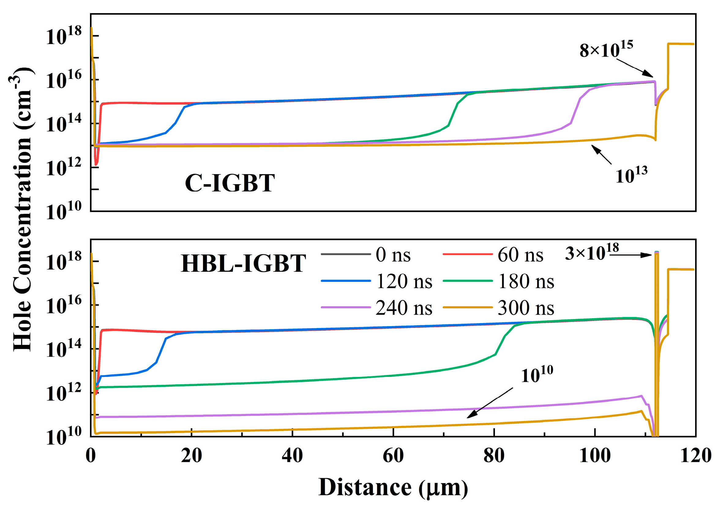
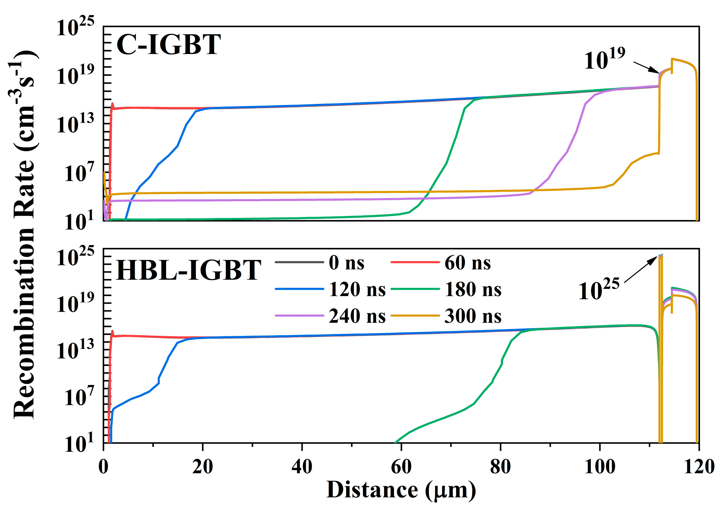
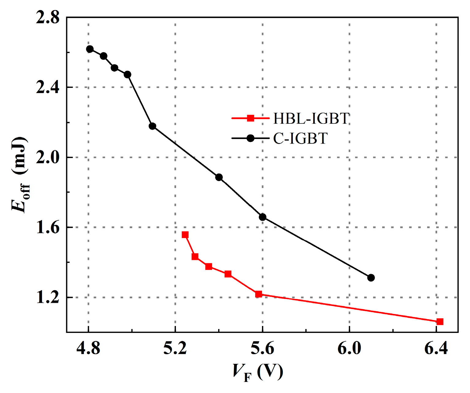
3. Simulation Results and Discussion

Figure 5a illustrates the forward IV characteristics of the C–IGBT and HBL–IGBT. It was found that the VF of C–IGBT was 4.81 V, and that of the HBL–IGBT was 5.35 V, where the HBL–IGBT exhibited a slightly higher VF. The reason is that the polySi region stores a part of the holes from the P+ collector, which reduces the hole concentration of the drift layer, as shown in Figure 5b. It can be seen that the hole concentration of the HBL–IGBT in the drift region was lower than that of the C–IGBT, resulting in degradation of the conductivity modulation.
Figure 6 presents the blocking characteristic of the C–IGBT and HBL–IGBT. The breakdown voltage of both structures approached 16 kV because of the identical parameters of the N–drift and CSL layers. Furthermore, the insert figure shows the electric field distribution of the two structures at the breakdown voltage, which shows a similar electric field distribution. The maximum electric fields in the gate oxide of the HBL–IGBT and C–IGBT were 3.31 MV/cm and 3.28 MV/cm, which are acceptable for long–term gate oxide reliability [28].
The turn–off performance of the two structures was investigated with a double–pulsed circuit, as shown in the insert of Figure 7. The bus voltage was 5 kV. The gate resistor was 10 Ω, and the gate voltage switched from 20 to 0 V. The load inductance, stray inductance, and parasitic capacitance were 3 mH, 20 nH, and 30 pF, respectively.
Figure 7 shows the simulated turn–off curves of the two structures. The turn–off loss (Eoff) is considered as the global energy during the turn–off process. The turn–off loss is described by the following equation:
E off = t 1 t 2 V C E × I C E × d t
It can be seen that the toff of the HBL–IGBT and C–IGBT was 232 ns and 325 ns, respectively. This indicates an improvement of 28.6% in the toff. The Eoff was reduced from 2.619 mJ for the C–IGBT to 1.375 mJ for the HBL–IGBT, with a reduction of about 47.5%. The main reason is that the excess carriers can flood into the polySi region due to a natural potential well in the SiC/Si heterojunction, as shown in Figure 8, resulting in an increasing carrier concentration in the polySi region. A high carrier concentration and a narrow bandgap allow electrons and holes to combine more easily, resulting in a lower toff and Eoff.
Figure 9 shows the distribution of the electron concentration of the C–IGBT and HBL–IGBT at the cutline along with the center of the device cell during the turn–off process every 60 ns steps. It can be seen that the electron concentration of the HBL–IGBT in the drift layer nearly reduced to 1 × 10⁻⁶ cm−3 at 240 ns, while the electron concentration of the C–IGBT stored in the drift layer remained at about 1 × 109 cm−3 at 300 ns. Furthermore, the maximum electron concentration was about 7 × 1018 cm−3 for the HBL–IGBT and 1 × 1017 cm−3 for the C–IGBT at 300 ns. This indicates that the huge electrons of the C–IGBT are kept in the drift layer and buffer layer, while the electrons flood into the polySi region in the HBL–IGBT during the turn–off process.
Figure 10 shows the distribution of holes during the turn–off process. It is easy to see that the hole concentration in the drift layer of the HBL–IGBT was about 1 × 1010 cm−3 at 300 ns, which was three orders of magnitude lower than that of the C–IGBT (1 × 1013 cm−3). The highest hole concentration of the HBL–IGBT was about 3 × 1018 cm−3. In the same position, that of the C–IGBT was about 8 × 1015 cm−3. Moreover, the average hole concentration of the HBL–IGBT in the drift layer was about 1011 cm−3 at 240 ns, which was much lower than that of the C–IGBT. It can be concluded that the holes accumulated in polySi in the HBL–IGBT.
The change in the recombination rate with the time variation is shown in Figure 11. The main recombination models are the SRH (Shockley–Read–Hall) recombination model and Auger recombination model, which are described by Equations (5) and (6):
R S R H = n p n i 2 τ p [ n + n i e x p ( E t r a p k T ) ] + τ n [ p + n i e x p ( E t r a p   k T ) ]
R A u g e r = ( C n n + C p p ) ( n p n i 2 )
where n is the electron concentration, p is the hole concentration, and n i is the intrinsic carrier concentration, which is related to the bandgap and temperature. Additionally, n i is constant when the bandgap and temperature do not change. It is easy to see that the electrons and holes flood into the heterojunction, which increases the carrier concentration in the polySi region. Therefore, the partial of the equation n p n i 2 increases, resulting in improvements in both SRH recombination and Auger recombination. Moreover, the bandgap of polySi is less than that of SiC, which means n i exp ( E t r a p K T ) decreases. E t r a p represents the difference between the recombination center and conduction band or valence band. Therefore, the highest recombination rate of the HBL–IGBT was more than 1025 cm−3·s−1. At the same time, the highest recombination rate of the C–IGBT was about 1019 cm−3·s−1 at the same position. It can be seen that the recombination was enhanced by the heterojunction structure during the turn–off process.
VF can be reduced and increased by changing the carrier lifetime. A higher carrier lifetime means that more holes can be injected into the N–buffer from the P+ collector, resulting in a better hole injection efficiency and leading to improvements in the conductivity modulation, obtaining a lower VF. However, higher amounts of excess carriers require more energy and time to sweep off, resulting in a higher Eoff. The trade–off relationship between the Eoff and VF is shown in Figure 12. It is shown that the HBL–IGBT presents an improved trade–off between the Eoff and VF compared with the C–IGBT, indicating a better dynamic performance.

4. Conclusions

In this paper, a novel SiC IGBT with a SiC/Si heterojunction in the buffer layer was presented and investigated by using simulation software. A heterojunction transport model was introduced and described in relation to the different bandgaps of SiC and polysilicon.
The simulation results of the new structure showed a better dynamic characteristic with a similar forward voltage ability, which was caused by the carrier storage and enhanced recombination effect in the polySi region. The performance of the proposed structure was influenced by the parameters of polysilicon; therefore, a trade–off curve of the optimization of WSi and TSi between toff and VF was drawn. The optimization dimensions adopted for WSi and TSi were 0.5 μm and 0.5 μm. For the static characteristics, the VF of the C–IGBT was 4.81 V, and that of the HBL–IGBT was 5.35 V. However, the breakdown voltage of both structures approached 16 kV. More importantly, the toff reduced from 325 ns to 232 ns, which indicated a 28.6% reduction. Additionally, the Eoff decreased from 2.619 mJ to 1.375 mJ, which indicated a 47.5% reduction. Moreover, plasma–activated direct bonding technology can be used to form the HBL–IGBT, which is compatible with the conventional process. Therefore, the HBL–IGBT is a desirable structure to optimize the performance of SiC IGBTs.

Author Contributions

Investigation, E.W. and X.T.; methodology, E.W. and X.T.; software, E.W., J.L. and C.L.; validation, E.W.; data curation, E.W.; writing—original draft preparation, E.W.; writing—review and editing, X.T., J.L., Y.B., X.L., X.W., Y.T. and C.Y.; project administration, X.T. and Y.B. All authors have read and agreed to the published version of the manuscript.

Funding

This work was supported by the High Technology Industrialization Special Fund of Cooperation between Province and Academy under Grant No. 2021SYHZ0030 and, in part, by the Key Research and Development Program of Guangdong Province under Grant 2019B090917010.

Data Availability Statement

The data presented in this study are available upon request from the corresponding author. The data are not publicly available due to privacy.

Conflicts of Interest

The authors declare no conflict of interest.

References

  1. Ballestín-Fuertes, J.; Muñoz-Cruzado-Alba, J.; Sanz-Osorio, J.F.; Laporta-Puyal, E. Role of Wide Bandgap Materials in Power Electronics for Smart Grids Applications. Electronics 2021, 10, 677. [Google Scholar] [CrossRef]
  2. Zhang, L.; Zheng, Z.; Lou, X. A Review of WBG and Si Devices Hybrid Applications. Chin. J. Electr. Eng. 2021, 7, 1–20. [Google Scholar] [CrossRef]
  3. Jain, H.; Rajawat, S.; Agrawal, P. Comparision of wide band gap semiconductors for power electronics applications. In Proceedings of the 2008 International Conference on Recent Advances in Microwave Theory and Applications, Jaipur, India, 21–24 November 2008; pp. 878–881. [Google Scholar]
  4. Iwamuro, N. Recent Progress of Power Semiconductor Devices and Their Futures. In Proceedings of the IEEE-CPMT Symposium Japan (ICSJ), Kyoto Univ Clock Tower Centennial Hall, Kyoto, Japan, 20–22 November 2017; pp. 191–194. [Google Scholar]
  5. Huang, A.Q. Power Semiconductor Devices for Smart Grid and Renewable Energy Systems. Proc. IEEE 2017, 105, 2019–2047. [Google Scholar] [CrossRef]
  6. Lorenz, L. Power Semiconductor Devices-Development Trends and System Interactions. In Proceedings of the 2007 Power Conversion Conference, Nagoya, Japan, 2–5 April 2007; pp. 348–354. [Google Scholar]
  7. Kumar, V.; Maan, A.S.; Akhtar, J. Barrier height inhomogeneities induced anomaly in thermal sensitivity of Ni/4H-SiC Schottky diode temperature sensor. J. Vac. Sci. Technol. B 2014, 32, 4. [Google Scholar] [CrossRef]
  8. Kumar, V.; Kumar, S.; Maan, A.S.; Akhtar, J. Interface improvement of epitaxial 4H-SiC based Schottky didoes by selective heavy ion irradiation. Appl. Nanosci. 2020, 13, 221–228. [Google Scholar] [CrossRef]
  9. Asada, S.; Murata, K.; Tsuchida, H. Modeling of Stacking Faults in 4H-SiC n-Type Epilayer for TCAD Simulation. IEEE Trans. Electron Devices 2023, 70, 1757–1762. [Google Scholar] [CrossRef]
  10. Madhusoodhanan, S.; Tripathi, A.; Patel, D.; Mainali, K.; Kadavelugu, A.; Hazra, S.; Bhattacharya, S.; Hatua, K. Solid-State Transformer and MV Grid Tie Applications Enabled by 15 kV SiC IGBTs and 10 kV SiC MOSFETs Based Multilevel Converters. IEEE Trans. Ind. Appl. 2015, 51, 3343–3360. [Google Scholar] [CrossRef]
  11. Iwamuro, N.; Laska, T. IGBT History, State-of-the-Art, and Future Prospects. IEEE Trans. Electron Devices 2017, 64, 741–752. [Google Scholar] [CrossRef]
  12. Tiwari, S.; Undeland, T.; Basu, S.; Robbin, W. Silicon Carbide Power Transistors, Characterization for Smart Grid Applications. In Proceedings of the 15th International Power Electronics and Motion Control Conference and Exposition (EPE-PEMC ECCE Europe), Novi Sad, Serbia, 4–6 September 2012; pp. LS6d.2-1–LS6d.2-8. [Google Scholar]
  13. Avram, M.; Brezeanu, G.; Avram, A.; Neagoe, O.; Brezeanu, M.; Iliescu, C.; Codreanu, C.; Voitincu, C. Contributions to development of high power SiC-IGBT. In Proceedings of the CAS 2005 International Semiconductor Conference, Sinaia, Romania, 3–5 October 2005; Volume 2, pp. 365–368. [Google Scholar]
  14. Ramungul, N.; Chow, T.P.; Ghezzo, M.; Kretchmer, J.; Hennessy, W. A fully planarized, 6H-SiC UMOS insulated-gate bipolar transistor. In Proceedings of the 1996 54th Annual Device Research Conference Digest, Santa Barbara, CA, USA, 26 June 1996; pp. 56–57. [Google Scholar]
  15. Han, L.; Liang, L.; Kang, Y.; Qiu, Y. A Review of SiC IGBT: Models, Fabrications, Characteristics, and Applications. IEEE Trans. Power Electron. 2021, 36, 2080–2093. [Google Scholar] [CrossRef]
  16. Kadavelugu, A.; Bhattacharya, S.; Ryu, S.; Brunt, E.V.; Grider, D.; Agarwal, A.; Leslie, S. Characterization of 15 kV SiC n-IGBT and its application considerations for high power converters. In Proceedings of the 2013 IEEE Energy Conversion Congress and Exposition, Denver, CO, USA, 15–19 September 2012; pp. 2528–2535. [Google Scholar]
  17. Van Brunt, E.; Cheng, L.; O’Loughlin, M.J.; Richmond, J.; Pala, V.; Palmour, J.W.; Tipton, C.W.; Scozzie, C. 27 kV, 20 A 4H-SiC n-IGBTs. Mater. Sci. Forum 2015, 821–823, 847–850. [Google Scholar] [CrossRef]
  18. Johannesson, D.; Nawaz, M.; Norrga, S.; Hallen, A.; Nee, H.-P. Static and Dynamic Performance Prediction of Ultrahigh-Voltage Silicon Carbide Insulated-Gate Bipolar Transistors. IEEE Trans. Power Electron. 2021, 36, 5874–5891. [Google Scholar] [CrossRef]
  19. Zhang, J.; Luo, J.; Chen, Z.; Li, Z.; Zhang, B. A Novel Snapback-Free Reverse-Conducting IGBT with Si/SiC Heterojunction. In Proceedings of the IEEE Electron Devices Technology and Manufacturing Conference (EDTM), Penang, Malaysia, 6–21 April 2020; pp. 1–4. [Google Scholar]
  20. Yu, H.; Liang, S.; Liu, H.; Wang, J.; Shen, Z.J. Numerical Study of SiC MOSFET With Integrated n-/n-Type Poly-Si/SiC Heterojunction Freewheeling Diode. IEEE Trans. Electron Devices 2021, 68, 4571–4576. [Google Scholar] [CrossRef]
  21. Wang, Y.; Yu, C.-H.; Mao, H.-K.; Wu, X.; Su, F.-W.; Li, X.-J.; Yang, J.-Q. Low Turn-Off Loss 4H-SiC Insulated Gate Bipolar Transistor with a Trench Heterojunction Collector. IEEE J. Electron Devices Soc. 2020, 8, 1010–1015. [Google Scholar] [CrossRef]
  22. Liu, Y.-J.; Wang, Y.; Hao, Y.; Yu, C.-H.; Cao, F. 4H-SiC Trench IGBT With Back-Side n-p-n Collector for Low Turn-OFF Loss. IEEE Trans. Electron Devices 2017, 64, 488–493. [Google Scholar] [CrossRef]
  23. Synopsys TCAD Tools; Synopsys: Mountain View, CA, USA; Available online: http://www.synopsys.com (accessed on 1 January 2013).
  24. Mu, F.; Iguchi, K.; Nakazawa, H.; Takahashi, Y.; Fujino, M.; He, R.; Suga, T. A comparison study: Direct wafer bonding of SiC–SiC by standard surface-activated bonding and modified surface-activated bonding with Si-containing Ar ion beam. Appl. Phys. Express 2016, 9, 081302. [Google Scholar] [CrossRef]
  25. Kang, Q.; Wang, C.; Niu, F.; Zhou, S.; Xu, J.; Tian, Y. Single-crystalline SiC integrated onto Si-based substrates via plasma-activated direct bonding. Ceram. Int. 2020, 46, 22718–22726. [Google Scholar] [CrossRef]
  26. Hatakeyama, T.; Fukuda, K.; Okumura, H. Physical Models for SiC and Their Application to Device Simulations of SiC Insulated-Gate Bipolar Transistors. IEEE Trans. Electron Devices 2013, 60, 613–621. [Google Scholar] [CrossRef]
  27. Fukuda, K.; Okamoto, D.; Okamoto, M.; Deguchi, T.; Mizushima, T.; Takenaka, K.; Fujisawa, H.; Harada, S.; Tanaka, Y.; Yonezawa, Y.; et al. Development of Ultrahigh-Voltage SiC Devices. IEEE Trans. Electron Devices 2015, 62, 396–404. [Google Scholar] [CrossRef]
  28. Cooper, J.A.; Morisette, D.T.; Sampath, M.; Stellman, C.A.; Bayne, S.B.; Westphal, M.J.; Anderson, C.H.; Ransom, J.A. Demonstration of Constant-Gate-Charge Scaling to Increase the Robustness of Silicon Carbide Power MOSFETs. IEEE Trans. Electron Devices 2021, 68, 4577–4581. [Google Scholar] [CrossRef]
Figure 1. Schematic structures of (a) C–IGBT and (b) HBL–IGBT.
Electronics 12 02501 g001
Figure 2. Main fabrication steps of the HBL–IGBT structure.
Electronics 12 02501 g002
Figure 3. The optimization of TSi and WSi between the VF and toff of the HBL–IGBT.
Electronics 12 02501 g003
Figure 4. Comparison of the on–state characteristics of the SiC IGBT simulation and measurement.
Electronics 12 02501 g004
Figure 5. Two structures of the (a) simulated on–state curve and (b) hole concentration in the cutline in the center of the cell.
Electronics 12 02501 g005
Figure 6. Breakdown characteristic curves and electric fields of (a) C–IGBT and (b) HBL–IGBT.
Electronics 12 02501 g006
Figure 7. Comparison of turn–off curves between C–IGBT and HBL–IGBT.
Electronics 12 02501 g007
Figure 8. Comparison of energy band diagrams between HBL–IGBT and C–IGBT with the cutline in the center of the cell.
Electronics 12 02501 g008
Figure 9. The distribution of the electron concentration during the turn–off process.
Electronics 12 02501 g009
Figure 10. The distribution of the hole concentration during the turn–off process.
Electronics 12 02501 g010
Figure 11. The distribution of the recombination rate during the turn–off process.
Electronics 12 02501 g011
Figure 12. The trade–off relationship between the Eoff and VF.
Electronics 12 02501 g012
Table 1. Detailed structure parameters of the two SiC IGBTs.
ParametersC–IGBTHBL–IGBT
Cell pitch (μm)1515
Active area (mm2)1616
P+ collector depth (μm)55
P+ collector doping (cm−3)1 × 10191 × 1019
Gate oxide thickness (nm)6060
N–CSL doping (cm−3)8 × 10158 × 1015
N–CSL thickness (μm)22
N–drift thickness (μm)110110
N–drift doping (cm−3)4 × 10144 × 1014
N–buffer thickness (μm)2.52.5
N–buffer doping (cm−3)2 × 10172 × 1017
N+ polysilicon doping (cm−3)--1 × 10¹⁹
Trench heterojunction thickness (μm)--0.5
Trench heterojunction width (μm)--0.5
Disclaimer/Publisher’s Note: The statements, opinions and data contained in all publications are solely those of the individual author(s) and contributor(s) and not of MDPI and/or the editor(s). MDPI and/or the editor(s) disclaim responsibility for any injury to people or property resulting from any ideas, methods, instructions or products referred to in the content.

