Article

Total Ionizing Dose Effects of 60Co γ-Ray Radiation on Split-Gate SiC MOSFETs

1
Key Laboratory of Functional Materials and Devices for Special Environments of CAS, Xinjiang Key Laboratory of Electric Information Materials and Devices, Xinjiang Technical Institute of Physics and Chemistry of CAS, Urumqi 830011, China
2
University of Chinese Academy of Sciences, Beijing 100049, China
3
State Key Laboratory of Wide-Band Gap Semicond, Nanjing Electronic Devices Institute, Nanjing 210016, China
*
Authors to whom correspondence should be addressed.
Electronics 2023, 12(11), 2398; https://doi.org/10.3390/electronics12112398
Submission received: 24 April 2023 / Revised: 19 May 2023 / Accepted: 19 May 2023 / Published: 25 May 2023
(This article belongs to the Special Issue Radiation Effects of Advanced Electronic Devices and Circuits)

Abstract

:
SiC power devices require resistance to both single-event effects (SEEs) and total ionizing dose effects (TIDs) in a space radiation environment. The split-gate-enhanced VDMOSFET (SGE-VDMOSFET) process can effectively enhance the radiation resistance of SiC VDMOS, but it has a certain impact on the gate oxide reliability of SiC VDMOS. This paper investigates the impact mechanism and regularity of using the SGE process to determine the radiation resistance and long-term reliability of SiC VDMOS under other identical processes and radiation conditions. Our experimental results show that after 60Co γ-ray irradiation, the degradation degrees of the static parameters of SGE-VDMOSFET and planar gate VDMOSFET (PG-VDMOSFET) are similar. The use of the new process leads to more defects in the oxide layer, reducing the long-term reliability of the device, but its stability can recover after high-temperature (HT) accelerated annealing. This research indicates that enhancing the resistance of SEEs using an SGE-VDMOSFET structure requires simultaneously considering the demand for TIDs and long-term reliability.

1. Introduction

As the aerospace industry rapidly develops towards deep space exploration, electronic devices are facing increasingly diverse working environments, making it particularly important to ensure the stability of device operation in complex space environments. A space radiation environment is filled with a large number of high-energy particles such as electrons, protons, gamma-rays, and heavy ions, which pose a threat to semiconductor components in spacecrafts [1,2]. Silicon carbide power field effect transistors (SiC VDMOS) have significant advantages, including high temperature, high power, high efficiency, and reduced volume, meeting the requirements of the new generation of spacecraft power semiconductor devices. Therefore, SiC-based power semiconductor devices have great potential for application in space radiation environments [3,4].
Currently, the radiation effects of SiC metal-oxide semiconductor field-effect transistors (SiC MOSFETs) have gained attention [5,6,7,8]. In 2012, Akturk et al. conducted a TID experiment on 1200 V SiC MOSFET power devices using 60Co γ-radiation. The results showed that the device still had good performance when the accumulated dose exceeded 100 krad (Si). When the accumulated dose exceeded 300 krad (Si), the capacitance between the gate and drain changed, which significantly affected the device’s switching performance [9]. In 2014, Alexandru et al. examined the influence of proton and electron irradiation on the electrical parameters of 4H-SiC nMOSFETs [10]. The results showed that the threshold voltage decreased after proton irradiation and tended to stabilize over time. With an increase in proton dose, the threshold voltage showed a decreasing trend. Similar changes were observed before and after electron irradiation. Meanwhile, the gate leakage current remained almost unchanged under the highest flux proton irradiation and the maximum dose of electron irradiation [11]. In 2019, TID radiation experiments were conducted on different SiC power devices by Hazdra and Popelka. The results showed that SiC devices with an oxide layer were more susceptible to TIDs after radiation [12].
In recent years, the radiation damage effects and radiation hardening techniques of SiC VDMOS devices have gradually become a research hotspot due to their sensitivity to radiation-induced damage in the oxide layer. Among them, the function disablement characteristic of SEE radiation damage has received extensive attention both domestically and abroad [13,14,15,16]. Increasing the thickness of the VDMOS oxide layer is a commonly employed measure to strengthen resistance against SEEs. This method can effectively enhance the device’s resistance to single-Event gate rupture (SEGR) and has already been extensively studied in silicon-based VDMOS. As early as 1986, A. E. Waskiewicz et al. first proposed the SEB effect of power VDMOS devices [17]. In 1987, T. Fischer proposed the SEGR effect of power VDMOS devices [18]. Cascio, A et al. proposed a method of thickening the gate dielectric, where they reinforced the device by separately depositing a thick oxide layer in the gate oxide region of the JFET region. The purpose of this structure is to increase the breakdown voltage of the gate dielectric layer by increasing the thickness of the oxide dielectric layer, thereby improving the device’s resistance to SEEs [19]. The LOCOS (Local Oxidation of Silicon) structure adopted by Tang Zhaohuan and colleagues is also a reinforcement measure based on the principle of thickening the gate oxide layer. However, unlike the method of depositing a thick gate oxide layer alone, this structure consumes some of the silicon thickness in the JFET region [20]. Currently, conventional reinforcement technology improves the SEE resistance in power MOSFET, which can result in performance loss to factors such as conductivity and reliability. Therefore, determining how to improve SEE resistance while meeting the basic operating characteristics of the device has long been a focus of research for experts in radiation hardening.
Specific on-resistance (Ronsp) is an important indicator for evaluating the performance of unipolar power devices. Its physical meaning is the product of the on-resistance of the device and the active conducting area of the chip. A smaller value indicates a higher technical level, meaning that products with the same on-resistance value require smaller chip areas. In 1993, J.W. Palmour proposed a vertical UMOSFET structure based on an immature ion implantation process in a silicon carbide material. As a result, this structure eliminated lattice loss caused by ion implantation through epitaxy, enabling the device to withstand voltages up to 330 V with a Ronsp of 33 mΩcm2. Due to various issues in the UMOS structure process, more researchers have focused on research on VDMOS devices in recent years. However, VDMOS devices have a large gate-drain capacitance, which greatly reduces their frequency response and performance when the device operates under a high-frequency state, leading to performance losses [21,22]. To optimize the working performance of VDMOS devices under high-frequency conditions, the split-gate structure (split gate) emerged as a solution, dividing the gate structure in two. This structure significantly reduced gate leakage capacitance and improved the performance of trench-gate VDMOS devices.
Modifying the oxide layer structure of VDMOS can effectively enhance the radiation tolerance of SiC VDMOS, but this complex process could potentially affect the reliability of the gate oxide. With the use of a new split-gate structure oxide process, defects of different types and spatial distributions will occur inside the gate oxide layer, which will affect the TID sensitivity of SiC VDMOS. Therefore, investigating the quality of the oxide layer of the split-gate structure and studying the changes in TID radiation damage are crucial.
This paper presents a comparative study on the TID sensitivity and long-term reliability of the traditional PG-VDMOSFET structure and the SG-VDMOSFET structure. The transfer characteristics curves (IDSVGS), threshold voltage drift (ΔVTH), on-resistance (RDS(on)), leakage current (IGSS), interface state density (Nit), and current density–electric field strength characteristic curves (J-E characteristic curves) were analyzed before and after radiation exposure. This research is based on the improvement of electrical parameters and reliability degradation of SiC VDMOS, providing experimental data to optimize the gate oxide process and mitigate TID damage for SiC VDMOS.

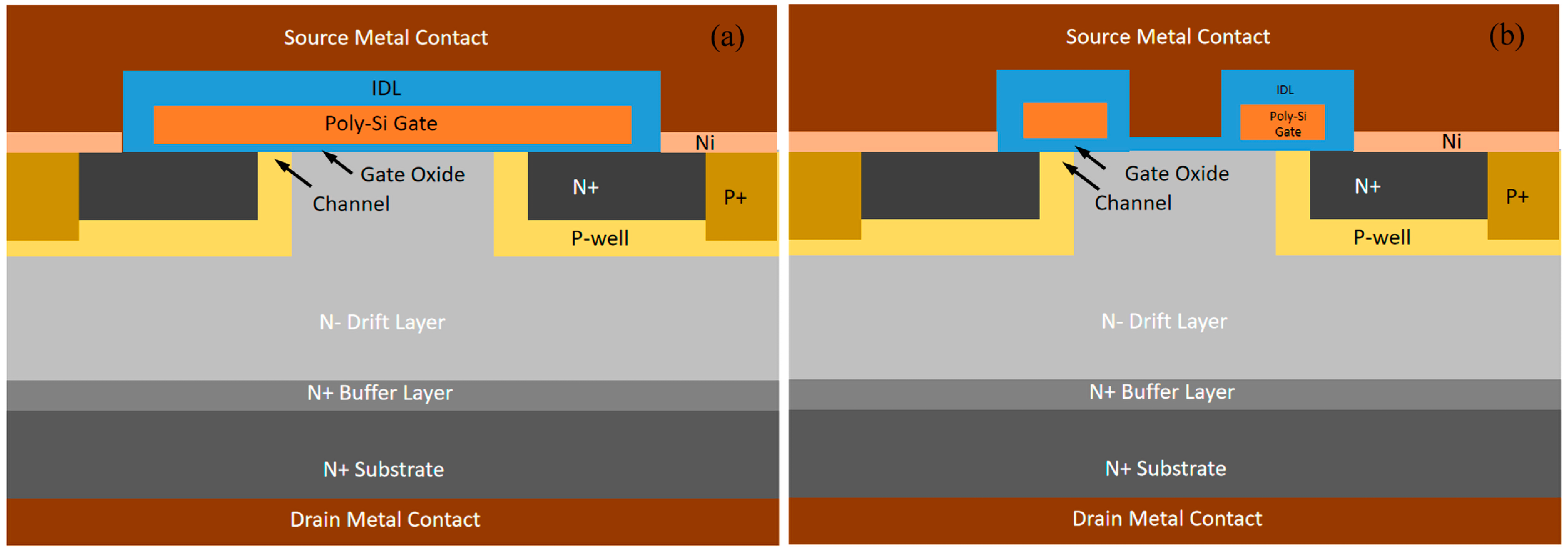
2. Samples and Experimental Setup

This experiment utilized two domestically produced 1200 V N-channel SiC VDMOS devices with a planar gate structure, both packaged in TO-247-3 packages and processed using the same process flow. P-type wells and N+ source regions were doped via ion implantation on a 10 um epitaxial layer to form the MOSFET channel region. The gate oxide layer was then grown via thermal oxidation and annealed in a NO atmosphere after a HT treatment to activate the carriers. The two devices featured the same cell structure and had a tox of 50 nm. Specifically, the split-gate structure SiC VDMOS has two symmetrical gate electrodes placed at an interval on top of the gate insulation layer, with a single gate length of 1.2–1.25 um and a distance of 1.3 um between the two gates. Figure 1 shows the schematic of two different structures of VDMOSFETs: (a) SGE-VDMOSFET; (b) PG-VDMOSFET.
The experiment was carried out at the Xinjiang Institute of Physics and Chemistry, Chinese Academy of Sciences. The irradiation source was 60Co, and the dose rate was 100 rad (Si)/s. The samples were irradiated to 300 krad (Si) with a positive gate bias (VGS = 20 V, drain and source grounded) at room temperature (RT).
An Agilent B1500 A semiconductor device analyzer was used to measure the IDSVGS curve before irradiation. Linear extrapolation was performed on the IDSVGS curve to obtain the threshold voltage (VTH) of the device. The RDS (on) was tested using a semiconductor isolation device testing system (BC3193) based on the device datasheet, and IGSS was tested at VGS =20 V and VDS = 0 V. Some devices were subjected to TID irradiation followed by 168 h annealing at 100 °C, with the same bias as the radiation process maintained on all pins. The device characteristics were then retested after annealing.

3. Results and Analyses

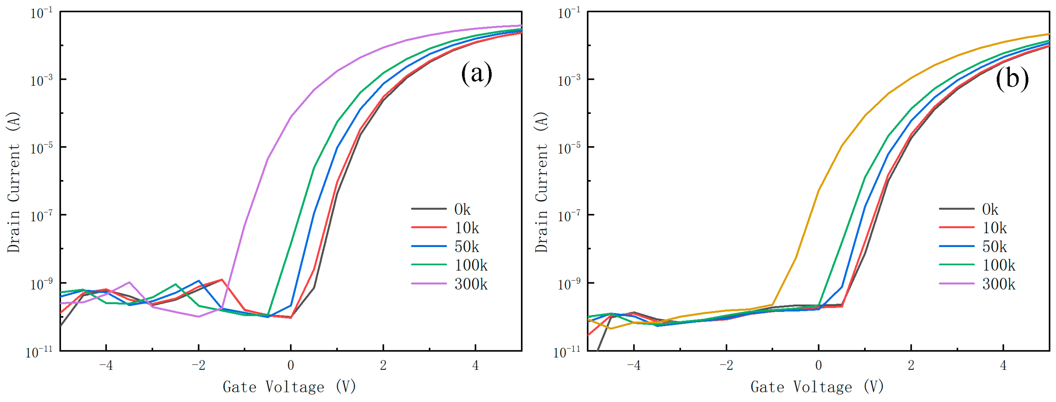
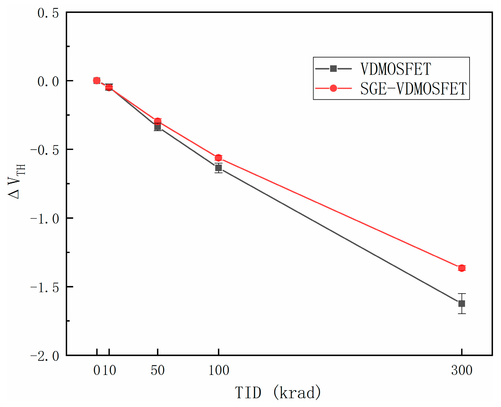
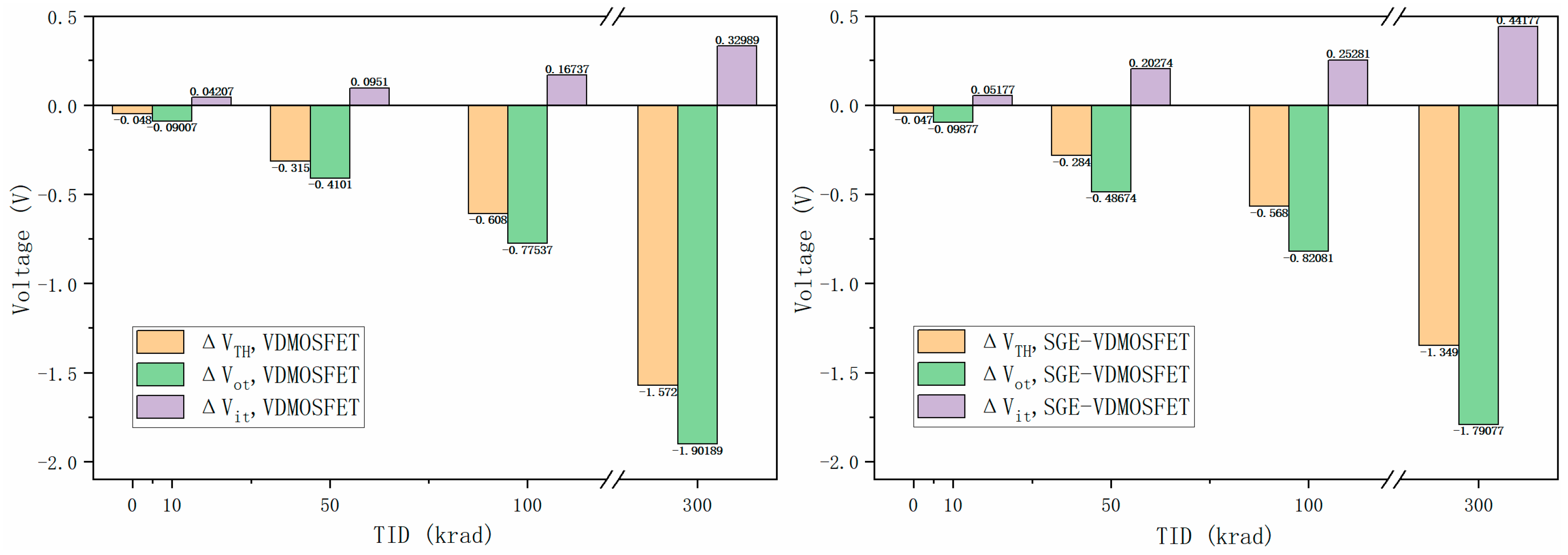
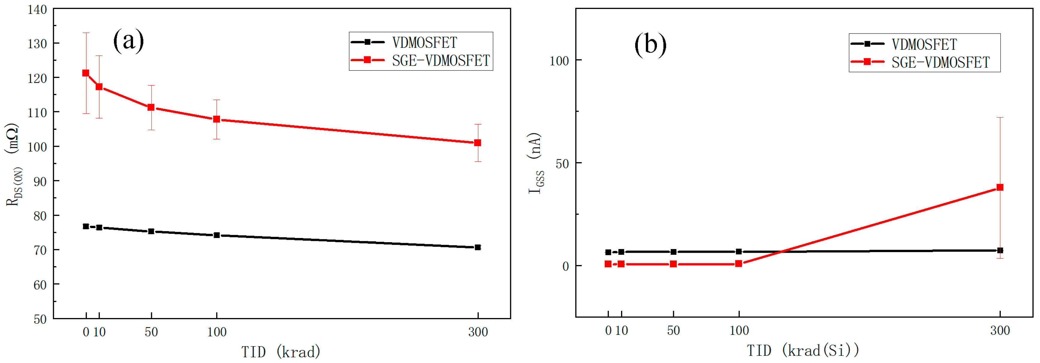
3.1. The Influence of TID Radiation on the Static Characteristics of SGE-VDMOSFET and PG-VDMOSFET

Figure 2 shows the relationship between the IDSVGS curves and cumulative dose for the two types of SiC VDMOS transistor. For the IDSVGS curve, we mainly focus on its sub-threshold region, so the size of VD does not affect the area we need to observe. At the same time, when testing the IDSVGS curve using the Agilent B1500 A semiconductor device analyzer, if VD is greater than 0.1 V and the device is conducting, the equipment will cause current limiting and cannot be tested. Therefore, to obtain the complete IDSVGS curve of the device, VD needs to be set to less than or equal to 0.1 V. As the same process and cell size were used, the investigation of TIDs was mainly focused on the oxide thickness (tox) of the devices. In terms of radiation damage, the SGE-VDMOSFET exhibited less severe damage than the PG-VDMOSFET. Figure 3 shows the threshold voltage degradation curves of the two devices, with good consistency observed among multiple tested devices in terms of threshold voltage performance. As the cumulative dose increased, the threshold voltage decreased uniformly for both devices. The threshold voltage of the PG-VDMOSFET had a negative drift of 1.62 V at a cumulative dose of 300 krad (Si), while the SGE-VDMOSFET already exhibited a threshold voltage drift of 1.36 V at the same cumulative dose.
Radiation causes ionization in the gate oxide, resulting in the generation of a large number of electron–hole pairs. Although there are a small number of electron traps formed by carbon residues during the thermal oxidation growth process in the gate oxide, their density is extremely low, and the electrons with high mobility will be quickly swept out of the gate oxide layer under the influence of an electric field. The holes with lower mobility are more likely to be captured by hole traps in the oxide layer, becoming positively charged oxide traps. Oxide traps (mainly hole traps generated during the thermal oxidation process) will capture more positively charged holes after irradiation, leading to an increased inversion degree of the NMOS channel and a negative shift in the transfer characteristic curve towards the negative x-axis. The oxide trap charges that affect the threshold voltage of the device are mainly located above the channel, with a smaller influence on the gate oxide layer in the JFET region. Therefore, theoretically, under the same gate oxide thickness for both devices, the degradation of the threshold voltage should be almost the same. However, it can be clearly seen from the data of multiple devices that the threshold voltage degradation of the SGE-VDMOSFET is weaker. This phenomenon often occurs due to defects in the interface between the gate oxide layer and the silicon carbide substrate caused by changes in the gate oxide layer fabrication process. Therefore, in Section 3.2 of this article, this inference is validated.
Subthreshold Swing (SS) refers to the change in IDS with a one-decade increase in VGS. It represents the change in gate voltage required for the IDS to vary by a factor of 10 and is also known as the S factor. A smaller S value indicates a faster ON/OFF switching speed.
S = d V G S d ( lg I D S ) = ln 10 d V G S d ( ln I D S ) = ln 10 d ψ s d I D S I D S d V G S d ψ s
d ψ s d I D S I D S = k T q
η = d V G S d ψ s = C o x + C d e p + C i t C o x
SS = k T q η ln 10 = k T q C o x + C d e p + C i t C o x ln 10
In this equation, K T q represents the thermal voltage, η is referred to as the body factor, and ψ s is the surface potential. C o x is the capacitance of the top-gate oxide layer, C d e p is the depletion capacitance, C i t is the interface trap capacitance, k is the Boltzmann constant, T is the temperature, and q is the electronic charge.
The factors affecting subthreshold swing are as follows: (1) An increase in temperature leads to an increase in subthreshold swing. (2) An increase in gate oxide capacitance leads to a decrease in subthreshold swing; the use of high-k dielectric materials or a reduction in the gate oxide thickness can result in a decrease in subthreshold swing. (3) A decrease in Si depletion layer capacitance results in a decrease in subthreshold swing; factors that may increase the depletion layer width, such as a decrease in substrate concentration Na or an increase in substrate bias voltage, lower the subthreshold swing. (4) Interface defects between the gate oxide layer and the substrate silicon can store charge and can effectively increase the capacitance, leading to an increase in the subthreshold swing. (5) A shorter channel length weakens the gate control capability, and hence, leads to an increase in subthreshold swing. (6) An increase in gate voltage results in stronger surface inversion, leading to weaker gate control of the channel and an increase in subthreshold swing.
Figure 4 shows the relationship between the S and the total irradiation dose for the two SiC VDMOS transistors. After TID radiation, the S value of the SGE-VDMOSFET changes slightly from 282 to 301, while the S of the PG-VDMOSFET remains almost unchanged.

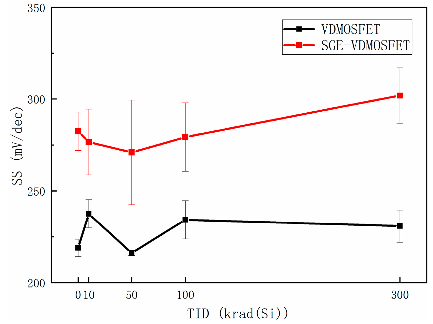
3.2. Differences in Threshold Voltage Degradation between SGE-VDMOSFET and PG-VDMOSFET

According to possible charge states, interface states are divided into acceptor-type interface states and donor-type interface states. Regarding acceptor-type interface traps, they are negatively charged when they are filled with electrons and electrically neutral when electrons are lost. For donor-type interface states, they are electrically neutral when they are filled with electrons and positively charged when electrons are lost. When the Fermi level at the interface coincides with the center of the bandgap (mid-gap), the interface states are approximately electrically neutral, and do not cause mid-gap voltage changes. Since the distribution of interface states in the bandgap is complex, it can only be assumed that the interface states are approximately electrically neutral at the mid-gap. Other factors affecting threshold voltage, such as work function difference and semiconductor space charge, do not change due to irradiation; therefore, the change in mid-gap voltage caused by irradiation is mainly due to the change in oxide trap charge [23,24,25].
Figure 5 shows the voltage changes caused by oxide trap charge-induced changes (ΔVot) and interface state-induced changes (ΔVit) as separated using the mid-gap voltage method [26]. It can be seen that ΔVot is the main cause of the threshold voltage change. During the thermal oxidation process, the oxide layer hole traps generated by oxygen defects and the near-interface hole traps formed during nitrogen passivation can capture a large number of holes generated via ionizing radiation. The trapped holes mainly affect the threshold voltage drift of the device. After being exposed to total ionizing radiation, the ΔVTH of PG-VDMOSFET decreased by 1.6 V, and the ΔVTH of SGE-VDMOSFET decreased by 1.4 V, with weaker degradation in the ΔVTH of SGE-VDMOSFET. The ΔVot of PG-VDMOSFET decreased by 1.9 V, and the ΔVot of SGE-VDMOSFET decreased by 1.8 V, with weaker degradation in the ΔVot of SGE-VDMOSFET. The ΔVit of PG-VDMOSFET increased by 0.3 V, and the ΔVit of SGE-VDMOSFET increased by 0.4 V, with stronger degradation in the ΔVit of SGE-VDMOSFET. Our analysis indicates that there are two reasons for the weaker degradation in the ΔVTH of SGE-VDMOSFET: (1) from the ΔVot perspective, the SGE-VDMOSFET utilizing the new process has fewer oxide defect potential hole traps in the oxide layer produced during the thermal oxidation process compared to PG-VDMOSFET, leading to weaker degradation in the ΔVot of SGE-VDMOSFET; (2) from the ΔVit perspective, PG-VDMOSFET has fewer interface states at the gate oxide interface due to less etching, resulting in fewer captured electrons during the radiation process and weaker degradation in the ΔVit. Overall, reason 2 is the main reason for the weaker degradation in the ΔVTH of SGE-VDMOSFET.
When designing a switching power supply or driving circuit using MOSFET, it is generally necessary to consider the on-resistance of the MOSFET. Because energy is consumed on this resistance when current flows through the drain and source, this energy consumption is called conduction loss. Choosing a MOSFET with a lower on-resistance can reduce conduction loss to a certain extent. If a higher breakdown voltage is required, the internal structure needs to be made thicker, so the on-resistance of a MOSFET with a higher breakdown voltage will be larger.
Meanwhile, gate leakage current is also a very important parameter in semiconductor devices. It describes the insulation effect of the transistor and has an important impact on the service life and stability of the device. The gate leakage current refers to the leakage current between the gate and drain of a transistor when it is in the off state. By measuring the leakage current value of the device, we can evaluate the insulation quality. As an important component of semiconductor devices, the gate leakage current of a transistor has a significant impact on its performance.
There are three factors that affect gate leakage current: 1. Temperature is an important factor that affects gate leakage current. As the temperature increases, the leakage current between the gate and drain of the transistor gradually increases. Therefore, when conducting temperature tests, it is necessary to ensure that the operating temperature of the transistor does not exceed its allowable maximum temperature. At the same time, it is also necessary to compare different devices under the same temperature conditions to determine the magnitude of their gate leakage current. 2. Voltage is also one of the factors that affect the magnitude of the transistor’s gate leakage current. At a certain operating temperature, as the acceleration voltage increases, the gate leakage current of the transistor also shows an increasing trend. Therefore, when conducting gate leakage current tests, attention should be paid to the selection of the test voltage and the duration of the test. 3. The quality of insulation materials also affects the magnitude of the gate leakage current. Higher-quality insulation materials can effectively suppress the gate leakage current of the transistor. Therefore, when designing semiconductor devices, it is necessary to select high-quality insulation materials to ensure the stability and reliability of the device.
Figure 6 shows the changes in the electrical parameters of two SiC VDMOS transistors as a function of accumulated radiation dose. After irradiation, the gate oxide of the two devices accumulated positive charges in oxide traps to varying degrees. Defects that carry a positive charge attract electrons onto the semiconductor surface, increasing the surface electron concentration, and hence, reducing the device RDS (on). When the accumulated dose reaches 300 krad (Si), the IGSS of SGE-VDMOSFET increases slightly but remains at the nA level. TIDs do not significantly affect the IGSS of either device. The examination of gate leakage current is often carried out by observing whether it undergoes a sudden change from the nA level to the μA level. The variation in Figure 6 is very small, which is highly likely to be due to measurement errors caused by the equipment.

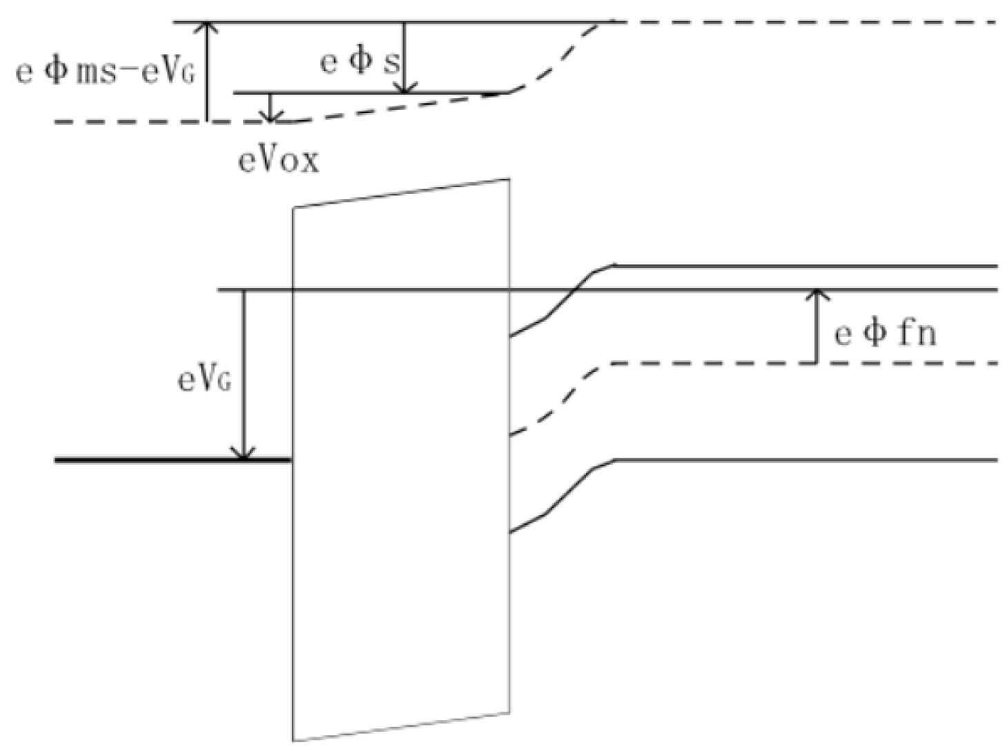
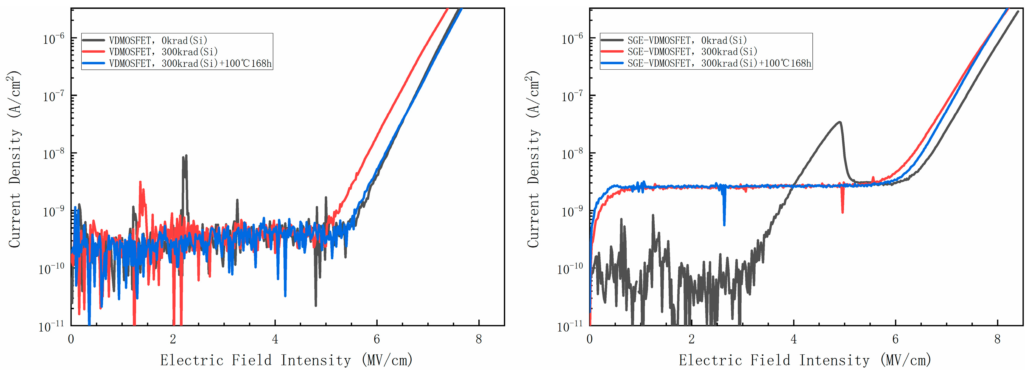
3.3. The Influence of TID Radiation on Electron Tunneling in Gate Oxide

It is generally accepted that Fowler–Nordheim (F-N) tunneling becomes one of the main reasons for charge transport through the oxide layer when the oxide layer is thick or the gate voltage is high. F-N tunneling is an electron tunneling phenomenon caused by an electric field. As shown in Figure 7, when a high voltage is applied to the polycrystalline silicon/oxide/carbon structure, the barrier in the oxide layer becomes very steep, and electrons in the SiC conduction band face a triangular barrier that depends on the external electric field. When the voltage is high enough, the barrier becomes extremely narrow, and electrons can tunnel through the barrier, entering the oxide conduction band from the SiC conduction band, thus inducing F-N tunneling. The tunneling current density can be expressed as follows using a self-consistent electron model and WKB approximation [27]:
J F N = q 3 E 2 16 π ħ ϕ B exp ( 4 2 m * ϕ B 3 3 q ħ E )
The expression can be adjusted using a correction factor that includes as the reduced Planck constant, ϕ B as the barrier height, m * as the effective mass of electrons in the oxide layer, and E as the electric field strength in the oxide layer. The correction factor can reflect the effect of the mirror potential as well as the influence of temperature on the tunneling process [28].
Figure 8 shows changes in the gate oxide J-E curves of two SiC VDMOS transistors as a function of accumulated total dose. For the PG-VDMOSFET device, the gate oxide current density increases uniformly when the accumulated dose reaches 300 krad (Si), but the characteristic gradually recovers after 168 h HT accelerated annealing. The J-E characteristic of non-irradiated SGE-VDMOSFET exhibits hysteresis at an electric field strength of 4 MV/cm. When the accumulated dose for SGE-VDMOSFET reaches 300 krad (Si), the tunneling characteristic of the device tends to be stable, and the device has better gate oxide characteristics after subsequent 168 h HT accelerated annealing. Further investigation is required to ensure the long-term reliability of the device.

4. Conclusions

With an increase in accumulated dose during 60Co γ-ray irradiation, both PG-VDMOSFET and SGE-VDMOSFET experience varying degrees of radiation damage. For VTH, SGE-VDMOSFET experiences weaker degradation compared to PG-VDMOSFET. This is mainly due to the presence of more defects at the interface during the growth and etching of gate oxide in SGE-VDMOSFET, and an increase in interface states after irradiation. The electrical performance consistency of SGE-VDMOSFET devices is poor. At the same time, there are reliability problems with the gate oxide. The initial samples had more deep-level defects inside the gate oxide, which facilitated electron tunneling from the substrate through F-N tunneling under electric stress. The SGE process may lead to the generation of more deep-level defects in the gate oxide when solving the SEE problems of SiC VDMOS. J-E can be significantly improved after irradiation and 168 h high-temperature annealing. Improving the SEE resistance of SiC VDMOS via the SGE process requires consideration of the long-term reliability degradation of the devices.

Author Contributions

Conceptualization, H.F. and X.Y.; methodology, H.F., X.P., D.Z. and X.Y.; software, Y.X. and Y.W.; validation, H.F.; formal analysis, H.F.; investigation, H.F. and X.P.; resources, T.Z.; data curation, X.L.; writing—original draft preparation, H.F.; writing—review and editing, H.F., X.Y. and Q.G.; visualization, H.F.; supervision, X.L. and X.Y.; project administration, X.Y.; funding acquisition, J.F., J.S., Y.L., X.Y. and Q.G. All authors have read and agreed to the published version of the manuscript.

Funding

This work was jointly supported by the National Natural Science Foundation of China (grant nos. 11975305 and 11805268).

Data Availability Statement

Data are not available in a publicly accessible repository and they cannot be shared upon request.

Conflicts of Interest

The authors declare no conflict of interest.

References

  1. Fleetwood, D.M. Total-Ionizing-Dose Effects, Border Traps, and 1/f Noise in Emerging MOS Technologies. IEEE Trans. Nucl. Sci. 2020, 67, 1216–1240. [Google Scholar] [CrossRef]
  2. Adell, P.C.; Scheick, L.Z. Radiation Effects in Power Systems: A Review. IEEE Trans. Nucl. Sci. 2013, 60, 1929–1952. [Google Scholar] [CrossRef]
  3. Jie, X.; Qing, K.; Xuan, Z.; Feng, L. Application Prospect of SiC Power Semiconductor Devices in Spacecraft Power Systems. In Proceedings of the 2017 13th IEEE International Conference on Electronic Measurement & Instruments (ICEMI), Yangzhou, China, 20–22 October 2017; pp. 185–190. [Google Scholar]
  4. Roccaforte, F.; Fiorenza, P.; Greco, G.; Nigro, R.L.; Giannazzo, F.; Iucolano, F.; Saggio, M. Emerging trends in wide band gap semiconductors (SiC and GaN) technology for power devices. Microelectron. Eng. 2018, 187–188, 66–77. [Google Scholar] [CrossRef]
  5. Sun, Y.; Wan, X.; Liu, Z.; Jin, H.; Yan, J.; Li, X.; Shi, Y. Investigation of total ionizing dose effects in 4H–SiC power MOSFET under gamma ray radiation. Radiat. Phys. Chem. 2022, 197, 110219. [Google Scholar] [CrossRef]
  6. Murata, K.; Mitomo, S.; Matsuda, T.; Yokoseki, T.; Makino, T.; Onoda, S.; Takeyama, A.; Ohshima, T.; Okubo, S.; Tanaka, Y.; et al. Impacts of gate bias and its variation on gamma-ray irradiation resistance of SiC MOSFETs. Phys. Status Solidi (A) 2017, 214, 1600446. [Google Scholar] [CrossRef]
  7. Zhang, T.; Allard, B.; Bi, J. The synergetic effects of high temperature gate bias and total ionization dose on 1.2 kV SiC devices. Microelectron. Reliab. 2018, 88–90, 631–635. [Google Scholar] [CrossRef]
  8. Zhang, C.X.; Shen, X.; Zhang, E.X.; Fleetwood, D.M.; Schrimpf, R.D.; Francis, S.A.; Roy, T.; Dhar, S.; Ryu, S.-H.; Pantelides, S.T. Temperature Dependence and Postirradiation Annealing Response of the 1/f Noise of 4H-SiC MOSFETs. IEEE Trans. Electron Devices 2013, 60, 2361–2367. [Google Scholar] [CrossRef]
  9. Akturk, A.; McGarrity, J.M.; Potbhare, S.; Goldsman, N. Radiation Effects in Commercial 1200 V 24 A Silicon Carbide Power MOSFETs. IEEE Trans. Nucl. Sci. 2012, 59, 3258–3264. [Google Scholar] [CrossRef]
  10. Alexandru, M.; Florentin, M.; Constant, A.; Schmidt, B.; Michel, P.; Godignon, P. 5 MeV proton and 15 MeV electron radiation effects study on 4H-SiC nMOSFET electrical parameters. IEEE Trans. Nucl. Sci. 2014, 61, 1732–1738. [Google Scholar] [CrossRef]
  11. Lebedev, A.A.; Kozlovski, V.V.; Levinshtein, M.E.; Ivanov, A.E.; Strel, A.M.; Zubov, A.V.; Fursin, L. Impact of 0.9 MeV electron irradiation on main properties of high voltage vertical power 4H-SiC MOSFETs. Radiat. Phys. Chem. 2020, 177, 109200. [Google Scholar] [CrossRef]
  12. Hazdra, P.; Popelka, S. Displacement damage and total ionisation dose effects on 4H-SiC power devices. IET Power Electron. 2019, 12, 3910–3918. [Google Scholar] [CrossRef]
  13. Peng, C.; Lei, Z.; Zhang, Z.; Chen, Y.; He, Y.; Yao, B.; En, Y. Influence of Drain Bias and Flux on Heavy Ion-Induced Leakage Currents in SiC Power MOSFETs. IEEE Trans. Nucl. Sci. 2022, 69, 1037–1043. [Google Scholar] [CrossRef]
  14. Zhang, H.; Guo, H.-X.; Zhang, F.-Q.; Lei, Z.-F.; Pan, X.-Y.; Liu, Y.-T.; Gu, Z.-Q.; Ju, A.-A.; Zhong, X.-L.; Ouyang, X.-P. Study on proton-induced single event effect of SiC diode and MOSFET. Microelectron. Reliab. 2021, 124, 114329. [Google Scholar] [CrossRef]
  15. Martinella, C.; Alia, R.G.; Stark, R.; Coronetti, A.; Cazzaniga, C.; Kastriotou, M.; Kadi, Y.; Gaillard, R.; Grossner, U.; Javanainen, A. Impact of Terrestrial Neutrons on the Reliability of SiC VD-MOSFET Technologies. IEEE Trans. Nucl. Sci. 2021, 68, 634–641. [Google Scholar] [CrossRef]
  16. Zhou, X.; Tang, Y.; Jia, Y.; Hu, D.; Wu, Y.; Xia, T.; Gong, H.; Pang, H.Y. Single-Event Effects in SiC Double-Trench MOSFETs. IEEE Trans. Nucl. Sci. 2019, 66, 2312–2318. [Google Scholar] [CrossRef]
  17. Waskiewicz, A.E.; Groninger, J.W.; Strahan, V.H.; Long, D.M. Burnout of Power MOS Transistors with Heavy Ions of Californium-252. IEEE Trans. Nucl. Sci. 1986, 33, 1710–1713. [Google Scholar] [CrossRef]
  18. Fischer, T.A. Heavy-Ion-Induced, Gate-Rupture in Power MOSFETs. IEEE Trans. Nucl. Sci. 1987, 34, 1786–1791. [Google Scholar] [CrossRef]
  19. Cascio, A.; Curro, G. MOS Device Resistant to Ionizing Radiation. U.S. Patent EP1918986A2, 22 February 2010. [Google Scholar]
  20. Zhaohuan, T.; Gangyi, H.; Guangbing, C.; Kaizhou, T.; Yong, L.; Jun, L.; Xueliang, X. A novel structure for improving the SEGR of a VDMOS. J. Semicond. 2012, 33, 044002. [Google Scholar]
  21. Wei, J.X.; Liu, S.Y.; Zhao, H.B.; Fu, H.; Zhang, X.B.; Li, S.Y.; Sun, W.F. Verification of Single-Pulse Avalanche Failure Mechanism for Double-Trench SiC Power MOSFETs. IEEE J. Emerg. Sel. Top. Power Electron. 2021, 9, 2190–2200. [Google Scholar] [CrossRef]
  22. Mantia, S.L.; Pulvirenti, M.; Sciacca, A.G.; Nania, M. SiC MOSFETs Applications and Technology Robustness Evaluation under Avalanche Conditions. In Proceedings of the PCIM Europe Digital Days 2020; International Exhibition and Conference for Power Electronics, Intelligent Motion, Renewable Energy and Energy Management, Nuremburg, Germany, 7–8 July 2020. [Google Scholar]
  23. Sharov, F.V.; Moxim, S.J.; Haase, G.S.; Hughart, D.R.; Lenahan, P.M. A Comparison of Radiation-Induced and High-Field Electrically Stress-Induced Interface Defects in Si/SiO2 MOSFETs via Electrically Detected Magnetic Resonance. IEEE Trans. Nucl. Sci. 2022, 69, 208–215. [Google Scholar] [CrossRef]
  24. Lelis, A.J.; Green, R.; Habersat, D.B. SiC MOSFET Reliability and Implications for Qualification Testing. In Proceedings of the 2017 IEEE International Reliability Physics Symposium (IRPS), Monterey, CA, USA, 2–6 April 2017; pp. 2A-4.1–2A-4.4. [Google Scholar]
  25. Chaturvedi, M.; Dimitrijev, S.; Haasmann, D.; Moghadam, H.A.; Pande, P.; Jadli, U. Quantified density of performance-degrading near-interface traps in SiC MOSFETs. Sci. Rep. 2022, 12, 4076. [Google Scholar] [CrossRef]
  26. Terman, L.M. An investigation of surface states at a silicon/silicon oxide interface employing metal-oxide-silicon diodes. Solid-State Electron. 1962, 5, 285–299. [Google Scholar] [CrossRef]
  27. Moll, J.L. Physics of Semiconductors, 1st ed.; McGraw-Hill: New York, NY, USA, 1964; pp. 145–166. [Google Scholar]
  28. Lenzlinger, M.; Snow, E.H. Fowler-Nordheim Tunneling into Thermally Grown SiO2. J. Appl. Phys. 1969, 40, 278–283. [Google Scholar] [CrossRef]
Figure 1. Typical-size VDMOSFET structure diagram: (a) PG-VDMOSFET; (b) SGE-VDMOSFET.
Electronics 12 02398 g001
Figure 2. Transfer characteristic curve: (a) PG−VDMOSFET; (b) SGE−VDMOSFET.
Electronics 12 02398 g002
Figure 3. Threshold voltage shifts ΔVTH as a function of TIDs for PG-VDMOSFET and SGE-VDMOSFET.
Electronics 12 02398 g003
Figure 4. Subthreshold Swing as a function of TIDs for PG-VDMOSFET and SGE-VDMOSFET.
Electronics 12 02398 g004
Figure 5. ΔVTH, ΔVot, and ΔVit as functions of TIDs for PG-VDMOSFET and SGE-VDMOSFET.
Electronics 12 02398 g005
Figure 6. RDS (on) and IGSS as a function of TIDs for samples (a,b).
Electronics 12 02398 g006
Figure 7. An energy band diagram of P-type substrate silicon carbide under positive gate bias.
Electronics 12 02398 g007
Figure 8. Current density–electric field strength (J-E) characteristic curves for devices irradiated with 60Co γ-rays up to 300 krad (Si) at a dose rate of 100 rad(SiO2)/s, and annealed for 168 h at 100 °C.
Electronics 12 02398 g008
Disclaimer/Publisher’s Note: The statements, opinions and data contained in all publications are solely those of the individual author(s) and contributor(s) and not of MDPI and/or the editor(s). MDPI and/or the editor(s) disclaim responsibility for any injury to people or property resulting from any ideas, methods, instructions or products referred to in the content.

