Abstract
This work gives a design perspective on low-power and wideband RF-to-Baseband current-reuse receivers (CRR). The proposed CRR architecture design shares a single supply and biasing current among both LNTA and baseband circuits to reduce power consumption. The work discusses topology selection and a suitable design procedure of the low noise transconductance amplifier (LNTA), down-conversion passive-mixer, active-inductor (AI) and TIA circuits. Layout considerations are also discussed. The receiver was simulated in 130 CMOS technology and occupies an active area of 0.025 . It achieves a wideband input matching of less than from to . A conversion-gain of , IIP3 of and a double-sideband (DSB) NF of is simulated at a local-oscillator (LO) frequency of and an intermediate frequency (IF) of 10 , while consuming mA from a supply.
1. Introduction
The fast growing Internet of Things (IoT) is creating smart environments that have the potential to significantly improve our quality of life. This includes IoT systems used in location tracking and positioning, such as vehicles or drones for navigation, home automation, in the health industry to monitor patients and in agriculture to optimize and control watering systems, etc. This requires IoT devices with low power consumption, which will translate into billions of IoT devices that will require significant aggregate power consumption to operate. Accordingly, reducing the power consumption in each IoT device by a fraction can lead to an important overall energy use reduction globally.
Notably, in a typical IoT module, the RF transceiver plays a significant role in defining the overall power consumption of a given system. This work thus aims at giving insights regarding how to reduce the power consumption of RF transceivers. There are several techniques to reduce the power consumption of RF transceivers, including current sharing of the baseband and RF front-end by stacking a transimpedance amplifier (TIA) on top of the low transconductance amplifier (LNTA) and mixer, which is very effective compared to the conventional technique that cascades the LNTA, mixer and TIA.
There have been a wide range of studies into current-reuse techniques for RF receivers, leading to the introduction of the current-reuse receiver (CRR) architecture. Conventionally, in such receivers, current-reuse is employed in the LNTA design to boost the transconductance by stacking both PMOS and NMOS transistors and sharing their current bias through a single supply [1]. Recently, the current-reuse technique has been applied to receiver design by stacking several blocks such as the LNTA, mixer and TIA and sharing the biasing current among all of these circuits. In this fashion, power consumption can be reduced significantly. In [2], a voltage-controlled oscillator (VCO), mixer and LNTA are stacked to share the biasing current from a single supply. This reduces the overall power consumption significantly, but the design suffers from a high noise figure (NF) and VCO injection locking. Similarly, in [3], VCO and LNA are stacked, thus reducing the power consumption at the price of narrowing the bandwidth, potentially becoming prone to VCO injection locking as in [2]. A balun LNA, active mixer and hybrid baseband filter are stacked in [4] to form a current-reuse topology to reduce power consumption. However, the active-mixer consumes voltage headroom, which reduces linearity. Another approach is the function-reuse technique employed in [5], where a push–pull amplifier is used to function as both the LNTA and TIA. However, a poor linearity of due to the low supply voltage is reported. Moreover, this approach is suitable for sub-GHz applications only. In [6], a current-reuse receiver using an N-path passive mixer for input matching and an active mixer for down-conversion is used. This topology needs additional voltage headroom for its active mixer, increasing its supply voltage requirement. Moreover, it requires an additional circuit to combine the N paths, consuming additional power. Another approach introduces the noise-cancellation (NC) technique. However, it consume a high power of 8 W [7]. Another alternative in [8] utilizes both input matching and a NC technique and reports a low NF of at the cost of very narrow bandwidth. The same current-reuse receiver architecture is employed in [9] but utilizes a cross-coupled common-gate (CCCG) LNTA topology to enhance the operating bandwidth. However, both [8,9] suffer from the loading effect on the RF signal due to the sharing of the passive mixer input and receiver output nodes. A quadrature RF-to-BB current-reuse receiver is proposed in [10], which comprises the architecture from [8]. It reports a very high NF of despite using a common-source LNTA topology with a low noise contribution and narrow bandwidth. In [11], the concept of an active-inductor (AI) was introduced, and this was used in our earlier works [12] to overcome the issues mentioned above.
In order to provide design insights into low-power CRR circuits, this work provides a design procedure, characterization and more depth into the design methodology behind the circuit proposed in our earlier work [12]. It includes the topology selection and design of the LNTA, down-conversion mixer and active-inductor (AI). The concept and design of the TIA is described as well. The paper provides all of the design steps and test benches required, along with the mathematical calculations necessary for the design. The paper is structured as follows. Section 2 overviews the design steps and test benches of the circuit implementation, Section 3 presents system integration considerations, Section 4 discusses circuit layout aspects, and Section 5 presents the post-layout simulation results of the resulting design and discusses them.
2. RF-to-BB Current-Reuse Receiver Front-End Circuit Level Design
Thanks to the CMOS scaling, which reduces the threshold voltage of the transistors, , and increases their frequency of operation (i.e., transition frequency or ), the stacking of several circuits sharing a single supply is possible. However, this introduces design challenges, which are discussed in [12]. The current-reuse receiver (CRR) block diagram proposed in [12] is shown in Figure 1. In this section, the detailed design steps, test benches and topology selections are discussed.
Figure 1.
Block diagram of the proposed current-reuse receiver. Adapted with permission from Ref. [12]. Copyright 2022 Frederic Nabki.
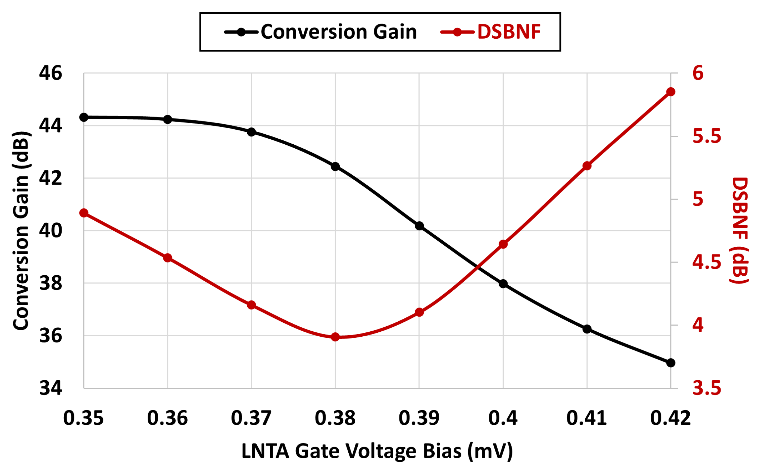
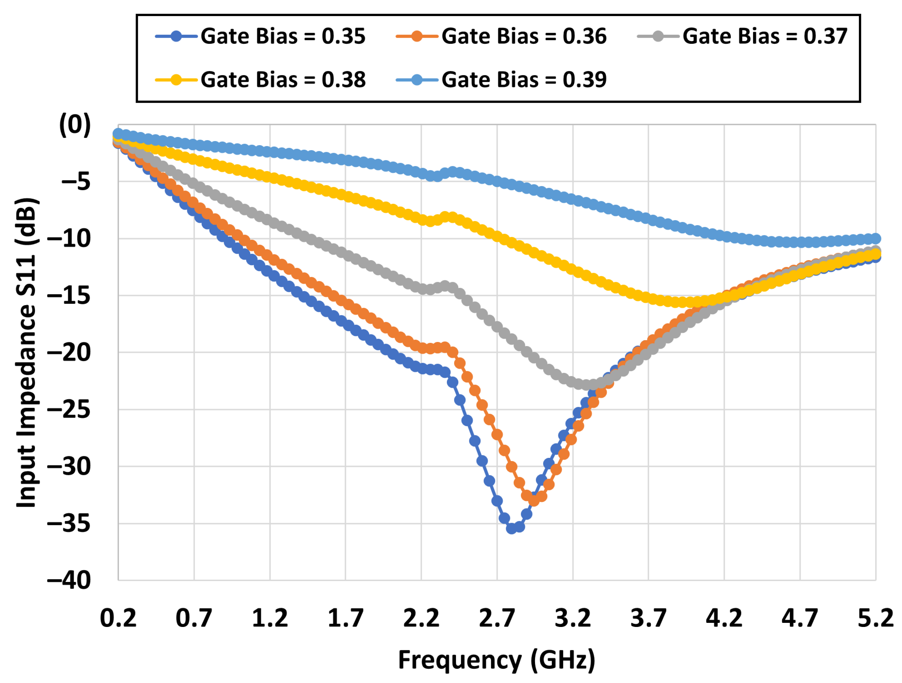
2.1. Low Noise Transconductance Amplifier
In CRR front-ends, the LNTA plays a significant role in defining the overall performance of the CRR, such as its sensitivity, input matching and power consumption. There are two well-known LNTA topologies that can be employed: common-source (CS) and common-gate (CG). The common-source topology is suitable for very low-noise applications, where the noise-figure (NF) is given by [13]
where is the transconductance, is the source impedance, is the channel effect, is the operating frequency, and is related to the maximum frequency at which that transistor can operate effectively (i.e., transition frequency). Equation (1) shows that a higher results in a very low NF in the CS LNTA topology. The NF in CG topology is given by
It is undeniable that the CG topology achieves much higher NF (>3 dB) than the CS topology since the second term in Equation (1) is suppressed by when . On the other hand, the CG topology is more suitable for wideband applications, while the CS topology results in narrow-band input impedance matching. The input impedance considering the CS LNTA is given by
where is a series gate inductor, is an source-degeneration inductor, is the gate to source capacitance, and is the parasitic capacitance considering the input of the LNTA, such as the pad and ESD cell capacitance. Equation (3) shows that the CS topology is suitable for narrow-band applications. On the other hand, the input impedance considering the CG LNTA is calculated by which is a real impedance. Hence, the CG LNTA topology is very suitable for wideband applications as it can be readily matched to the antenna (e.g., 50 ). Thus, topology selection for the LNTA depends on the application requirements. The receiver in [12] requires a wideband operation to cover a wide range of frequencies for several wireless standards; hence, the CG topology is suitable for this goal at the cost of a higher NF compared with the CS topology.
The LNTA design begins with an optimization of and . Figure 2a shows a test bench utilized to optimize and characterize and . Less than half of the supply voltage is applied to the drain terminal, which is close to the voltage that is expected after the receiver integration. The simulation is performed by sweeping the biasing current () while the width over length ratio (W/L) is maintained at constant value. To observe the channel-length effect, W and L are increased with a scaling coefficient from W/L to 5W/5L, resulting in the plots shown in Figure 2b,c. This shows that, by increasing the current for a given W/L, both and increase to a certain value until they flatten. The short channel effect can be reduced by increasing L. Thus, by increasing both W and L by the same scaling factor, improves. However, reduces due to the increase in gate-source and gate-drain capacitance. In the CG topology, is not the main contributor in the NF equation, but it is preferred to maintain it to be at least 10 times higher than the operating frequency to avoid any non-idealities such as oscillations. In this case, a scaling factor of 2 (i.e., 2W/2L) is selected. To achieve the required for input matching, both the width and the current need to increase. This can lead the circuit to consume high power. One approach to reduce the power consumption is to use the capacitive cross-coupling technique to boost the transconductance by a factor of 2. In this way, half of the current is required to achieve the required . The LNTA requires a current path to ground, and this can be achieved using either a resistor or inductor. In [12], an inductor is used to reduce the voltage headroom requirement and the RF signal loss by resonating with the parasitic capacitance. Note that further device optimization will need to be performed after receiver integration.
Figure 2.
(a) Test bench to optimize and characterize and , (b) resulting plots, and (c) resulting plots.
A single-ended antenna input needs to be converted to a differential signal at the input of the receiver. Both single to differential and LC baluns can be used. An LC-balun achieves a lower NF than a differential balun at the cost of a narrower bandwidth, but its combination with a CG LNTA topology provides wide bandwidth. Moreover, an LC-balun is able to convert the antenna impedance to any impedance considering the LNTA by adjusting the L and C values. This gives more flexibility to the design and allows it to operate at higher .
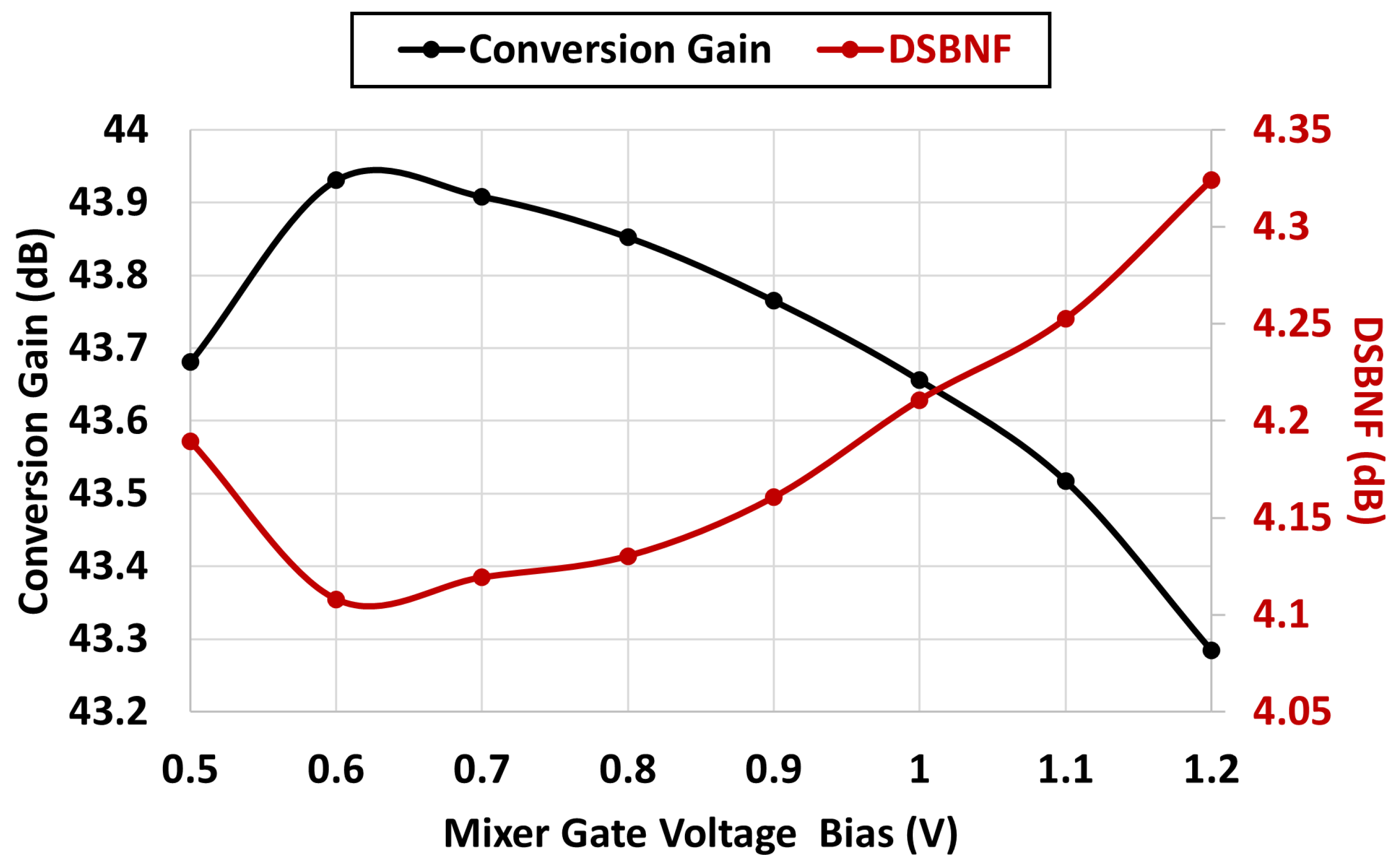
2.2. Down-Conversion Mixer
There are two choices of down-conversion mixers: active and passive. A passive mixer is preferred over an active mixer since active mixers require voltage headroom, which is not desirable due to the resulting poor linearity performance. Moreover, low-frequency noise can be filtered out using an AC-coupling capacitor at the input of the passive mixer. Thus, in [12], a passive mixer is used to down-convert the RF signal to the IF. A double-balanced passive mixer, as shown in Figure 1, is used. To design the mixer switches and optimize the W/L ratio, where L is minimum, a test bench that models the receiver front-end is employed as shown in Figure 3. In this test bench, the LNA and TIA are ideal macro-models. A voltage controlled current source (VCCS) is used to convert the RF voltage to the RF current to perform as an LNTA. The LNTA output impedance is modeled by R and C. , and an OpAmp model define the TIA macromodel. The design of the mixer switches is performed by sweeping the value of the W/L ratio and the gate voltage of the mixer switches concurrently in order to achieve the best NF and linearity. Figure 4 shows the NF and 1 dB compression point (P1dB) performance versus the W/L ratio and the gate voltage of the switches, VCM. The best integrated double side band noise figure (DSBNF), from 1 to 10 , is achieved at a VCM of 800 , while the P1dB at 600 is higher than at a VCM of 800 . Very large mixer switches need to be avoided to minimize large parasitic capacitors at the input of the mixer that attenuate the RF signal and cause LO to RF leakage. Thus, a W/L ratio of 35 / 130 is selected as a suitable trade-off value. Moreover, the gate voltage should be below the breakdown of the transistors when the LO signal switches high or low. Final optimization is needed after receiver integration.
Figure 3.
Test bench to design and optimize the down-conversion mixer switches.
Figure 4.
(a) The noise figure and (b) the 1 dB compression point versus the W/L ratio for different gate voltages of the input transistors.
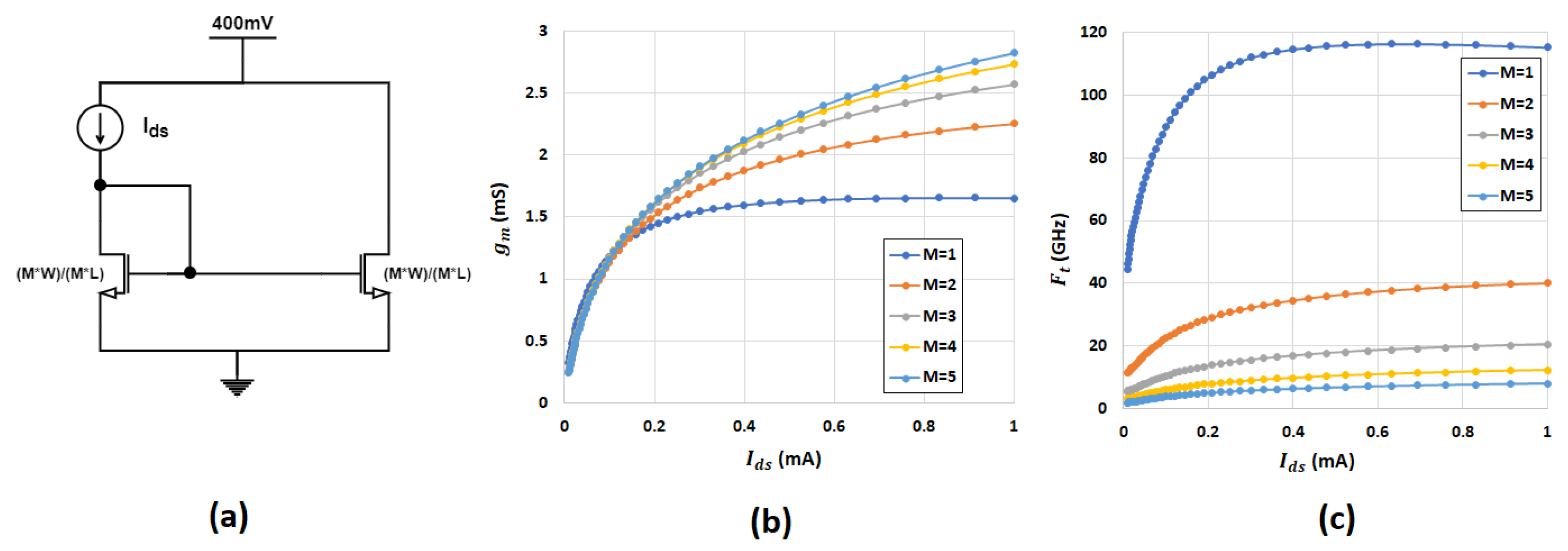
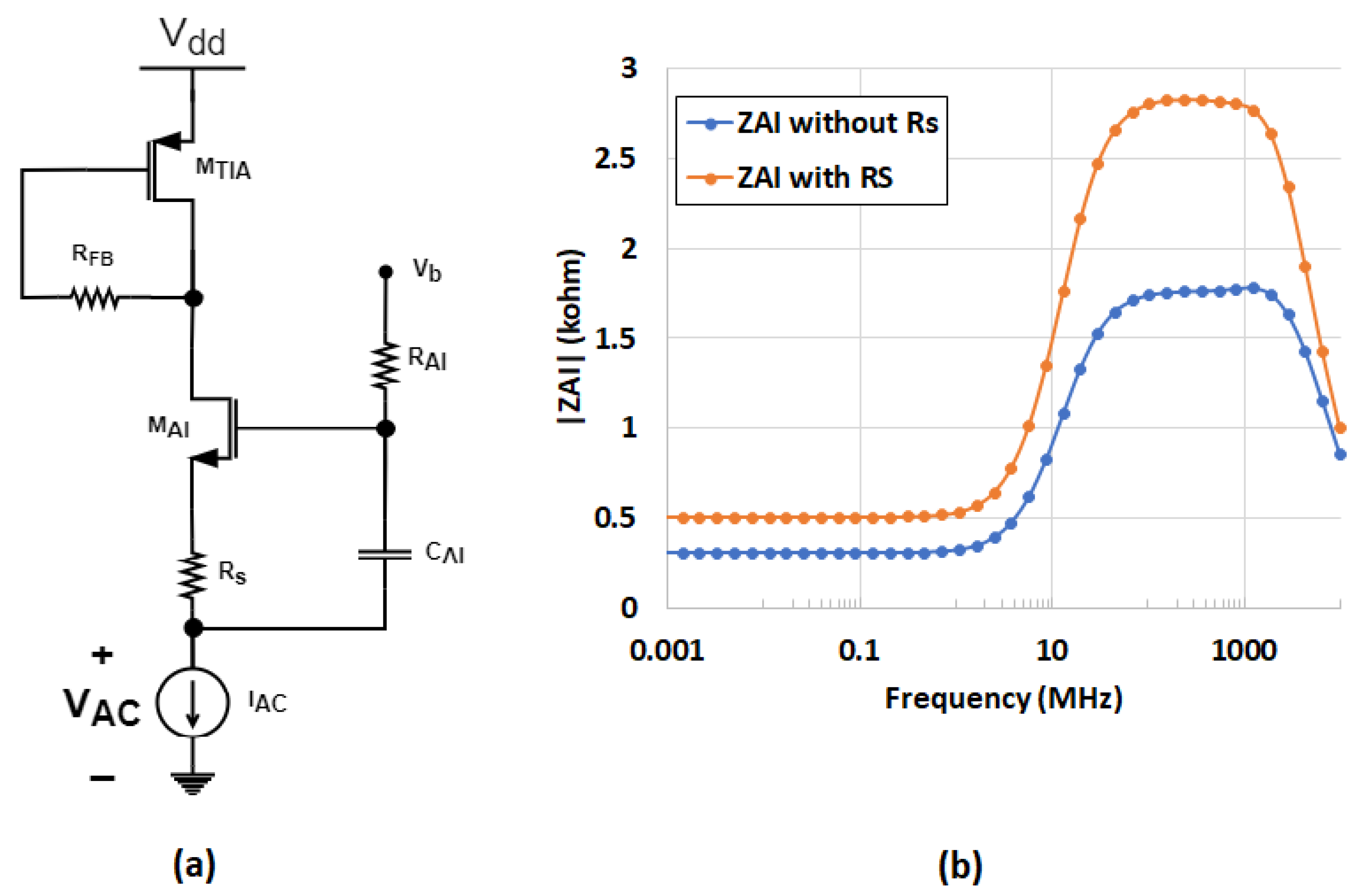
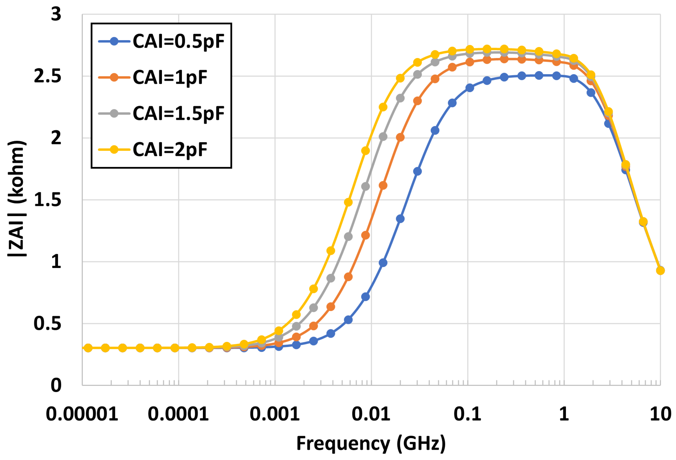
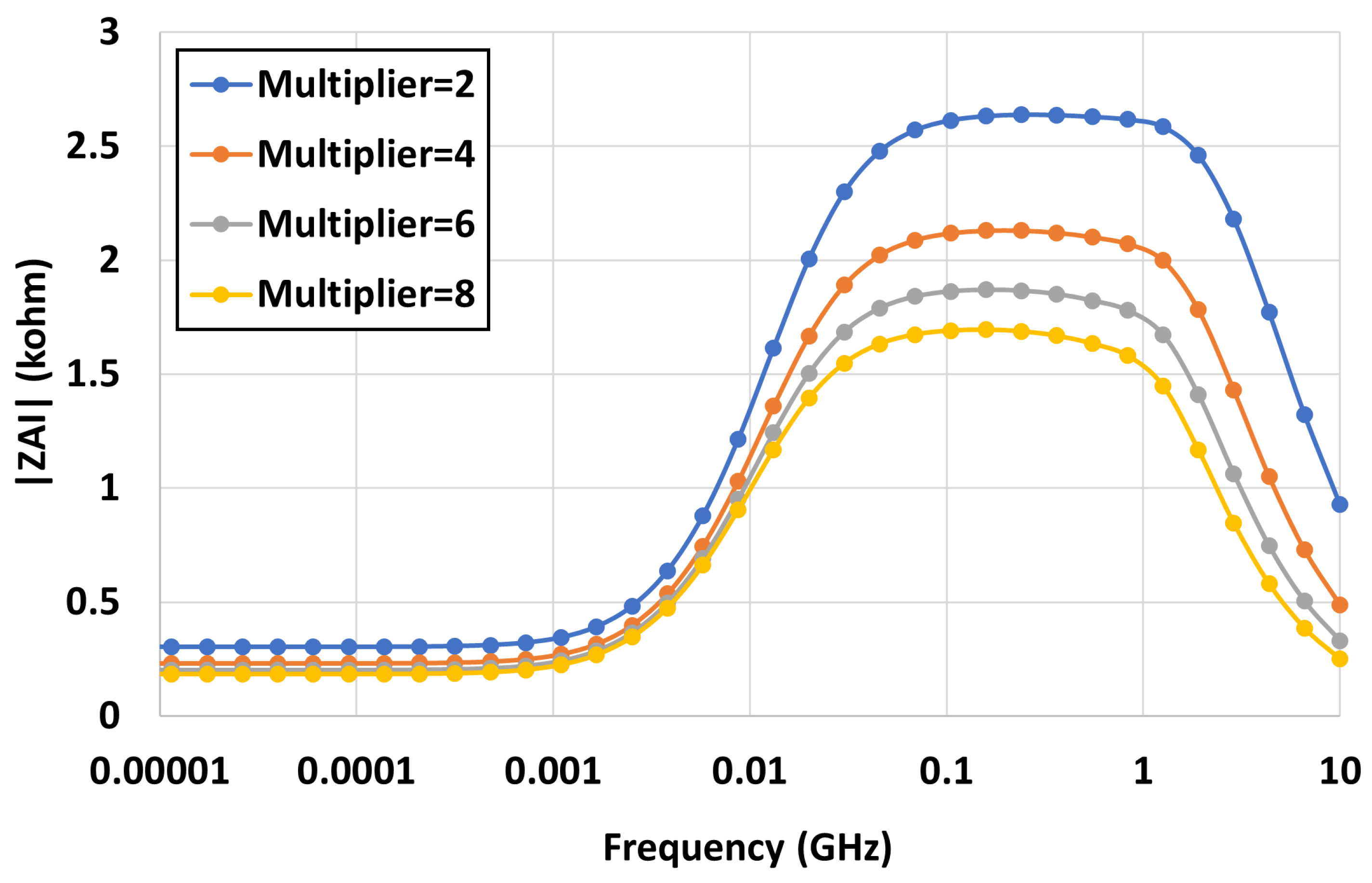
2.3. Active Inductor and Noise Cancellation
In [8], the mixer input and receiver output share the same node, which causes RF signal losses. As a result, the design is not able to operate at very high frequency and is more suitable to sub-GHz applications. In our earlier works [12], the concept of an AI was introduced. In this design, cascoded devices are used to boost the output impedance, as shown in Figure 1 (. The impedance considering the AI circuit, , by ignoring since it is in parallel, is summarized and given by
where is the parasitic capacitance at the mixer input and is related to the technology node.
The impedance from the LNTA to the AI is very small at lower frequencies and increases at higher frequencies. This helps to isolate the RF signal from the output node. In this case, the mixer input connects to the LNTA output directly, where the majority of the RF signal flows through the mixer input due to the lower input impedance compared to that of the AI.
Figure 5a shows the test bench to design the AI circuit. The AI circuit includes , and . is used to boost the impedance at higher frequencies. A small value is considered to avoid excessive voltage headroom usage. and are used to model the TIA circuit. and should be optimized to define the cut-off frequency. The transconductance of defines the impedance of the AI at DC and low frequencies. A small signal, , is applied to the input of the AI circuit, and is calculated to extract the input impedance of the AI circuit, . Figure 5b illustrates the magnitude of versus the frequency with and without being considered. It is obvious that helps to boost the AI input impedance at the cost of voltage headroom. Thus, there is a trade-off between the NF and linearity when the value of is defined. The gate terminal of needs to be biased with a voltage, , of 800 to keep it in saturation.
Figure 5.
(a) Test bench to design the active inductor and (b) its impedance magnitude over frequency with and without considered.
The magnitude of is shown for different values in Figure 6. This illustrates that a higher value pushes the cutoff frequency of to a lower frequency and increases its magnitude at high frequency, while it remains constant at lower frequencies. A value for of 1 shows a good trade-off value between the frequency cutoff and maximal impedance magnitude. Another step in the design of the AI circuit is to select the best W/L ratio of . Figure 7 shows that increasing the W/L ratio of with the multiplier from 2 to 8 leads to a higher and a lower magnitude at lower frequencies. A W/L ratio of M × 10 / 260 , where M is equal to 4, is selected as a good trade-off between low-frequency and high-frequency impedance behavior.
Figure 6.
Magnitude of for different values of .
Figure 7.
Magnitude of for different W/L ratio multipliers of transistor . The unit W/L ratio is 10 / 260.
Final component value fine tuning can be performed after receiver integration.
2.4. Transimpedance Amplifier
The final step is to design the baseband (BB) circuit in the CRR front-end where the BB current needs to be converted to a BB voltage at the output. In [8,12], a TIA is designed using a single transistor with a feedback resistor, , shown in Figure 1. A large channel-length value should be used to enhance the TIA output impedance. The impedance considering the TIA is defined by of . The conversion gain is approximately calculated through the following relation:
where is of transistor thanks to the capacitive cross-coupling technique, which boosts the by almost two times. should be large enough to achieve the required conversion gain. The output common-mode voltage can be slightly higher than half of the supply voltage in order to provide more voltage headroom for the AI and LNTA circuits. A value for of 1 is used to remove high-frequency components at the output of the mixer right before the TIA input.
After all of the aforementioned circuits are integrated within the CRR structure, an optimization needs to be performed by small adjustments to the component values in order to achieve the best possible performance.
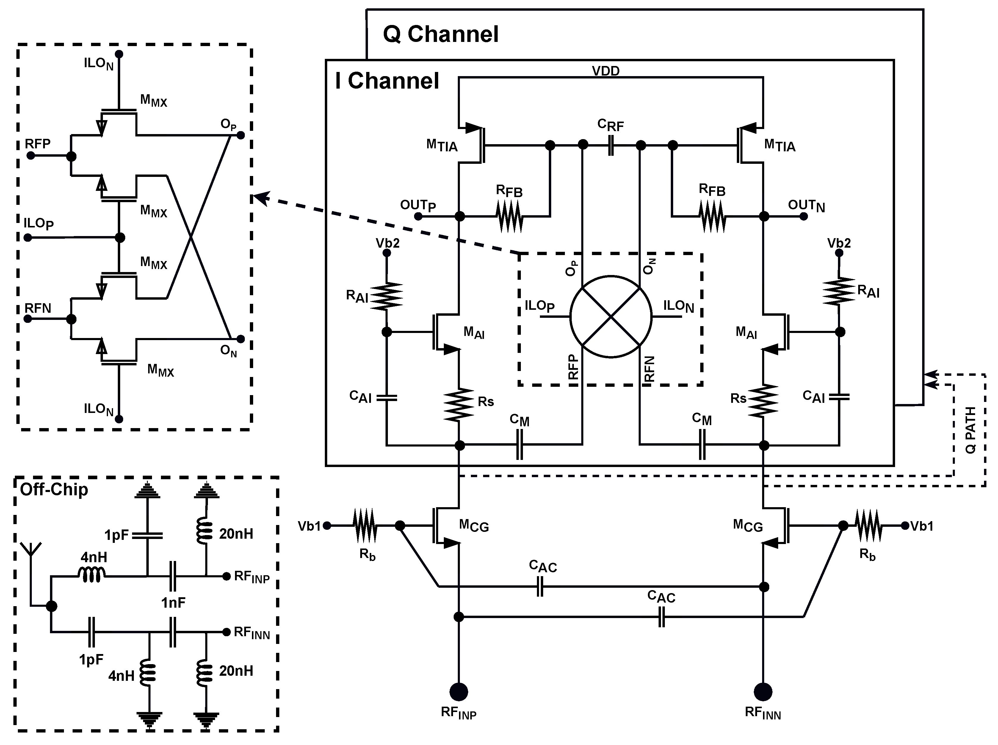
3. System Integration
CRR Front-End
The design of each circuit part of the CRR has been discussed in Section 2, which covered the design choices, theoretical analysis, design flow and test benches. The sub-blocks need to be integrated as shown in Figure 1 to form the CRR front-end. This includes the LNTA with external LC-balun to convert RF voltage to current, a passive mixer to convert the RF signal to a baseband current, a TIA to convert the baseband current to a voltage at the output and finally the AI circuit to isolate the RF signal from the output in order to reduce the RF signal loss.
The TIA, AI and LNTA are cascoded to share a single supply of . The performance of the CRR front-end should be verified through simulations versus several design metrics such as biasing voltages to make sure the design is robust. This begins with the NF and CG performance versus the gate voltage biasing of the LNTA, as shown in Figure 8. This illustrates that a voltage bias of 365–375 achieves almost a constant conversion gain and NF performance. The performance starts to degrade at higher biasing voltages due to the resulting poor input matching, as shown in Figure 9 and voltage headroom limitation. The starts degrading at biasing voltages above 380 since increases due to the larger device current stemming from the increase in .
Figure 8.
The NF and conversion gain versus the gate bias voltage of the LNTA.
Figure 9.
The input matching () versus frequency for several gate bias voltages of LNTA.
It is important to optimize the gate biasing voltage of the mixer switches. Figure 10 shows the NF and conversion gain of the CRR front-end versus the gate biasing of the mixer switches. It shows a flat conversion gain and NF performance versus a wide rage of biasing from to , which is beneficial to compensate for bias variations.
Figure 10.
The NF and conversion gain versus the gate bias voltage of the mixer.
The performance of the CRR front-end needs to be verified across a wide supply voltage range since the current-reuse architecture depends on the available voltage headroom. Figure 11 shows the NF and conversion gain performance versus the supply voltage sweep from 1 to . It shows a very stable performance versus the supply variations. The conversion gain changes by almost 3 from a supply going from to , and the NF is almost constant at .
Figure 11.
The NF and conversion gain versus supply variations.
Finally, the performance needs to be verified over the RF bandwidth from 1 to in order to cover the wideband operation of the studied receiver. Figure 12 shows the NF and CG performance versus the LO frequency. It shows that the conversion gain reduces while NF increases versus the LO frequency sweep due to the losses of the parasitic capacitors after the LNTA.
Figure 12.
The NF and conversion gain versus the LO frequency.
The linearity performance of the CRR front-end is verified through post-layout simulations in Section 5.
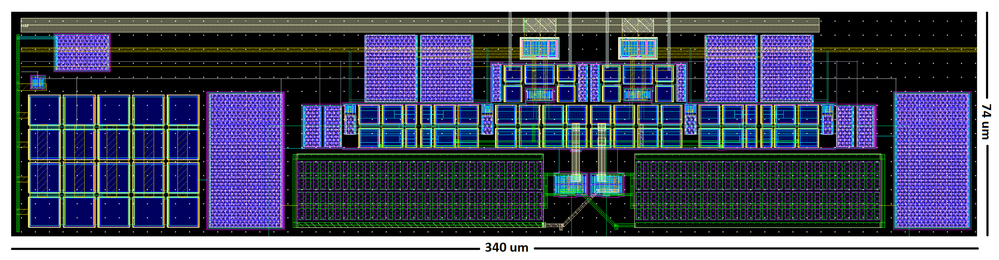
4. Layout Considerations
Analog circuit design is always challenging since many design metrics need to be considered while designing a circuit. This can be more complex when designing RF circuits. It is always crucial to think of the impact of the layout on the performance during the schematic level design. Thanks to the evolution of process design kits (PDKs), many layout non-idealities such as gate resistance and terminal-to-terminal capacitance are modeled in the RF device models. However, the routing effects and substrate leakage are not modeled at the schematic level. Hence, the layout considerations are discussed here in order to ensure the performance of the CRR front-end after post-layout simulations and ultimately after fabrication.
4.1. LNTA Layout
The LNTA is the first circuit in the receiver front-end that receives the weak signal. Routing to the LNTA input and output needs to have the minimum parasitic resistance to avoid the degradation of NF and and to ensure a minimum parasitic capacitance. In this case, top metal layers are preferred to reduce metal resistance and substrate leakage, but it is preferred to reserve the topmost metal layer for supply and ground routing. It is very important to keep routing resistance and capacitance low where the RF signal path passes through in areas such as the capacitive cross-coupling, which is used to enhance the transconductance. In the LNTA layout, it is beneficial to maintain the layout symmetry but avoid using any conventional analog matching techniques since these increase the parasitic capacitance. The capacitive loading effect on the inductor may change the resonant frequency. In this case, a capacitor of 1 should be added to the schematic during the schematic design phase, which can be reduced after post-layout simulation is performed. Vias always have high resistance; hence, it is preferred to increase the number of vias to reduce the resistance. This can worsen with the scaling down of the CMOS node.
4.2. Mixer Layout
The mixer layout is also important as it is paramount to maintain the symmetry in the mixer layout to avoid any non-idealities related to the even-order harmonics. It is also important to keep the parasitics at the gate and the source of the switches equal to avoid LO-RF and LO-IF feed-through. This can be done by carefully drawing the input, output and LO routes. While routing the LO path, it is essential to isolate it with ground routing underneath the LO routing to avoid the substrate leakage of the high-power LO signal that may degrade the performance of the entire chip. In this case, the LO signal can be routed with metal five while it is shielded by metal four, which is connected to ground. While designing the mixer, it should not be made very large to avoid parasitic loading on the RF ports.
4.3. Baseband Circuits
Layout considerations are more relaxed when it comes to the BB circuits. Nonetheless, the routing and circuits after the mixer should keep both symmetry and ensure matching, while parasitic capacitances are not as critical to minimize. While sizing the BB transistors, a sufficient number of fingers and multipliers needs to be used to match the components appropriately. Two well-known layout techniques can be used to perform the matching of baseband circuits: common-centroid and inter-digitization. In this work, inter-digitization is used to create the layout of the AI and TIA circuits. In BB circuits, parasitic resistance is important. Thus, low-resistance metal with sufficient width should be used.
4.4. Floor Plan
The complete integration of the sub-circuits requires routing from the pads to the LNTA input. The parasitic capacitance needs to be minimized as much as possible to reduce RF signal losses. It is essential to use high metal layers to draw routing to the LNTA input. Sensitive nets can use several pads to reduce the effect of wire bonding. It is suggested to employ high metal layers while connecting the sub-circuits as well. High metal layers can be used to connect the LNTA output to the mixer input, while lower metals can connect the BB and AI circuit. To avoid RF signal loss, the parasitic capacitance at the LNTA output needs to be reduced, as indicated in (6).
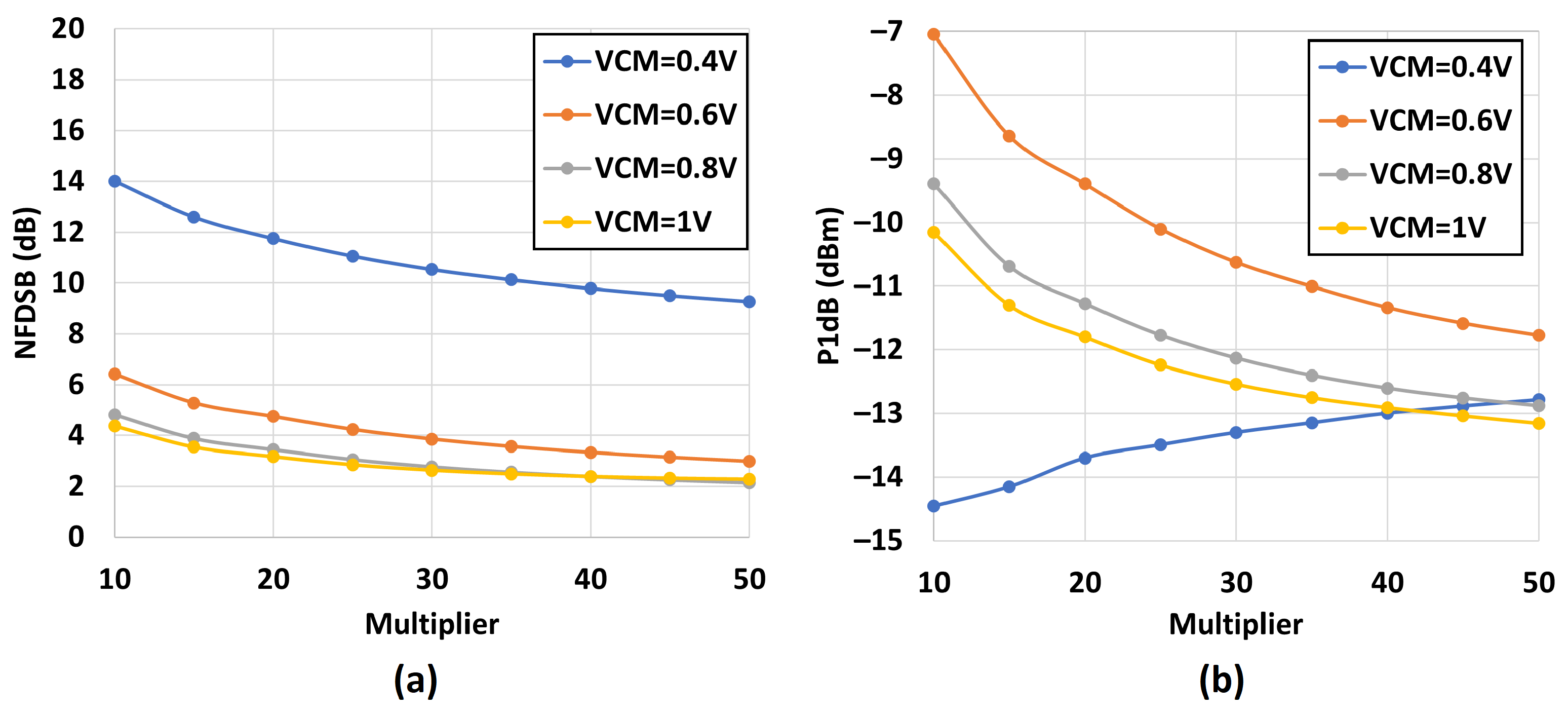
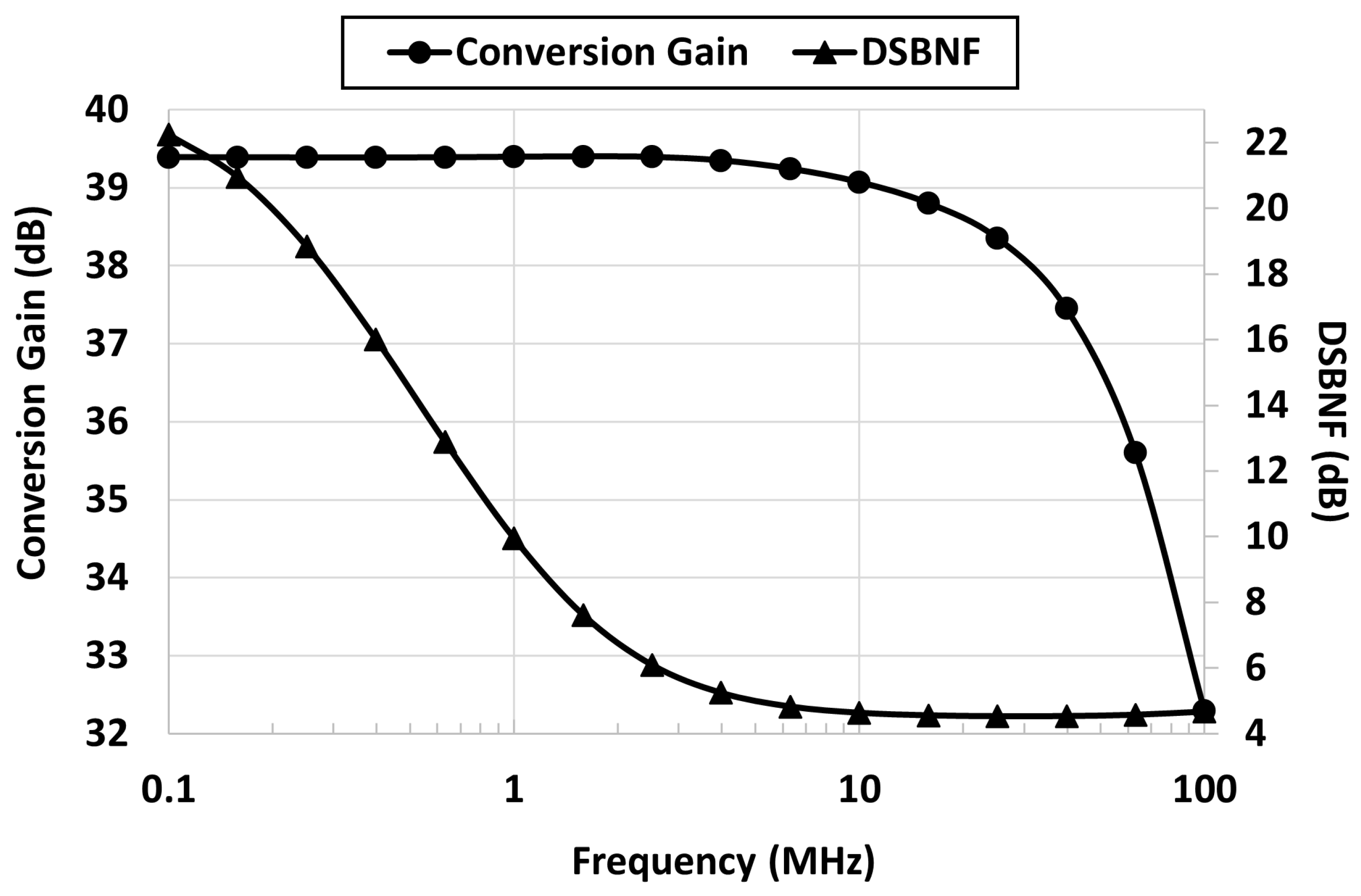
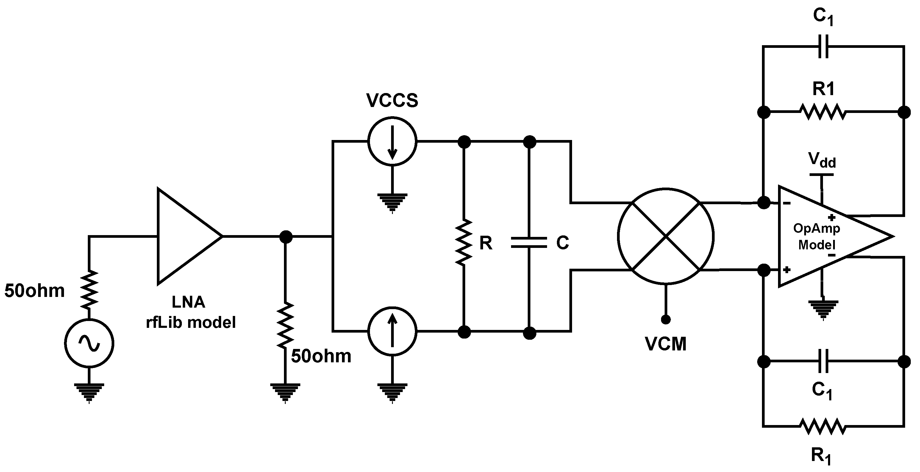
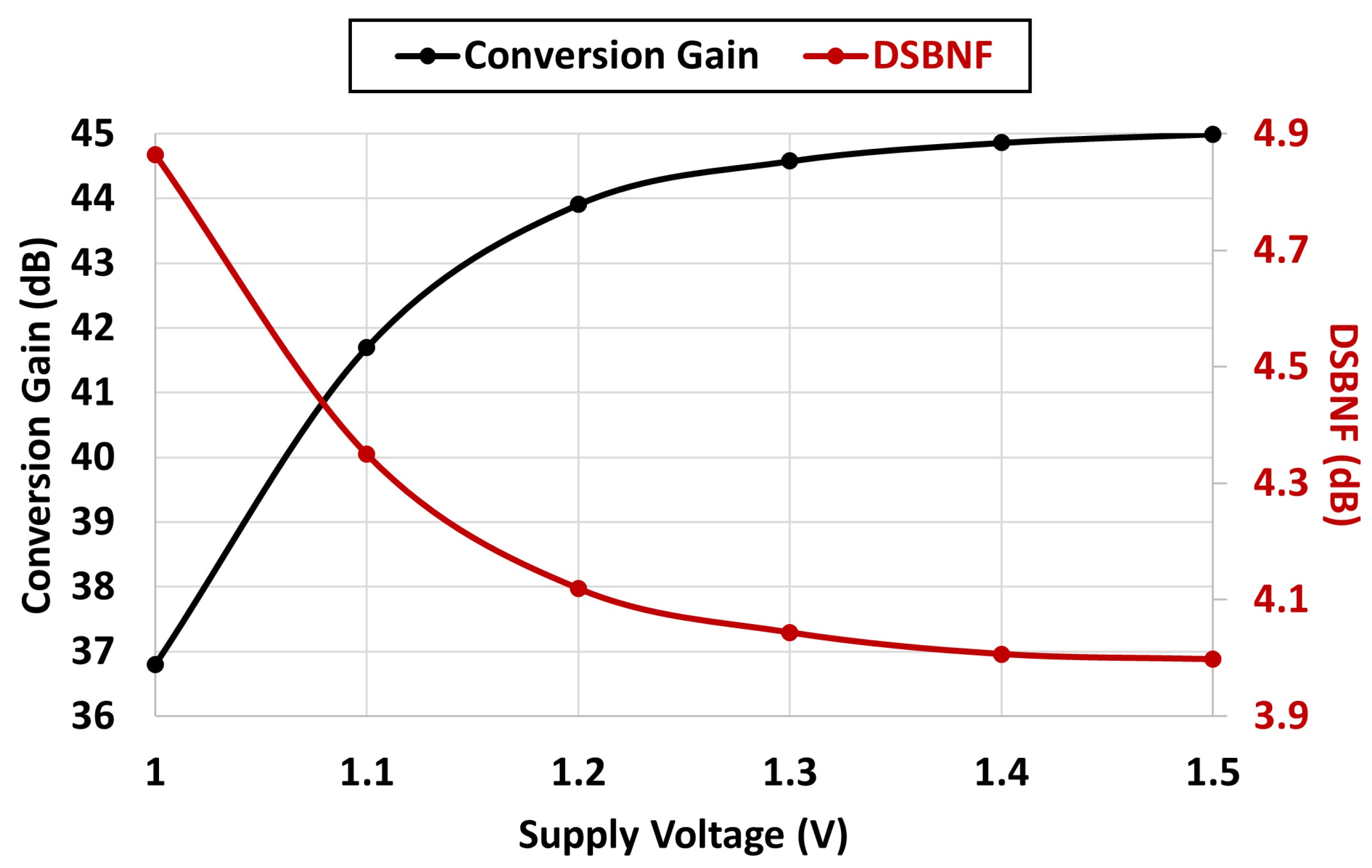
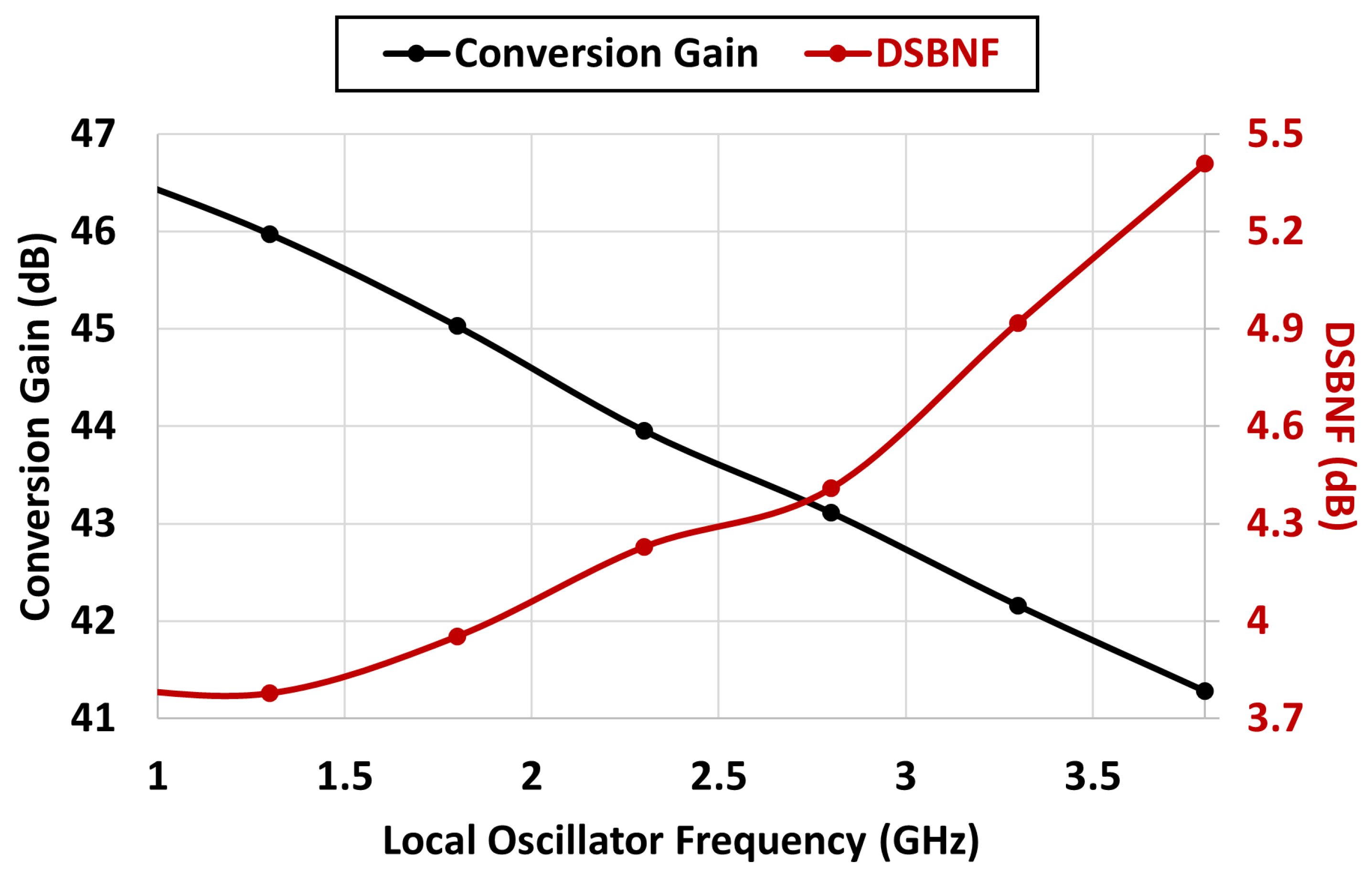
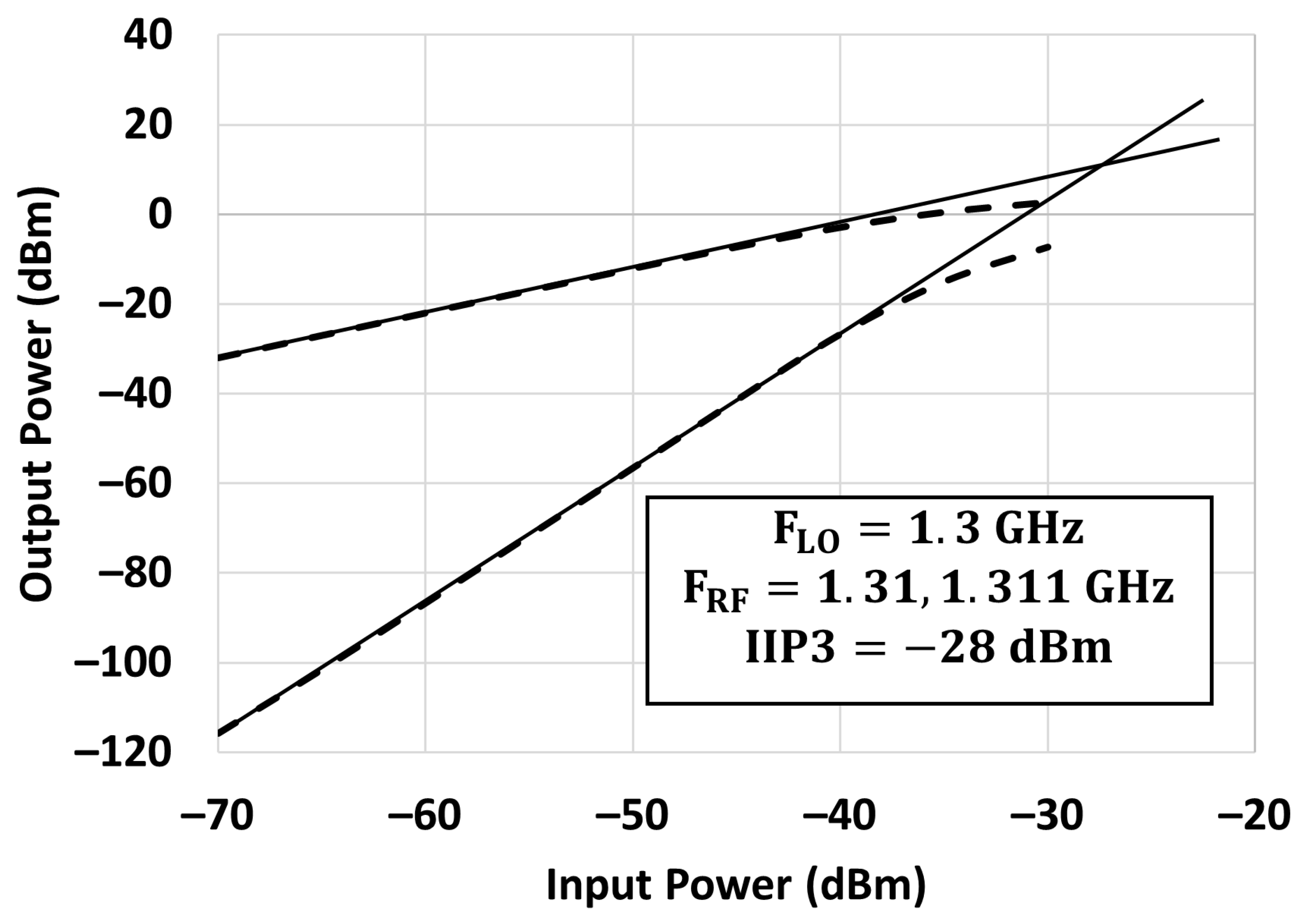
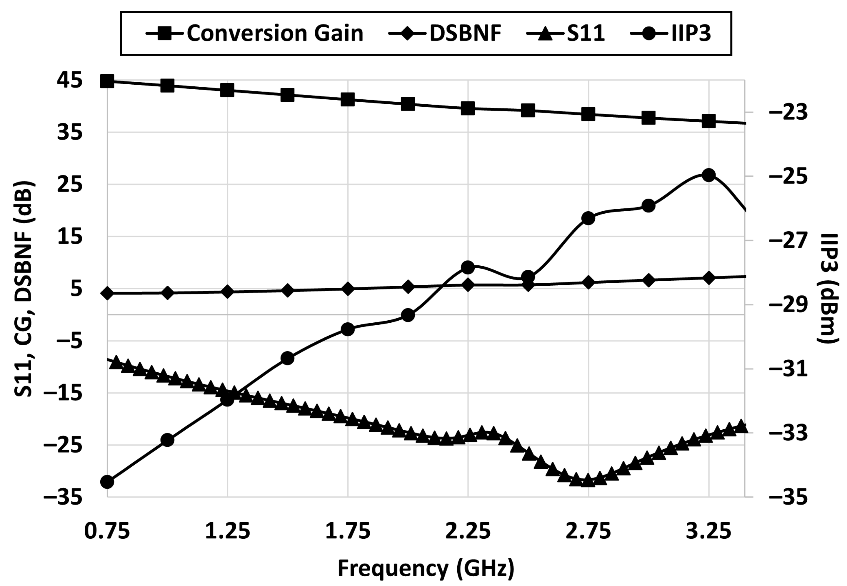
5. Post-Layout Simulation Results and Discussion
The wideband and low-power RF-to-baseband CRR front-end was implemented with TSMC 130 CMOS technology. The layout is shown in Figure 13. The CRR front-end only occupies an active area of 0.025 . It consumes a very low current of mA from a supply voltage of .
Figure 13.
The layout of CRR front-end. Reprinted with permission from Ref. [12]. Copyright 2022, Frederic Nabki.
The NF and conversion gain are post-layout simulated versus the IF, while the LO frequency is constant at , as shown in Figure 14. At frequencies above 10 , a flat NF of is achieved, while an integrated DSB NF of from to 20 is attained. A high low-frequency noise contribution comes from the direct coupling of the LNTA flicker noise to the baseband due to the low impedance path through the AI circuit at low frequencies. The receiver exhibits a conversion gain of over a wide IF 3dB-bandwidth of 40 . Although the conversion gain drops at high IF, the NF remains below 5 at up to 100 .
Figure 14.
The post-layout simulated NF versus the IF.
The linearity performance is verified by applying two tones of and at the input. This is performed while the LO frequency remains at . This generates fundamental tones of 10 and 11 and third-order intermodulation products of 9 and 12 at the output. The output power of the fundamental tone and third-order intermodulation products versus the input power are shown in Figure 15. An IIP3 of is achieved.
Figure 15.
The post-layout simulated fundamental and third-order intermodulation products versus the input power.
The receiver performance is verified with an RF input signal varying from to while the IF remains constant at 10 , as shown in Figure 16. The front-end exhibits an of less than over the entire RF range of interest. As the RF increases, the conversion gain reduces from to 36 , and the DSB NF increases from to . On the other hand, the IIP3 result improves from to due to the conversion gain reduction.
Figure 16.
Receiver post-layout simulated performance versus the RF signal.
The design’s capabilities and its overall performance are compared to prior works using the following figure of merit (FoM) used in [14] and given by
where and are the highest and lowest RF operating frequencies, respectively, F is the noise factor, IIP3 is the in-band IIP3 performance in , and is the power consumption. The results are shown in Figure 17, where the FoM for the proposed design and other references is plotted versus the power consumption. The FoM compares well considering the power consumption.
Figure 17.
Comparison of the FoM to prior works versus the power consumption. Tedeschi, M. 2010 [2]. Lin, Z. 2014 [4]. Lin, Z. 2014* [5]. Kim, S. 2019 [8]. Ramella, M. 2017 [11]. Park, B. 2021 [10].
Table 1 compares and summarizes the performance of the proposed receiver simulated here from the circuit proposed in [12] with the latest literature. This work compares well in terms of bandwidth and NF considering its technology node and power consumption.
Table 1.
Performance Summary and Comparison.
6. Conclusions
This work provided a design tutorial for the low-power and wideband RF-to-baseband CRR that was proposed in [12]. It discussed topology selection, design considerations and layout aspects for the LNTA, down-conversion mixer, AI circuit and TIA. The receiver is able to perform over the wide frequency band from 0.8 GHz to 3.4 GHz.
The proposed receiver in [12] was divided into four individual sub-circuits—LNTA, mixer, AI circuit and TIA—to be designed individually before integration. The design of each circuit was detailed through equations and simulations. Two well-known LNTA topologies, the CG and CS, were studied tomake sure that the best topology was selected to provide wideband performance. The AI circuit in [12] enhances the RF performance and addresses the issues raised in the literature. The TIA design used a single transistor, and design constraints and metrics were studied. Then, the test bench models to design and simulate each sub-circuit were also included. Finally, post-layout simulation results after the integration were presented, outlining the potential of the receiver and the viable design procedure described in this paper.
Author Contributions
Conceptualization, A.A. and F.N.; methodology, A.A.; software, A.A.; validation, A.A.; formal analysis, A.A.; investigation, A.A.; resources, A.A.; data curation, A.A.; writing—original draft preparation, A.A.; writing—review and editing, A.A. and F.N.; visualization, A.A.; supervision, A.A. and F.N.; project administration, A.A.; funding acquisition, F.N. All authors have read and agreed to the published version of the manuscript.
Funding
Received funding from NSERC (Natural Sciences and Engineering Research Council of Canada) for this research work.
Acknowledgments
The author would like to thank CMC Microsystems for chip fabrication and for providing the EDA tool.
Conflicts of Interest
The authors declare no conflict of interest.
Abbreviations
The following abbreviations are used in this manuscript:
| P1dB | 1 dB compression point |
| AI | Active inductor |
| BB | Baseband |
| CG | Common gate |
| CRR | Current-reuse receiver |
| CS | Common source |
| DUT | Design under test |
| DSB | Double side-band |
| ÉTS | École de technologie supérieure |
| FoM | Figure of merit |
| IF | Intermediate frequency |
| IoT | Internet of Things |
| LNTA | Low-noise transconductance amplifier |
| LO | Local oscillator |
| NF | Noise figure |
| DSBNF | Double side-band noise figure |
| PDK | Process design kit |
| RF | Radio frequency |
| TIA | Transimpedance amplifier |
| VCO | Voltage-controlled oscillator |
| VCCS | Voltage-controlled current source |
| VTH | Voltage threshold |
References
- Shams, N.; Abbasi, A.; Nabki, F. A 3.5 to 7 GHz Wideband Differential LNA with g m Enhancement for 5G Applications. In Proceedings of the 2020 18th IEEE International New Circuits and Systems Conference (NEWCAS), Montreal, QC, Canada, 16–19 June 2020; pp. 230–233. [Google Scholar]
- Tedeschi, M.; Liscidini, A.; Castello, R. Low-power quadrature receivers for ZigBee (IEEE 802.15. 4) applications. IEEE J. Solid-State Circuits 2010, 45, 1710–1719. [Google Scholar] [CrossRef]
- Cai, Z.; Shi, M.; Hu, S.; Wang, Z. A 2.4 GHz 2.9 mW Zigbee RF Receiver with Current-Reusing and Function-Reused Mixing Techniques. Electronics 2020, 9, 697. [Google Scholar] [CrossRef]
- Lin, Z.; Mak, P.I.; Martins, R.P. A 2.4 GHz ZigBee Receiver Exploiting an RF-to-BB-Current-Reuse Blixer+ Hybrid Filter Topology in 65 nm CMOS. IEEE J. Solid-State Circuits 2014, 49, 1333–1344. [Google Scholar] [CrossRef]
- Lin, Z.; Mak, P.I.; Martins, R.P. A Sub-GHz Multi-ISM-Band ZigBee Receiver Using Function-Reuse and Gain-Boosted N-Path Techniques for IoT Applications. IEEE J. Solid-State Circuits 2014, 49, 2990–3004. [Google Scholar] [CrossRef]
- Lin, F.; Mak, P.I.; Martins, R.P. An RF-to-BB-current-reuse wideband receiver with parallel N-path active/passive mixers and a single-MOS pole-zero LPF. IEEE J. Solid-State Circuits 2014, 49, 2547–2559. [Google Scholar] [CrossRef]
- Ghosh, D.; Gharpurey, R. A power-efficient receiver architecture employing bias-current-shared RF and baseband with merged supply voltage domains and 1/f noise reduction. IEEE J. Solid-State Circuits 2011, 47, 381–391. [Google Scholar] [CrossRef]
- Kim, S.; Kwon, K. A Low-Power RF-to-BB-Current-Reuse Receiver Employing Simultaneous Noise and Input Matching and 1/f Noise Reduction for IoT Applications. IEEE Microw. Wirel. Components Lett. 2019, 29, 614–616. [Google Scholar] [CrossRef]
- Abbasi, A.; Shams, N.; Kakhki, A.P.; Nabki, F. A low-power wideband receiver front-end for nb-iot applications. In Proceedings of the 2020 18th IEEE International New Circuits and Systems Conference (NEWCAS), Montreal, QC, Canada, 16–19 June 2020; pp. 50–53. [Google Scholar]
- Park, B.; Kwon, K. 2.4 GHz BLE Receiver With Power-Efficient Quadrature RF-to-Baseband-Current-Reuse Architecture for Low-Power IoT Applications. IEEE Access 2021, 9, 62734–62744. [Google Scholar] [CrossRef]
- Ramella, M.; Fabiano, I.; Manstretta, D.; Castello, R. A SAW-less 2.4-GHz receiver front-end with 2.4-mA battery current for SoC coexistence. IEEE J. Solid-State Circuits 2017, 52, 2292–2305. [Google Scholar] [CrossRef]
- Abbasi, A.; Shams, N.; Nabki, F. A 0.8–3.4 GHz, low-power and low-noise RF-to-BB-Current-Reuse receiver front-end for wideband local and wide-area IoT applications. In Proceedings of the 2020 27th IEEE International Conference on Electronics, Circuits and Systems (ICECS), Glasgow, UK, 23–25 November 2020; pp. 1–4. [Google Scholar]
- Razavi, B. RF Microelectronics: Pearson New International Edition; Pearson Education Limited: London, UK, 2013. [Google Scholar]
- Bozorg, A.; Staszewski, R.B. A 0.02–4.5-GHz LN (T) A in 28-nm CMOS for 5G exploiting noise reduction and current reuse. IEEE J. Solid-State Circuits 2020, 56, 404–415. [Google Scholar] [CrossRef]
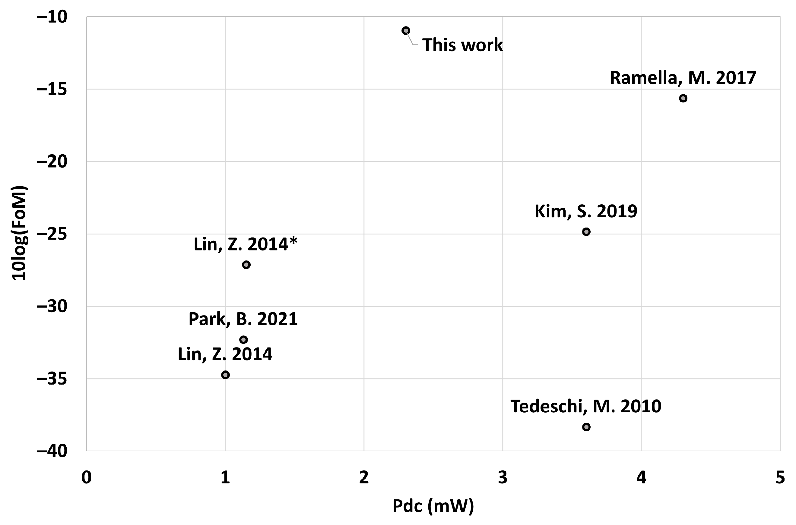
Publisher’s Note: MDPI stays neutral with regard to jurisdictional claims in published maps and institutional affiliations. |
© 2022 by the authors. Licensee MDPI, Basel, Switzerland. This article is an open access article distributed under the terms and conditions of the Creative Commons Attribution (CC BY) license (https://creativecommons.org/licenses/by/4.0/).