Article

Analysis and Design of an S/PS−Compensated WPT System with Constant Current and Constant Voltage Charging

1
College of Electronic and Electrical Engineering, Henan Normal University, Xinxiang 453007, China
2
College of International Education, Henan Normal University, Xinxiang 453007, China
3
Henan Key Laboratory of Optoelectronic Sensing Integrated Application, Henan Normal University, Xinxiang 453007, China
4
Academician Workstation of Electromagnetic Wave Engineering of Henan Province, Henan Normal University, Xinxiang 453007, China
*
Author to whom correspondence should be addressed.
Electronics 2022, 11(9), 1488; https://doi.org/10.3390/electronics11091488
Submission received: 27 March 2022 / Revised: 27 April 2022 / Accepted: 2 May 2022 / Published: 6 May 2022

Abstract

:
In recent years, more and more scholars have paid attention to the research of wireless power transfer (WPT) technology, and have achieved a lot of results. In practical charging application, ensuring that the WPT system can achieve constant current and constant voltage output with zero phase angle (ZPA) operation is very important to prolong battery life and improve power transfer efficiency. This paper proposes an series/parallel series(S/PS)-compensated WPT system that can charge the battery load in constant current and constant voltage modes at two different frequency points through frequency switching. The proposed S/PS structure contains only three compensation capacitors, few compensation elements, simple structure, low economic cost, in addition, the secondary-side does not contain compensation inductor, ensuring the compactness of the secondary-side. An experimental prototype with an input voltage of 40 V is established, and the experiment proves that the model can obtain output voltage of 48 V and current of 2 A. Maximum system transmission efficiency of up to 92.48% The experimental results are consistent with the theoretical analysis results, which verifies the feasibility of the method.

1. Introduction

Wireless power transfer (WPT) technology is a rapidly developing contactless power supply technology. WPT technology is mainly divided into magnetic field coupling, electric field coupling and electromagnetic radiation type according to the different energy transmission media. The main method used in this paper is magnetic coupling. Compared with the traditional plug-in charging, WPT technology has the advantages of being safer, more efficient, flexible and convenient [1,2]. Therefore, WPT technology has been widely used in electric vehicle charging [3,4,5], implantable medical devices [6,7], underwater power [8,9], convenient consumer electronics [10,11] and other industrial fields [12,13,14].
Nowadays, high-performance lithium-ion batteries are widely used in real life with the advantages of high efficiency and high-power density. Figure 1 shows the variation pattern of each parameter in a typical battery charging [15]. The battery charging process is mainly divided into two charging modes, stage I and stage II. Stage I represents the constant current (CC) charging mode and stage II represents the constant voltage (CV) charging mode. The charging is initially located in stage I, the charging current firstly remains constant and the charging voltage rises. When the charging voltage reaches the preset voltage, the charging mode switches from stage I to stage II. Then, the charging voltage remains constant and the charging current gradually starts to decrease exponentially, when the charging current drops to a specific value, the whole charging process ends. The equivalent resistance of the battery gradually increases throughout the charging process. To prolong the life of the battery, it needs to be charged sequentially in constant current and constant voltage mode. In addition, it is crucial for the WPT system to work in ZPA operation to improve the transfer efficiency and avoid reactive power loss.
The study of control strategies and compensation topologies are the main approaches to achieve CC or CV output for WPT technology. However, achieving CC or CV output by means of control tends to increase the complexity of WPT system design. To simplify the design, many scholars have chosen to innovate on the traditional four basic topologies of series/series (S/S), series/parallel (S/P), parallel/series (P/S), and parallel/parallel (P/P) [16,17]. In order to meet the battery charging requirements, the hybrid structure with the combination of two traditional topologies is proposed in the actual circuit design. For example, a hybrid topology with S-S and S-P working in cooperation or S-P and P-P working in cooperation is proposed to achieve stable CC and CV charging characteristics [18,19]. Refs. [20,21,22,23] proposed adding AC switches to the topology circuit, and the topology of the system is changed by acting the switch during the charging process, so as to achieve the switching between CC and CV outputs. However, the disadvantage is that additional AC switches and corresponding driving circuits are required in the system, which undoubtedly increases the complexity and cost. Based on the above problems, ref. [24] proposed a new approach to switch between CC and CV modes by switching the operating frequency. However, it uses SS topology structure, which suffers from the problem that the ZPA cannot be satisfied in CV mode and will lead to a huge power loss. On the basis of [24], ref. [25] reasoned and verified that the dual LCC WPT system is able to satisfy ZPA operation in both CC and CV modes. Refs. [26,27,28] both used a similar approach and proved that the proposed WPT system can achieve CC and CV outputs at two different frequency points, respectively. Then, CC and CV charging of the battery is achieved by controlling the mode selection switch. Nevertheless, they face the problem of indispensable compensation inductor or coil as well as excessive total number of compensation components in the structure. In general, the weight, size and cost characteristics of the compensation inductor are generally higher than those of the compensation capacitor for the same volt-ampere rating conditions. In addition, the internal resistance of compensation inductor is also usually larger than compensation capacitor. Hence, the topologies mentioned in [25,26,27,28] all suffer from relatively high cost, bulk, and loss.
Based on the above stated problems, this paper proposes an series/parallel series(S/PS)−compensated WPT system which can achieve CC and CV outputs at two different ZPA frequencies. The compensation elements of the proposed S/PS−topology contain only three capacitors, which not only allows the system to avoid the use of compensation inductors or redundant coils, but also reduces the total number of compensation components in the system.
This paper is composed of six sections. In the second section, a comprehensive theoretical analysis of the proposed S/PS−compensated WPT system is provides, and the condition equations satisfying CC and CV outputs as well as ZPA operation are derived. In the third section, based on the second section, the design method of the system compensation elements is introduced in detail and the proposed theory is initially verified by simulation. In the fourth section, the CC/CV mode selection switch is introduced and its working principle is analyzed. In the fifth section, an experimental prototype is fabricated and the feasibility of the theoretical analysis is further verified through experiments. The last section is the conclusion of this paper.

2. Theoretical Analysis of the S/PS−Compensated WPT System

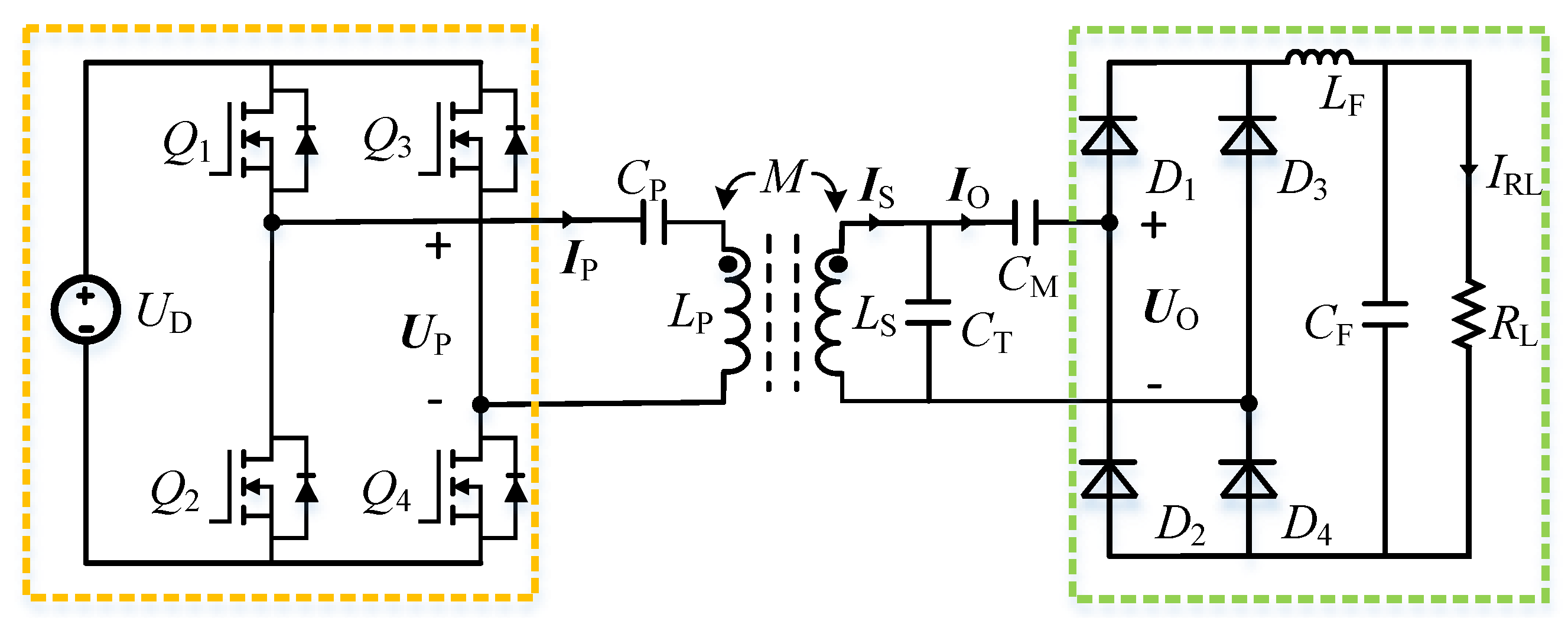
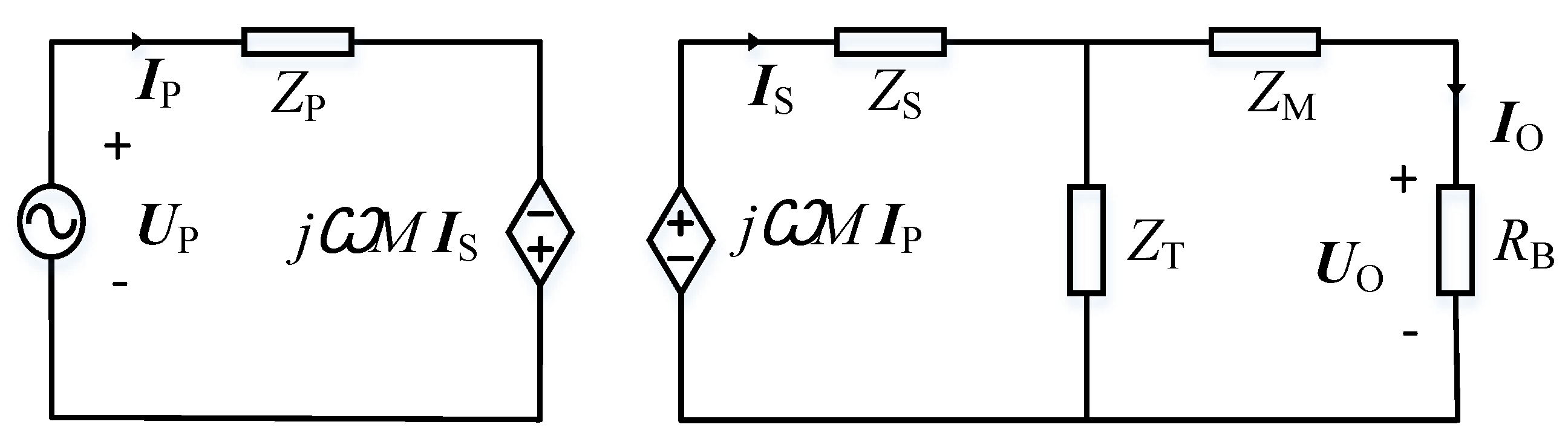
2.1. Overview of the S/PS-Compensated WPT System

The proposed S/PS−compensated WPT system is depicted in Figure 2. UD is a constant DC input voltage source for power the high-frequency inverter (HFI). The HFI is constituted by four MOSFETs (Q1Q4) and output voltage is UP, which is used to drive the primary-side coil. The HFI operating frequency is denoted by f, while the operating angular frequency is denoted ω (ω = 2πf). LP and LS are self-inductances of the primary-side coil and secondary-side coil, respectively, RP and RS are the corresponding parasitic resistances, respectively. M stands for the mutual inductance between the primary-side coil and secondary-side coil. CP is the primary-side compensation capacitor connected in series with LP. CT and CM are the secondary-side series and parallel compensation capacitors, respectively. The full−bridge uncontrolled rectifier with input voltage UO which is composed of four Schottky diodes (D1D4) is connected to the battery load through the filter circuit consisting of LF and CF.
Figure 3 shows the equivalent circuit diagram of the S/PS−compensated WPT system. UP is the root−mean−square (RMS) value of the square wave voltage source generated by the HFI. The expression of UP is given as:
U P = 2 2 π 2 U D
RB is the equivalent AC load resistance of the part circled by the green dashed line in Figure 2. According to [25], RB can be calculated by:
R B = 8 R L π 2
For simplify, the parasitic resistances of coils and the compensation capacitors in the circuit are ignored in this paper. ZP, ZS, ZT and ZM are the corresponding equivalent impedances, which can be defined as follow.
Z P = j ω L P + 1 j ω C P Z S = j ω L S Z T = 1 j ω C T Z M = 1 j ω C M
According to Kirchhoff’s voltage law (KVL), the mathematical equation of the equivalent circuit in Figure 3 can be obtained as:
U P = Z P I P j ω M I S 0 = j ω M I S + Z S I S + Z T ( I S I O ) 0 = Z T ( I S I O ) + ( Z M R B ) I O
where IP, IS and IO represent the current flowing through LP, LS and CM, respectively. Based on (3), the corresponding current phasors can be solved as:
I P = Z M Z T + Z T Z S + Z S Z M + ( Z S + Z T ) R B A + B R B U P I O = j ω M Z T A + B R B U P
To simplify the denominator in the resulting current phasor expression, the letters A and B are respectively defined as:
A = Z P Z M Z S + Z P Z M Z T + Z P Z S Z T + ω 2 M 2 Z T + ω 2 M 2 Z M B = Z P Z S + Z P Z T + ω 2 M 2

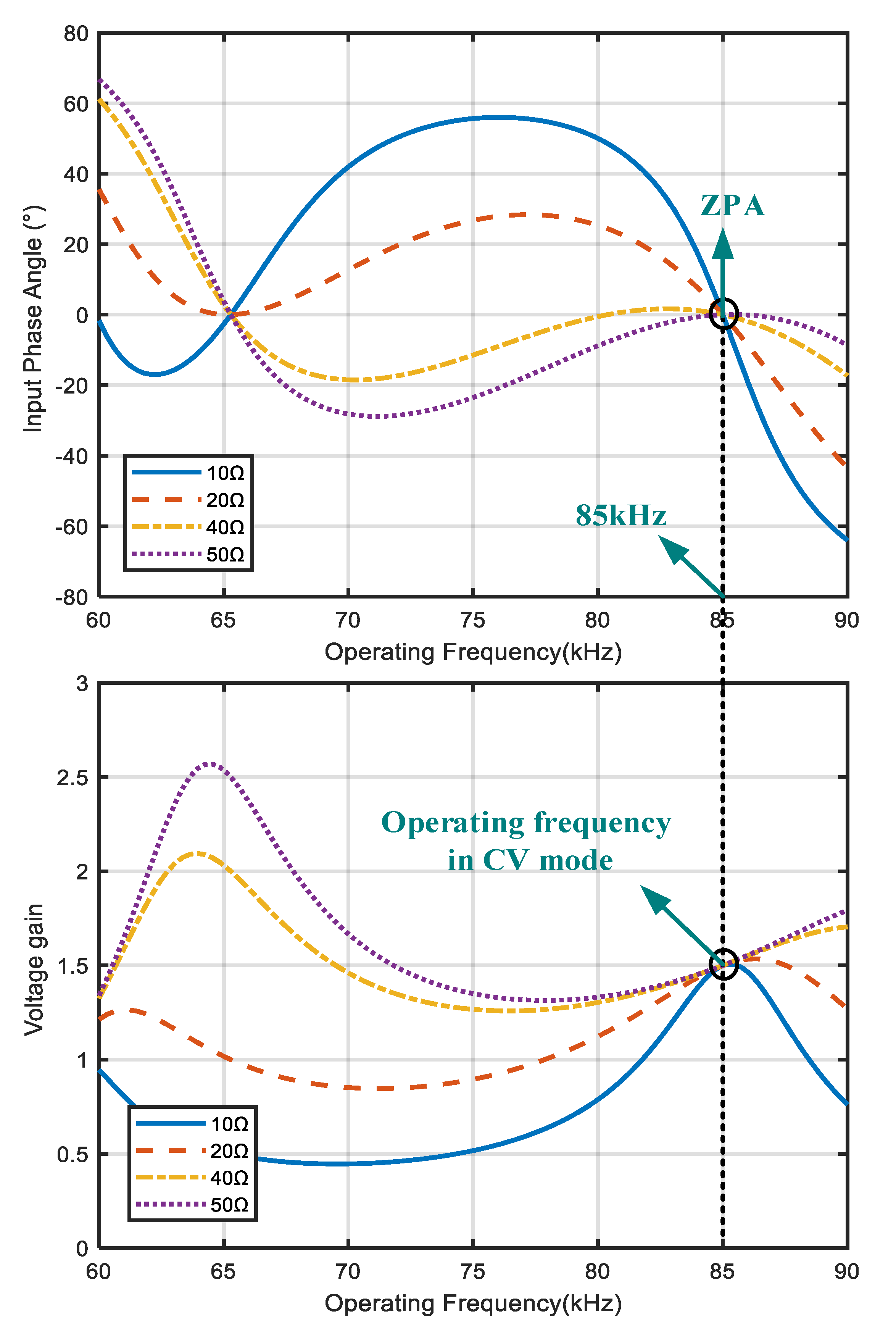
2.2. Analysis of the CV Characteristic with ZPA Operation

Based on Equation (5), the mathematical expression of the voltage gain E(ωcv) = UO/UP and the input impedance Zin = UP/IP can be derived as:
E ( ω c v ) = U O U P = j ω C V M Z T R B A + B R B
Z i n ( ω C V ) = U P I P = A + B R B Z M Z T + Z T Z S + Z S Z M + ( Z S + Z T ) R B
By observing Equation (7), to enable the proposed S/PS−compensated WPT system to achieve the output voltage that does not vary with the load, the mathematical expression of the voltage gain E(ωcv) should not contain RB. It is easily obtained that RB can be approximately dropped when A = 0, and then the proposed S/PS−compensated WPT system can achieve load−independent CV output. Then, the following equation can be obtained.
A = Z P Z M Z S + Z P Z M Z T + Z P Z S Z T + ω C V 2 M 2 Z T + ω C V 2 M 2 Z M = 0
Meanwhile, it is also crucial to meet ZPA operation for improving system energy transfer efficiency and avoiding reactive power loss. Thus, substituting Equation (9) into Equation (8), the input impedance Zin(ωcv) can be further derived as:
Z i n ( ω C V ) = B R B Z M Z T + Z T Z S + Z S Z M + ( Z S + Z T ) R B
It can be seen from (10) that when Equation (11) holds, the input impedance of the system is purely resistive.
Z S + Z T = 0
Then, substituting Equations (9) and (11) into Equations (7) and (10), the voltage gain E(ωcv) and the input impedance Zin can be further simplified as:
E ( ω C V ) = Z S + Z T = 0 A = 0 = j Z T ω C V M
Z in ( ω C V ) = Z S + Z T = 0 A = 0 = ω C V 2 M 2 R B Z T Z S
As evident from Equations (12) and (13), when Equations (9) and (11) hold, the voltage gain E(ωcv) and the input impedance Zin(ωcv) of the proposed S/PS−compensated WPT system are not affected by changes in load. In other words, if the parameters of the system are designed reasonably, the proposed S/PS−compensated WPT system can obtain the load−independent constant voltage output, and the system can always operate under the ZPA condition.

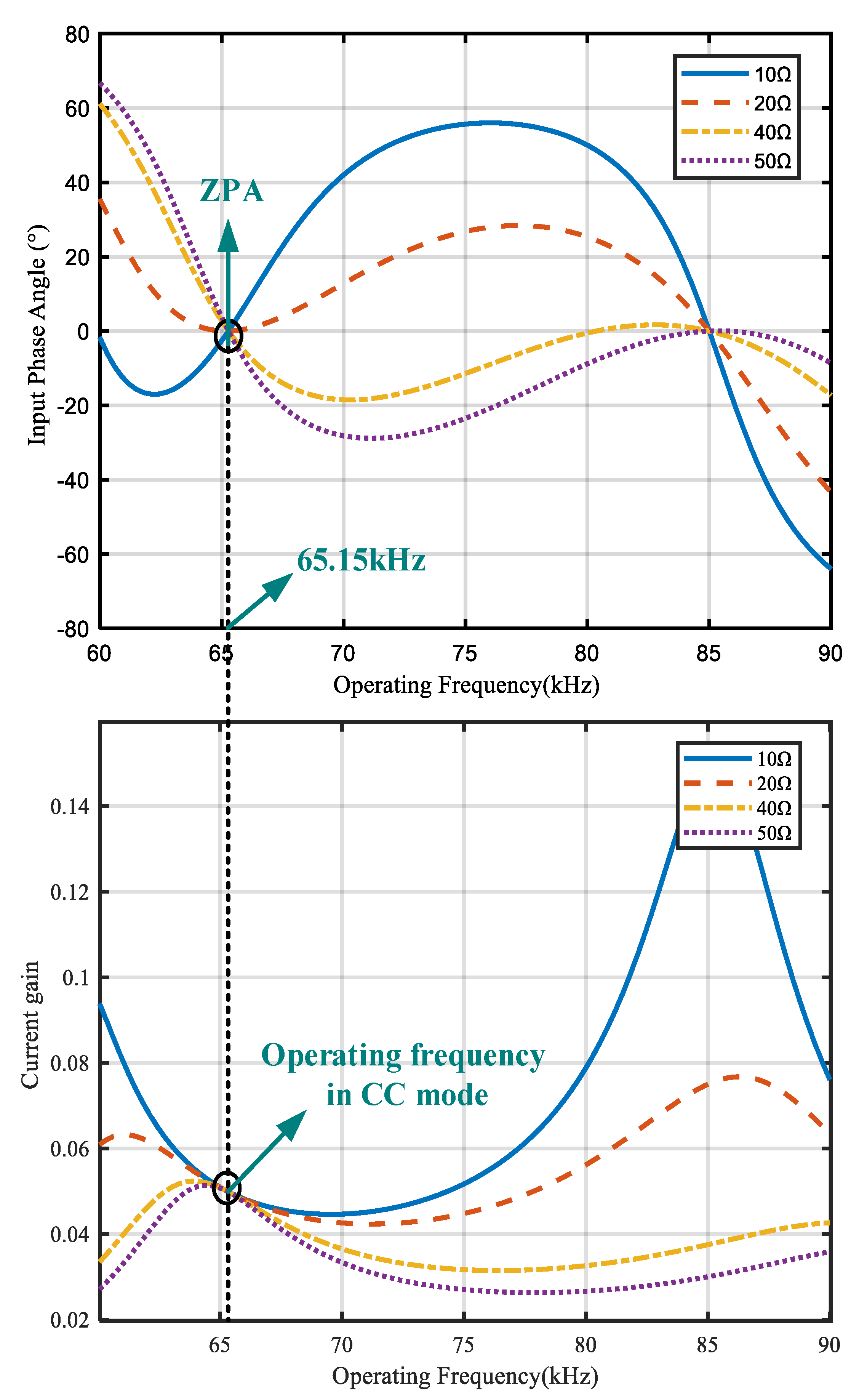
2.3. Analysis of the CC Characteristic with ZPA Operation

The analysis process of CC is consistent with the basic idea of the overall analysis summarized in the previous section. First, the transconductance gain G(ωcc) = IO/UP is defined. The topologies in CC and CV modes are the same, but the difference is the operating frequency. The angular frequency for CC mode is set to ωcc. Therefore, according to Equation (5), the transconductance gain G(ωcc) is calculated as:
G ( ω C C ) = I O U P = j ω C C M Z T A + B R B
When it is required to realize the CC output characteristic, it is necessary to make the expression of the transconductance gain G(ωcc) in Equation (14) exclude RB. By observing Equation (14), the above analysis result can be realized when Equation (15) is satisfied.
B = Z P Z S + Z P Z T + ω C C 2 M 2 = 0
In the same way, it can be obtained that the input impedance of the system in the CC mode is the same as the equation in the CV mode, only the operating frequency is different, as shown in Equation (16).
Z i n ( ω C C ) = U P I P = A Z M Z T + Z T Z S + Z S Z M + ( Z S + Z T ) R B
Observing Equation (16), it can be seen that when Equation (17) holds, the input impedance Zin(ωcc) of the system in the CC mode is purely resistive and the ZPA operation can be realized.
Z M Z T + Z T Z S + Z S Z M = 0
Substituting Equations (15) and (17) into Equations (14) and (16), the simplified form of the transconductance gain G(ωcc) and the input impedance Zin(ωcc) are obtained as shown in (18) and (19), respectively.
G ( ω C C ) = Z M Z T + Z T Z S + Z S Z M = 0 B = 0 = j Z T ω C C M ( Z T + Z M )
Z i n ( ω C C ) = Z M Z T + Z T Z S + Z S Z M = 0 B = 0 = ω C C 2 M 2 ( Z T + Z M ) ( Z T + Z S ) R B
As evident from Equations (18) and (19), when Equations (15) and (17) hold, the transconductance gain G(ωcc) and the input impedance Zin(ωcc) of the proposed S/PS−compensated WPT system are not affected by changes in load. In other words, if the parameters of the system are designed reasonably, the proposed S/PS−compensated WPT system can obtain the load−independent constant current output, and the system can always operate under the ZPA condition.

2.4. Expression of Compensation Capacitor

In Section 2.2, it is analytically known that the proposed S/PS−compensated WPT system can achieve CV charging output and ZPA operation when Equations (9) and (11) hold together under the condition of CV angular frequency ωcv. In Section 2.3, it is proved by theoretical analysis that the proposed S/PS−compensated WPT system can achieve CC charging output and ZPA operation when Equations (15) and (17) hold together under the condition of CC angular frequency ωcc. Therefore, in order to achieve the CC and CV outputs respectively at two different ZPA frequency points, the set of compensation elements must simultaneously satisfy the five Equations (9), (11), (15), (17) and (18). By associating the five equations, the expressions for the three compensation capacitors can be solved as in (20). The definition of C in (20) is shown in (21).
C T = 1 ω C V 2 L S C P = 4 M G 2 ( ω C C ) ( ω C V 2 C 2 ω C V 4 4 ) ( 2 M 2 G ( ω C C ) L S C ω C V 2 + C M 2 G ( ω C C ) 2 L S ) C 2 ω C V 6 C M = 2 G ( ω C C ) M L S C ω C V 2
C = M 2 G 2 ( ω C C ) + 4 ω C V 2 M G ( ω C C )

3. Parameters Design and Verification

According to the theoretical analysis in Section 2, by setting the appropriate parameters, the proposed S/PS−compensated WPT system can achieve both CC and CV outputs at two different operating frequencies, and the ZPA operation at full load range can be successfully achieved. In this section, based on the theoretical analysis, the design ideas of the WPT system with loosely coupled transformers and various compensation elements are presented.

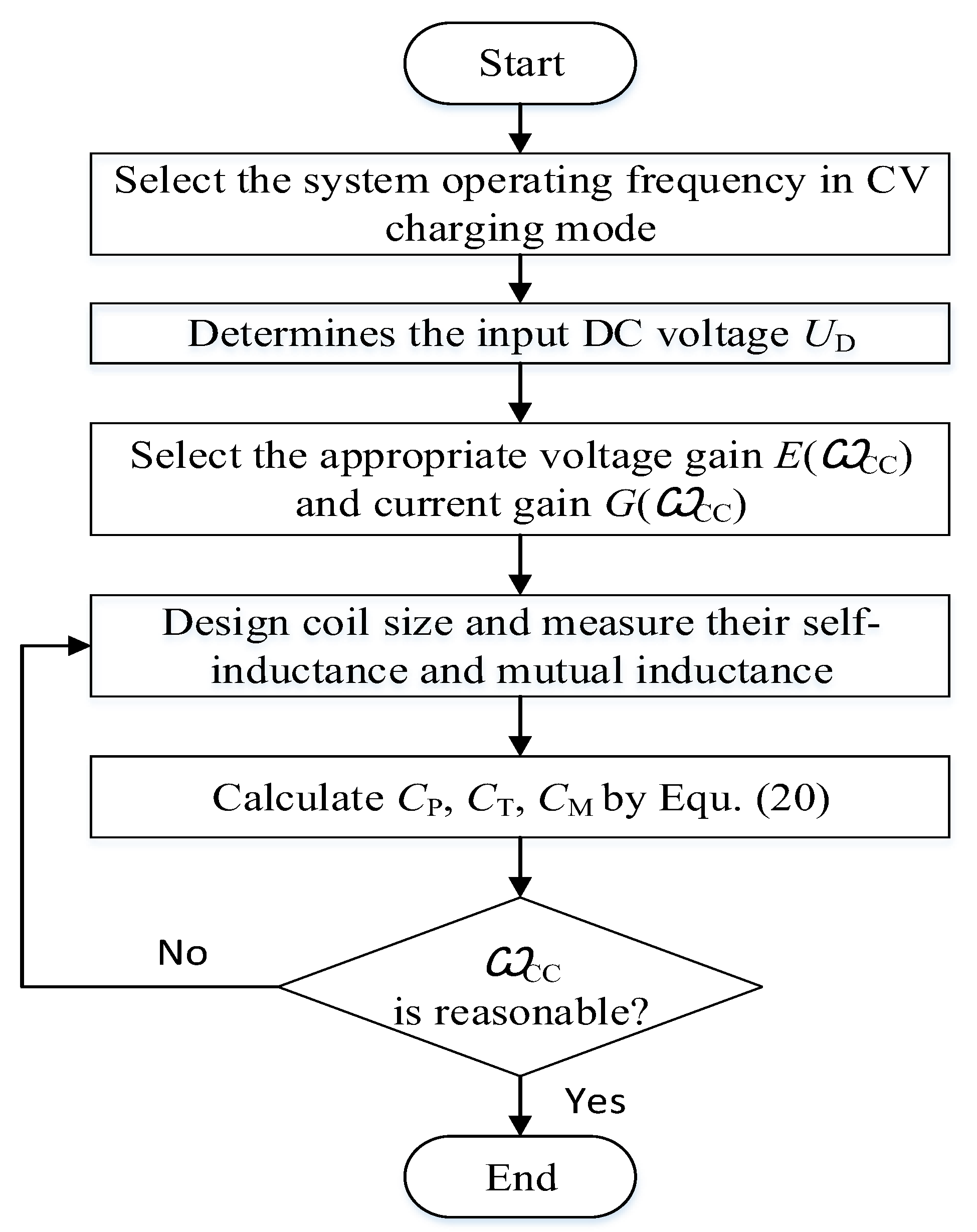
3.1. Design Ideas of the S/PS−Compensated WPT System

According to the analysis in Section 2, the satisfaction conditions for the system to operate in different modes of CC and CV, respectively, can be obtained. The general approaches of the design of the component parameters of the S/PS−compensated WPT system are summarized in Figure 4. In this paper, the CV operating frequency is first determined to be 85 kHz which satisfies most applications, and the input DC voltage is chosen to be 40 V. According to the charging demand of the battery load, the voltage gain E(ωcv) and the transconductance gain G(ωcc) are determined to be 1.5 and 0.05, respectively. Then, the size and geometry of the primary−side/secondary−side coils are determined based on factors such as space layout and power level. Subsequently, by using the magnetic field simulation software, the reference values of the primary−side self−inductance LP, the secondary−side self−inductance LS and the mutual inductance M between them can be estimated. Finally, the theoretical values of the compensation elements are calculated by substituting (20) and determines whether ω_cc is reasonable. An optimal solution is eventually chosen to determine the theoretical values.

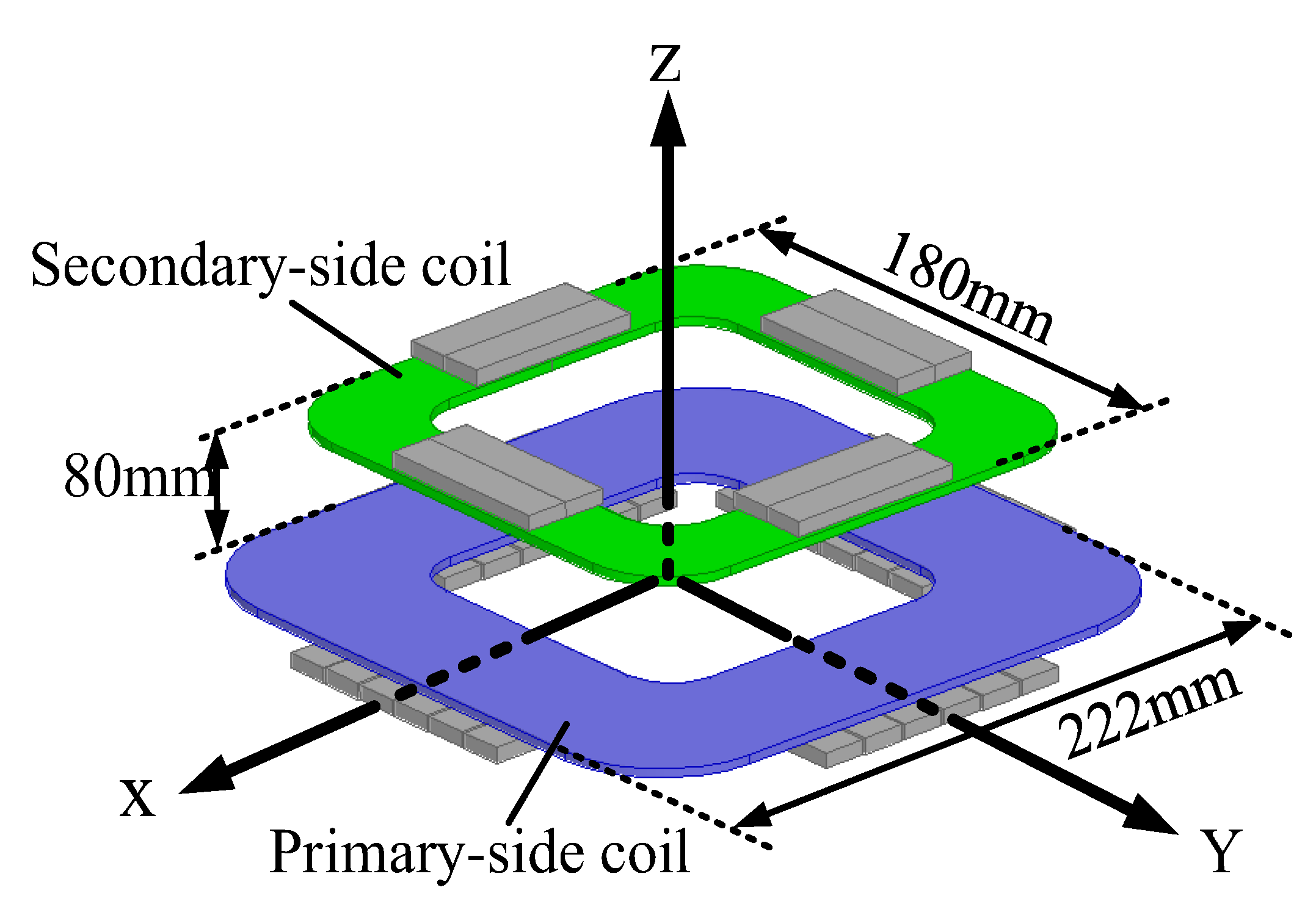
3.2. Design of the Loosely Coupled Transformer and Compensation Elements

According to [29], the square rounded corner design allows the coil to have greater self and mutual inductance, reducing the effects of skin and proximity effects. Litz wire has the advantage of having a small equivalent series resistance at high frequencies, which reduces the power loss of the system. Therefore, the Litz wire (400 strands, 2.88 mm diameter) was chosen for this paper to be designed using a square rounded structure and coupling was enhanced by placing a ferrite under the coil. The dimensional specifications of the magnetically coupled transformer selected for the system are shown in Table 1, with a distance of 80 mm between the two coils.
The finite element analysis (FEA) model of the loosely coupled transformer is displayed in Figure 5. The simulation results show that the self−inductances of the primary−side coil and the secondary−side coil are 30 μH and 106.82 μH, respectively, and the mutual inductance between the primary−side coil and the secondary−side coil is 20 μH.
According to the FEA simulation results, the theoretical value of the compensation capacitor can be obtained by substituting the coil simulation value and the set charging frequency of the CV mode into the (20). Then, according to the design approaches of the system parameters proposed in Figure 4, the theoretical values involved in the system parameters are summarized in Table 2.

3.3. Preliminary Simulation Verification

In order to initially verify the correctness of the theoretical analysis, the equivalent models in CC and CV modes are established in this paper using Matlab software, respectively. The theoretical values of the system obtained from the above analysis are substituted into the established simulation model, and the simulation results are obtained under the load of 10 Ω, 20 Ω, 40 Ω and 50 Ω, and the simulation results are shown in Figure 6.
According to Figure 6, there are two frequency points (65.15 kHz and 85 kHz) where the total input impedance is purely resistive at different load resistances. By comparing the total input impedance and voltage gain with the frequency sweep curve, it can be found that the voltage gain E(ωcv) is 1.5 for different load resistors at 85 kHz. Therefore, with a certain input voltage, it is possible to obtain load−independent CV output and the ZPA operation in CV mode.
Similarly, according to Figure 7, it can be easily found that the transconductance gain G(ωcc) of the system is also a constant value at another ZPA frequency point (65.15 kHz) under different load resistance conditions. As a result, with a certain input voltage, it is possible to achieve load−independent CC output and the ZPA operation in CC mode.
Based on the above analysis, Figure 6 and Figure 7 separately verify that the S/PS−compensated WPT system can realize CC and CV charging output unaffected by load changes at two different ZPA frequency points, respectively. Therefore, combining the above analysis, a frequency switching module can be added to the S/PS−compensated WPT system to satisfy the complete charging process of the battery.

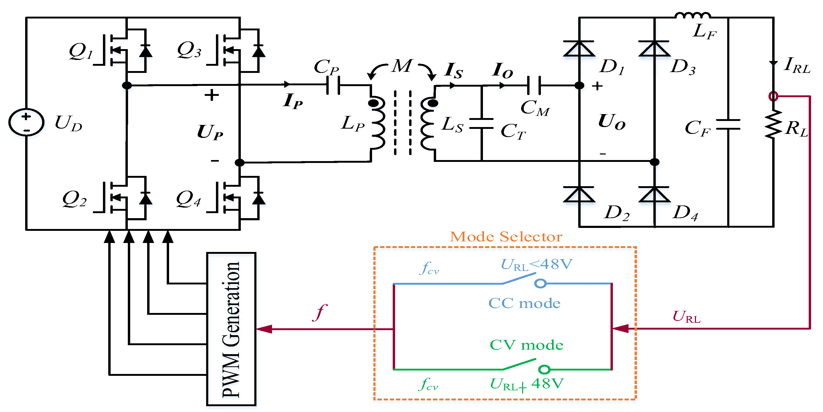
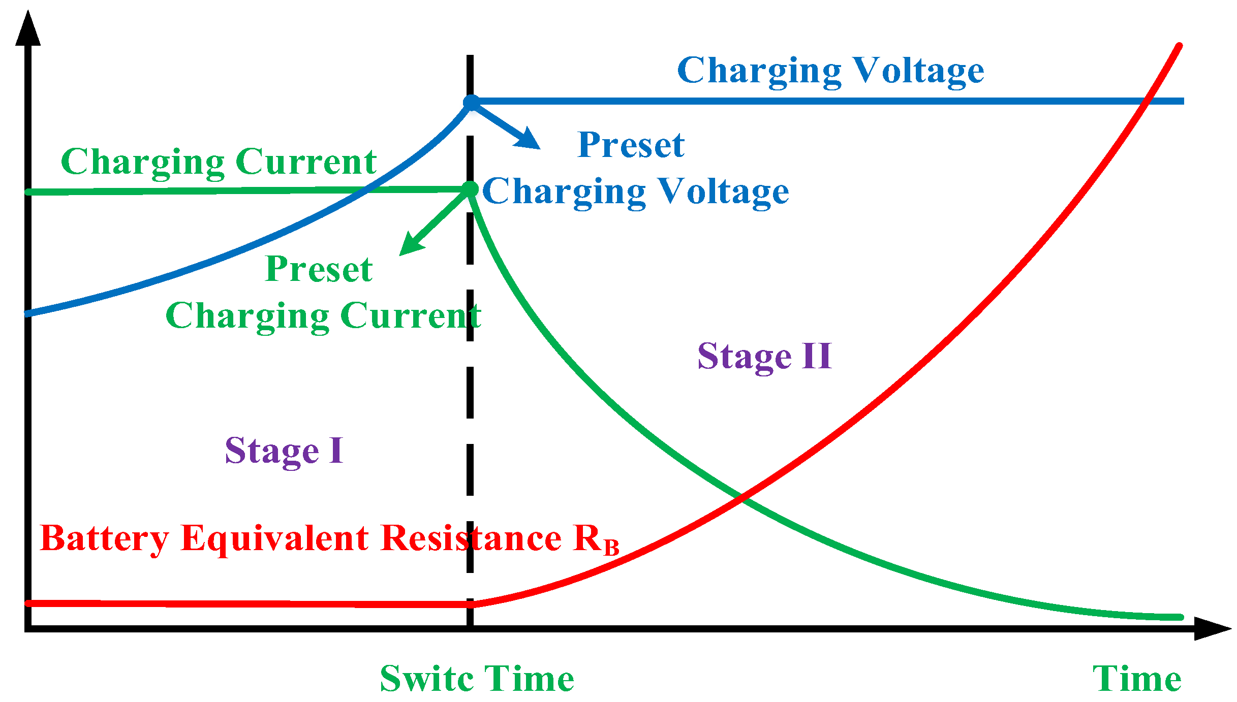
4. Design of the Switch Strategy of the S/PS−Compensated WPT System

The S/PS−compensated WPT system can satisfy the CC and CV outputs at two different ZPA operating frequencies (65.15 kHz and 85 kHz) without the need for a closed−loop controller, as verified above. The system switching strategy from CC mode to CV mode is shown in Figure 8. The switching strategy contains a CC mode selection switch in the blue part and a CV mode selection switch in the green part. By testing the charging voltage of the battery load, when the voltage URL rises to the preset voltage 48 V, the mode selector starts to act and the system switches from CC mode to CV mode for subsequent constant voltage charging. According to the above switching principle, the proposed system can meet the entire charging process of the battery as shown in Figure 1.

5. Experimental Results

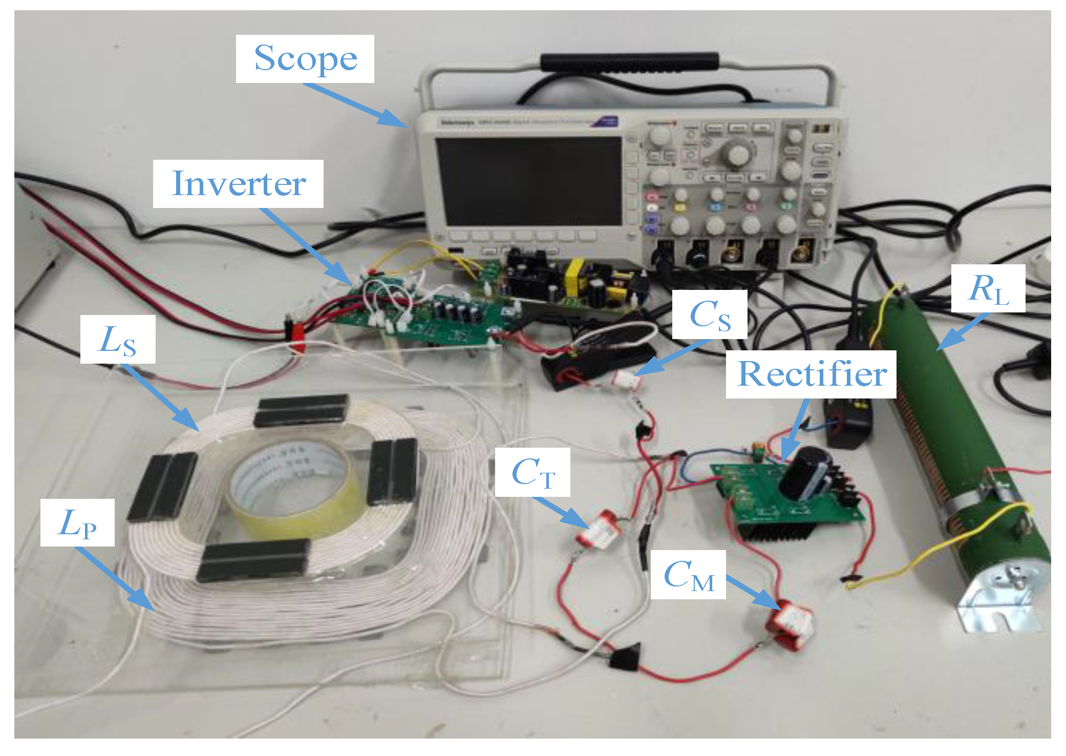
5.1. Experimental Model Construction

In order to further and more authoritatively verify the correctness and practicability of the proposed S/PS−compensated WPT system, a confirmatory experimental prototype is built based on Figure 8, as shown in Figure 9. The actual measured parameter values of each component of the experimental prototype are listed in Table 3. The input DC voltage is 40 V, and charging current in CC mode and the charging voltage in CV mode are set as 2 A and 48 V, respectively. Four Power MOSFETs (IRF530) with low on−resistance are selected to form the full−bridge HFI and four fast recovery diodes (MBR16100CT) with low turn−on voltage drop are adopted to form the full−bridge uncontrollable rectifier. The compensation capacitors of the system are polypropylene film capacitors, which can reduce the losses of the system. and other units are marked in Figure 9.

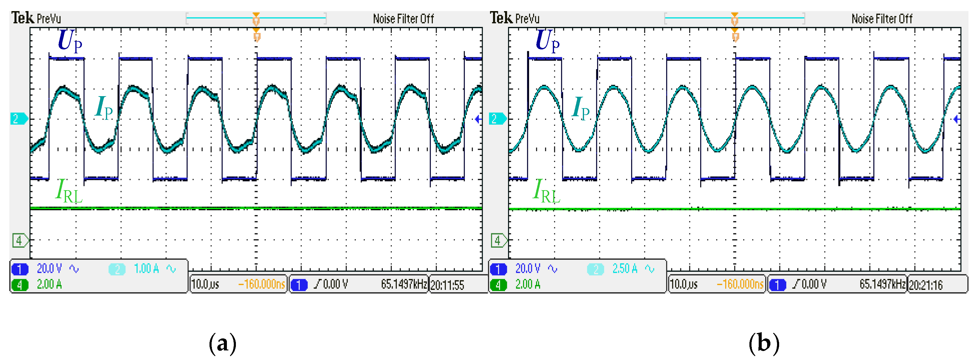
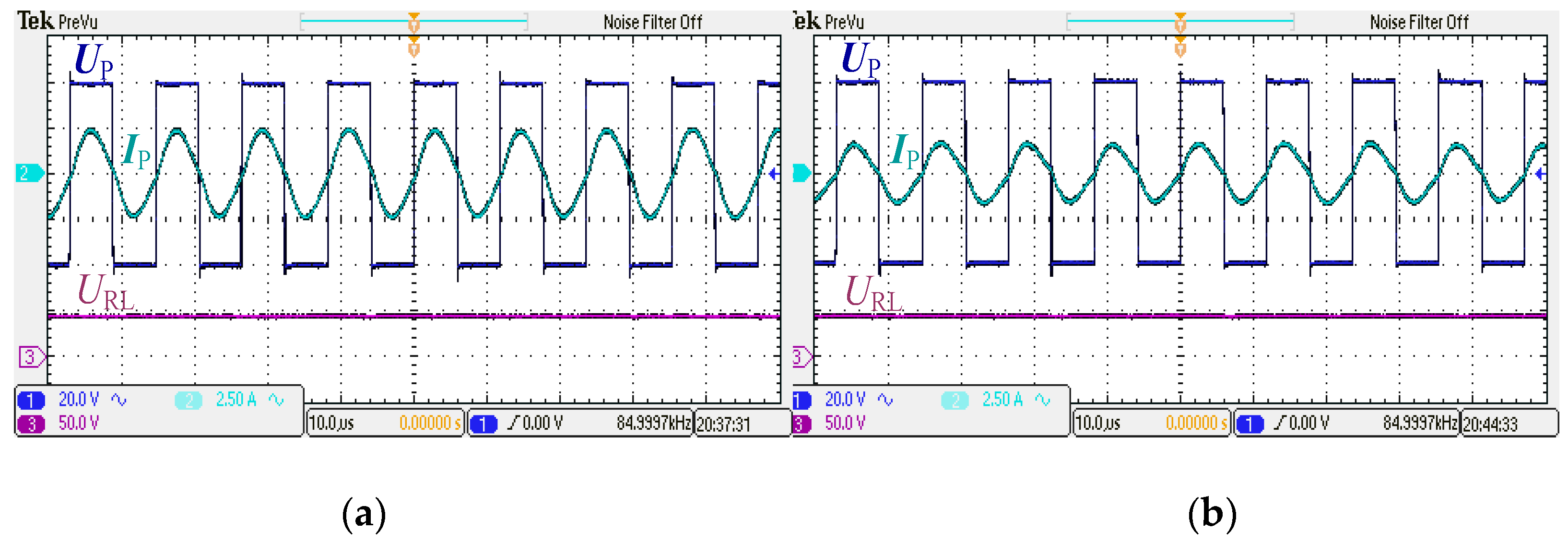
5.2. Experimental Results and Analysis

In this section, the CC and CV output characteristics of the S/PS−compensated WPT system are experimentally verified at two different ZPA operating frequencies, respectively. Firstly, when the input DC voltage UD of the system is 40 V and operating frequency is 65.15 kHz, the experimental verification in CC mode is carried out under the load of 5 Ω and 15 Ω respectively. The experimental waveforms of its inverter output voltage UP, inverter output current IP and the system charging current IRL are shown in Figure 10.
As evident from Figure 10, the system charging current in CC mode is always maintained at the constant value of 2 A at different load resistances. In addition, the inverter output voltage UP and the inverter output current IP are always in phase, which verifies the realization of ZPA operation under different load conditions and ensures the high efficiency of the system in CC mode.
The experimental verification in CV mode with the operating frequency of 85 kHz is carried out under the load of 40 Ω and 60 Ω respectively. The experimental waveforms of its inverter output voltage UP, inverter output current IP and the system charging voltage URL are shown in Figure 11.
As evident from Figure 11, the system charging voltage in CV mode is always maintained at the constant value of 48 V at different load resistances. In addition, the inverter output voltage UP and the inverter output current IP are always in phase, which demonstrates implementation of ZPA operation under different load conditions and guarantees the high efficiency of the system in CV mode.
Figure 12 shows the power transfer efficiency profile of the S/PS−compensated WPT system throughout the charging process. The red part of the power transfer curve represents that the proposed system works in CC mode (6 Ω~24 Ω), and the blue part of the power transfer efficiency curve stands for the proposed system works in CV mode (24 Ω~240 Ω). The overall transfer efficiency of the system presents a trend of first increasing and then decreasing. At CC mode, the system power transfer efficiency rises from 84.13% to peak value. At CV mode, the power transfer efficiency of the system ranges from 88.21% to 92.48%. The system power transfer efficiency is always maintained above 88% during the entire charging process, ensuring the high efficiency of the proposed S/PS−compensated WPT system.
To more intuitively reflect the superiority of the proposed S/PS−compensated WPT system, the performance comparison results of this study with previous similar studies are provided in Table 4. The advantages of the proposed system are summarized as follows:
(1).
Through reasonable parameter design, the proposed S/PS−compensated WPT system is able to achieve CC mode and CV mode charging by frequency switching. Importantly, the proposed system can realize ZPA operation in both CC mode and CV mode, ensuring the high efficiency of system, which is the advantage of this study compared with [24].
(2).
Both the number of coils and compensation elements in this study are relatively small, improving the cost, weight and volume of the system, which is superior to [25,26,27,28].

6. Conclusions

In order to meet the needs of battery charging, a new S/PS−compensated WPT system is proposed in this study. Through reasonable parameter design, the proposed system can realize the load−independent CC and CV charging output functions at two different frequency points, respectively. In addition, the ZPA operation during the whole charging process can be perfectly realized, ensuring the high efficiency of the system. The detailed and specific parameter design method for the proposed system to achieve CC and CV charging modes with related ZPA operation is provided. The unique feature of this system is that it can switch from CC to CV mode by frequency switching between two fixed frequencies (65.15 kHz and 85 kHz) without complex control techniques. It is worth mentioning that the number of coils and compensation components in this study is relatively small, only three compensation capacitors and no bulky compensation inductor, compared with the previous similar studies, the structural characteristics of the system have been improved. The experimental results fully verify the comprehensive performance of the proposed S/PS−compensated WPT system, which is in perfect agreement with the theoretical analysis. It is worth mentioning that this method is applicable to static charging with constant coupling coefficient, and has the simple and compact structure, which has certain potential application value.

Author Contributions

Conceptualization, L.Y. and Z.G.; methodology, L.Y.; software, S.J. and C.W.; validation, L.Y. and Z.G.; formal analysis, S.J. and C.W.; investigation L.Y. and Z.G.; data curation, C.W.; writing—original draft preparation, Z.G.; writing—review and editing, L.Y.; supervision, L.Y. All authors have read and agreed to the published version of the manuscript.

Funding

This research was funded by the National Natural Science Foundation of China under Grant 52177004 and U1904182 and Doctor Initiative Foundation of Henan Normal University under Grant 5101239170017.

Data Availability Statement

Not applicable.

Conflicts of Interest

The authors declare no conflict of interest.

References

  1. Li, S.; Mi, C.C. Wireless power transfer for electric vehicle applications. IEEE J. Emerg. Sel. Top. Power Electron. 2015, 3, 4–17. [Google Scholar]
  2. Yang, L.; Shi, Y.Y.; Wang, M.; Ren, L. Constant voltage charging and maximum efficiency tracking for WPT systems employing dual-side control scheme. IEEE J. Emerg. Sel. Top. Power Electron. 2021, 10, 945–955. [Google Scholar] [CrossRef]
  3. Liu, S.; Li, X.M.; Yang, L. A three-coil structure based WPT system design for the electric bike CC and CV charging without communication. IET Electr. Power Appl. 2019, 13, 1318–1327. [Google Scholar] [CrossRef]
  4. Zucca, M.; Cirimele, V.; Bruna, J.; Signorino, D.; Laporta, E.; Colussi, J.; Alonso Tejedor, M.A.; Fissore, F.; Pogliano, U. Assessment of the overall efficiency in WPT stations for electric vehicles. Sustainability 2021, 13, 2436. [Google Scholar] [CrossRef]
  5. Li, Y.; Zhang, S.; Cheng, Z. Double-coil dynamic shielding technology for wireless power transmission in electric vehicles. Energies 2021, 14, 5271. [Google Scholar] [CrossRef]
  6. Kim, J.; Marin, G.; Seo, J.M.; Neviani, A. A 13.56 MHz reconfigurable step-up switched capacitor converter for wireless power transfer system in implantable medical devices. Analog. Integr. Circuits Signal Processing 2022, 110, 517–525. [Google Scholar] [CrossRef]
  7. Xiao, C.; Cheng, D.; Wei, K. An LCC-C compensated wireless charging system for implantable cardiac pacemakers: Theory, experiment and safety evaluation. IEEE Trans. Power Electron. 2018, 33, 4894–4905. [Google Scholar] [CrossRef]
  8. Zhang, K.; Zhang, X.; Zhu, Z.; Yan, Z.; Song, B.; Mi, C.C. A new coil structure to reduce eddy current loss of WPT systems for underwater vehicles. IEEE Trans. Veh. Technol. 2019, 68, 245–253. [Google Scholar] [CrossRef]
  9. Yan, Z.; Zhang, Y.; Kan, T.; Lu, F.; Zhang, K.; Song, B.; Mi, C.C. Frequency optimization of a loosely coupled underwater wireless power transfer system considering eddy current loss. IEEE Trans. Ind. Electron. 2019, 66, 3468–3476. [Google Scholar] [CrossRef]
  10. Hui, S.Y. Planar wireless charging technology for portable electronic products and qi. Proc. IEEE 2013, 101, 1290–1301. [Google Scholar] [CrossRef] [Green Version]
  11. Kuncoro, C.; Luo, W.; Kuan, Y. Eco-green portable wireless power charger design with low-voltage, high-current fuel cell power source features. Int. J. Energy Res. 2020, 44, 9629–9645. [Google Scholar] [CrossRef]
  12. Cai, C.; Wang, J.; Zhang, F.; Liu, X.; Zhang, P.; Zhou, Y.G. A multichannel wireless UAV charging system with compact receivers for improving transmission stability and capacity. IEEE Syst. J. 2022, 16, 997–1008. [Google Scholar] [CrossRef]
  13. Cai, C.; Wang, J.; Wang, L.; Yuan, Z.; Tang, N.; Han, X.; Wang, S. Improved coplanar couplers based WPT systems for adaptive energy harvesting on power towers. IEEE Trans. Electromagn. Compat. 2021, 63, 922–934. [Google Scholar] [CrossRef]
  14. Cai, C.; Saeedifard, M.; Wang, J.; Zhang, P.; Zhao, J.; Hong, Y. A cost-effective segmented dynamic wireless charging system with stable efficiency and output power. IEEE Trans. Power Electron. 2022, 37, 8682–8700. [Google Scholar] [CrossRef]
  15. Huang, Z.; Wong, C.; Tse, K. An Inductive-Power-Transfer Converter with High Efficiency Throughout Battery-Charging Process. IEEE Trans. Power Electron. 2019, 34, 10245–10255. [Google Scholar] [CrossRef]
  16. Wang, X.; Xu, J.; Mao, M.; Ma, H. An LCL-based SS compensated WPT converter with wide ZVS range and integrated coil structure. IEEE Trans. Ind. Electron. 2021, 68, 4882–4893. [Google Scholar] [CrossRef]
  17. Sohn, Y.H.; Choi, B.H.; Lee, E.S.; Lim, G.C.; Cho, G.H.; Rim, C.T. General unified analyses of two-capacitor inductive power transfer systems: Equivalence of current-source SS and SP compensations. IEEE Trans. Power Electron. 2015, 30, 6030–6045. [Google Scholar] [CrossRef]
  18. Qu, X.; Han, H.; Wong, S.C.; Chi, K.T.; Chen, W. Hybrid IPT topologies with constant current or constant voltage output for battery charging applications. IEEE Trans. Power Electron. 2015, 30, 6329–6337. [Google Scholar] [CrossRef]
  19. Xu, Z.; Yang, L.; Li, X.; Liu, S.; Dong, Z.; Wu, Y. Analysis and design of a S/PS-compensated IPT system with constant current output. IET Electr. Power Appl. 2020, 14, 2739–2749. [Google Scholar] [CrossRef]
  20. Li, X.; Yang, L.; Xu, Z.; Hu, J.; He, Z.; Mai, R. A communication-free WPT system based on transmitter-side hybrid topology switching for battery charging applications. AIP Adv. 2020, 10, 45302. [Google Scholar] [CrossRef] [Green Version]
  21. Li, Y.; Xu, Q.; Lin, T.; Hu, J.; He, Z.; Mai, R. Analysis and design of load-independent output current or output voltage of a three-coil wireless power transfer system. IEEE Trans. Transp. Electrif. 2018, 4, 364–375. [Google Scholar] [CrossRef]
  22. Li, G.; Kim, D.-H. A Wireless Power Transfer Charger with Hybrid Compensation Topology for Constant Current/Voltage Onboard Charging. Appl. Sci. 2021, 11, 7569. [Google Scholar] [CrossRef]
  23. Chen, Y.; Kou, Z.; Zhang, Y.; He, Z.; Mai, R.; Cao, G. Hybrid topology with configurable charge current and charge voltage output-based WPT charger for massive electric bicycles. IEEE J. Emerg. Sel. Top. Power Electron. 2018, 6, 1581–1594. [Google Scholar] [CrossRef]
  24. Huang, Z.; Wong, S.-C.; Tse, C. Design of a single-stage inductive-power-transfer converter for efficient EV battery charging. IEEE Trans. Veh. Technol. 2017, 66, 5808–5821. [Google Scholar] [CrossRef]
  25. Vu, V.B.; Tran, D.H.; Choi, W. Implementation of the constant current and constant voltage charge of inductive power transfer systems with the double-sided LCC compensation topology for electric vehicle battery charge applications. IEEE Trans. Power Electron. 2017, 33, 7398–7410. [Google Scholar] [CrossRef] [Green Version]
  26. Qu, X.; Chu, H.; Wong, S.C.; Chi, K.T. An IPT battery charger with near unity power factor and load-independent constant output combating design constraints of input voltage and transformer parameters. IEEE Trans. Power Electron. 2019, 34, 7719–7727. [Google Scholar] [CrossRef]
  27. Yang, L.; Li, X.; Liu, S.; Xu, Z.; Cai, C.; Guo, P. Analysis and design of three-coil structure WPT system with constant output current and voltage for battery charging applications. IEEE Access 2019, 7, 87334–87344. [Google Scholar] [CrossRef]
  28. Tran, D.H.; Vu, V.B.; Choi, W. Design of a high-efficiency wireless power transfer system with intermediate coils for the on-board chargers of electric vehicles. IEEE Trans. Power Electron. 2017, 33, 175–187. [Google Scholar] [CrossRef]
  29. Yang, L.; Li, X.; Liu, S.; Xu, Z.; Cai, C. Analysis and design of an LCCC/S-compensated WPT system with constant output characteristics for battery charging applications. IEEE J. Emerg. Sel. Top. Power Electron. 2021, 9, 1169–1180. [Google Scholar] [CrossRef]
Figure 1. Typical charging profile of the Li-ion battery.
Electronics 11 01488 g001
Figure 2. Circuit diagram of the S/PS−compensated WPT System.
Electronics 11 01488 g002
Figure 3. Equivalent circuit of the S/PS−compensated WPT System.
Electronics 11 01488 g003
Figure 4. Design approaches of the S/PS−compensated WPT system.
Electronics 11 01488 g004
Figure 5. Experimental model of the loosely coupled transformer.
Electronics 11 01488 g005
Figure 6. Voltage gain and phase of input impedance of the S/PS−compensated WPT system.
Electronics 11 01488 g006
Figure 7. Transconductance gain and phase of input impedance of the S/PS−compensated WPT system.
Electronics 11 01488 g007
Figure 8. Switch strategy of the S/PS−compensated WPT system.
Electronics 11 01488 g008
Figure 9. Experimental model of the S/PS−compensated WPT system.
Electronics 11 01488 g009
Figure 10. Experimental waveforms of UP, IP and IRL in CC charging mode. (a) RL = 5Ω (b) RL = 15 Ω.
Electronics 11 01488 g010
Figure 11. Experimental waveforms of UP, IP and URL in CV charging mode. (a) RL = 40 Ω (b) RL = 60 Ω.
Electronics 11 01488 g011
Figure 12. The power transfer efficiency profile of the S/PS−compensated WPT system.
Electronics 11 01488 g012
Table 1. Physical parameters of the LCT.
ParametersPrimary−SideSecondary−Side
Coil outer diameter222 mm180 mm
Coil inner diameter180 mm120 mm
Turns1710
Table 2. Theoretical parameters of the proposed S/PS−compensated WPT system.
ParametersTitle 2ParametersTitle 3
ωcv85 kHzCP47.17 nF
ωcc65.15 kHzCM81.26 nF
UD40 VCT116.86 nF
LP30 μHG(ωcc)0.05
LS106.82 μHE(ωcv)1.5
M20 μHIO2 A
RP/RS0.1 Ω/0.05 ΩUO60 V
Table 3. Measured parameter values of the S/PS−compensated WPT system.
ParametersTitle 2ParametersTitle 3
ωcv85 kHzCP47.85 nF
ωcc65.15 kHzCM82.34 nF
UD40 VCT117.66 nF
LP107.73 μHG(ωcc)0.05
LS31.56 μHE(ωcv)1.5
M21.22 μHIO2 A
RP/RS0.1 Ω/0.05 ΩUO48 V
Table 4. Comparison of this study with previous similar studies.
Proposed inRef. [24]Ref. [25]Ref. [26]Ref. [27]Ref. [28]This Study
Number of coils222342
Resonant tankSSLCC/LCCLCC/LCCThree−coilFour−coilS/PS
Number of primary−side compensation components133221
Number of secondary−side compensation components133122
Frequency in CC mode (kHz)50.1168206.668.25065.15
Frequency in CV mode (kHz)70.0979.1259.98559.485
ZPA in CC modeYesYesYesYesYesYes
ZPA in CV modeNoYesYesYesYesYes
Compact and lightweight secondary−sideYesNoNoYesNoYes
Publisher’s Note: MDPI stays neutral with regard to jurisdictional claims in published maps and institutional affiliations.

