1. Introduction
Analogue-to-digital converters (ADCs) are divided into two types: linear and nonlinear. Almost all nonlinear ADCs are logarithmic. Each ADC type is divided into three classes: incremental, with successive approximation, and parallel. Combined ADCs contain two classes of converters; their properties are completely determined by the properties of the converters used in them. Therefore, such a class is usually not considered separately.
1.1. Logarithmic ADCs
Logarithmic ADCs (LADCs) are traditionally divided into the classes of incremental, with successive approximation, and parallel. In recent years, a new class—recursive—has been developed [
1,
2,
3,
4,
5,
6,
7,
8,
9,
10,
11,
12,
13,
14,
15,
16,
17,
18,
19,
20,
21,
22].
Among logarithmic ADCs (LADCs), incremental converters [
1,
2,
3,
4,
7,
8,
9,
12,
15,
20] are the most commonly used due to their simpler implementation.
Prominent among them are Pipeline LADCs [
1,
2,
3,
4] due to their fabrication as integrated circuits and LADCs on switched capacitors with charge accumulation [
7,
8,
9,
12,
15], in which any value of the logarithm base is easily set—a feature desirable in a wide variety of applications.
In papers [
2,
3,
4], the Pipeline LADCs described are realized as integrated circuits with 8 bit output code and low power consumption, amounting to dozens of microwatts.
Paper [
5] discusses LADCs with current input and temperature compensation, together with automatic calibration of the offset voltage with 8 bit output code. The principle of operation is p-n junction of a semiconductor diode.
Patent [
19] describes an LADC that uses double integration to improve accuracy.
Patent [
20] describes an LADC for which the operating principle is based on the discharge of a capacitor in an RC circuit. A large measurement range is obtained by placing an amplifier between the capacitor and the comparator. The mathematical compensation of errors of the time constant of the RC circuit and offset voltage is presented; therefore, two reference voltage values were measured earlier.
Papers [
7,
8,
9,
12] developed principles for operating and modelling LADCs on switched capacitors with charge accumulation and impulse feedback, and patent [
15] proposed a way to improve the accuracy.
LADCs with successive approximation are described in papers [
7,
10,
11,
13,
22].
These papers present the developed principles of operation, design, error analysis, and modelling of LADCs on switched capacitors with successive approximation.
Recursive LADCs occupy an intermediate position between incremental LADCs and LADCs with successive approximation in terms of the conversion speed. Compared to the latter, they have slightly lower speed, but outperform them with fewer reference voltages needed for conversion.
Patent [
14] proposes a way to increase the accuracy and simplify the implementation of an LADC by using a recursive algorithm of the operation.
In patent [
16], considering the use of the recursive conversion method, the accuracy and speed of the LADC were improved.
In patent [
21], the use of a neural network that employs a recursive algorithm is proposed to increase the speed of analogue-to-digital conversion.
It is generally known that parallel linear ADCs have the highest conversion speed. Implementation of parallel logarithmic ADCs was practically impossible due to the increase in reference error of the voltage divider. To counter this drawback, it has been proposed to implement a voltage divider using equal blocks of resistors or capacitors instead of equal resistors [
17,
18].
Since incremental LADCs are very slow, and parallel LADCs are very complex, a trade-off between sufficient accuracy and speed must be sought in LADCs with successive approximation.
1.2. Linear ADCs
The most common ADCs are linear ADCs with successive approximation and incremental ADC with integration. They account for about 95% of all existing ADCs. ADCs with successive approximation occupy an intermediate position between parallel (flash) ADCs and incremental ADCs in such important parameters as accuracy and conversion speed, resulting in their wider application.
In [
23], the architecture of a linear ADC converter with indirect voltage–time processing was proposed. Time is then quantized by simple functional nodes. To increase the speed of the comparators, the low-level signals are amplified by Dickson charge pumps. A prototype of such an ADC was implemented and the results of its experimental research were presented.
The work [
24] is an article on charge pumps for ultra-low-power applications. The manual introduces the most modern integrated topologies. Recommendations are given for the selection of the optimal solution for given design requirements.
A linear ADC was used in [
25], which uses a Dickson charge pump for voltage–time conversion. Time is quantized with low-complexity digital circuits without the use of analog amplifiers or current sources. Data for the verification of the characteristics of three ADC prototypes are given.
In [
26], SAR ADCs were synthesized using only standard digital circuits. This implementation facilitates the integration of ADCs with various functional units that require testing and diagnosis. Non-linearity is compensated by calibration based on the histogram. The technique of pre-sampling with the method of redundant error correction is used to implement an ADC without a sample/hold (S/H) scheme. The technical characteristics of the proposed ADC converter, produced with 28 nm CMOS technology, are given.
Ref. [
27] presents a simple design method for increasing the energy efficiency of linear charge pumps. The clock signal amplitude below the supply voltage is used to reduce power consumption during processing. Increasing the number of stages of the charge pump ensures a constant rated output voltage.
This paper proposes a method for constructing LADCs with successive approximation on switched capacitors (SC), in which the logarithm base in the conversion process is changed to improve accuracy. The essence of this method is that the value of the logarithm base changes in each successive tact of conversion of the converter, while the compensation voltage is formed as the product of the reference voltage and the value of the logarithm base of those tacts in which the compensation voltage exceeded the input voltage.
The weights of the individual nodes of the voltage divider can be determined on a binary basis, i.e., as power functions based on a binary code, and thus provide a representation of the conversion result in the form of a binary code. Such presentation of the result is convenient for logging, storing, and further processing.
The novelty of the present article in comparison to publications [
10,
11,
22] is that: (1) in order to increase the accuracy, a method of construction of the LADC converter with a change of the base of the logarithm in the conversion process is proposed, with the simultaneous improvement of analog switches (by reducing their resistance in the state of turned on); (2) electrical models of such LADC transducers and mathematical models of their errors are developed, and the estimation of these errors is given.
The aim of this paper is to develop mathematical models of LADC errors with successive approximation on switched capacitors with a variable logarithm base, and to evaluate these errors and the accuracy of LADCs considering the parameters of modern components.
In this study, we used the methods of computer modeling and computer experiment to study the errors and the equations that we derived from the well-known laws of electrical engineering and electrostatics.
The developed models concern the implementation of the LADC proposed by us with successive approximation, the block diagram of which is presented in a simplified manner in
Figure 1 and is an improvement of the LADC implementation given in [
22]. The improvement is to increase the accuracy of our proposed LADC building method by changing the logarithm base in the processing process, whilst simultaneously improving the analog keys by reducing their on-state resistance.
2. Physical Model of the LADC with Successive Approximation on Switched Capacitors with a Variable Logarithm Base
A simplified functional diagram of the LADC with a successive approximation on switched capacitors with a variable logarithm base is given in
Figure 1, where WO—operational amplifier; F
T—tact frequency;
NC—control code; WN—voltage follower; RWS—adjustable scaling amplifier; K
M—comparator; RKP—successive approximation register (SAR); K0–K4—analogue keys;
C1 and
C2—first and second capacitor; and
Ur,
Uc, and
Uin—reference, control, and input voltages, respectively.
Our LADC with successive approximation on switched capacitors includes both digital and analogue components.
In fact, the accuracy of the LADC is only affected by its analogue components, including capacitors, keys, adjustable scaling amplifier, reference voltage source, and a comparator.
Note that when making a reference voltage source (Ur), using modern components with precision Zener diodes, a reference voltage error within 0.001% can be easily achieved. Therefore, this error will be ignored hereafter.
The compensation voltage of the LADC with successive approximation arises at the output of the adjustable scaling amplifier block and is applied to one of the comparator inputs via a voltage follower.
The values of the transfer coefficients of the adjustable scaling amplifier are given for each
i-th tact of conversion according to the formula
which means that
where
—ideal value of the logarithm base and
n—number of the output bit of the LADC code, with
corresponding to more significant bit and
to the less significant bit.
The compensation voltage of the LADC changes as an exponential function according to the formula
where
Ai—coefficient that reaches the value of 1 or 0 depending on the result of comparing the compensation voltage and input voltage in the comparator.
The ideal conversion characteristic of the LADC with successive approximation on switched capacitors has the following form:
that is,
The actual conversion characteristics of the LADC differ from the ideal one due to the influence of parasitic parameters of the diagram components, including:
- (1)
parasitic capacitances;
- (2)
leakage currents;
- (3)
non-ideality of the comparator and the adjustable scaling amplifier.
The effect of component non-ideality causes the voltage level on capacitors C1 and C2 to change, resulting in a conversion error.
The effect of the input currents and parasitic capacitances of the comparator and the adjustable scaling amplifier is negligibly small because the voltage follower is placed before them.
The offset voltage can also be negligible, since it can be minimized to practically zero by automatic correction.
It can be concluded that accounting for non-ideality of components of the LADC with successive approximation on switched capacitors actually boils down accounting for the effect of parasitic capacitances of analogue keys, leakage currents of accumulation capacitors, and input voltage of the voltage follower on the LADC accuracy. The latter two factors can be omitted in a first approximation if precision elements (styroflex or polystyrene) are used as accumulation capacitors, and the voltage follower is implemented on an operational amplifier with a reduced input current (0.1 nA or less).
3. Mathematical Models of LADC Errors with Successive Approximation on Switched Capacitors
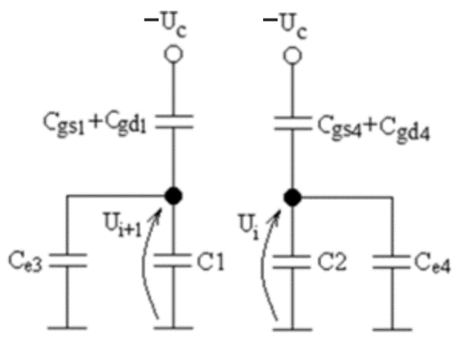
Based on the functional diagram of
Figure 1, a model of the LADC with successive approximation on switched capacitors was realized which takes into account the influence of parasitic capacitances. This model is shown in
Figure 2.
The influence of parasitic capacities manifests itself through
In the analysis of the LADC system, modern high-quality analogue keys that are made using field-effect transistors are considered.
The processes involved in the operation of the LADC are discussed below.
When the LADC is activated, key K0 is switched on and the voltage level is set on the accumulation capacitor
C1:
Then, conversion begins tact by tact, with each clock impulse corresponding to one tact of conversion.
In the first tact of conversion, keys K1 and K3 are switched on and the voltage level is set on the accumulation capacitor
C2:
With each clock impulse, the voltages on accumulation capacitors C1 and C2 change, with either capacitor being connected to the voltage follower input in sequence. As a result, all considerations that are valid for one capacitor will also be valid for the next clock impulse for the other capacitor.
3.1. First Tact of Conversion
3.1.1. Transfer of Parasitic Charge
A model of the LADC with successive approximation on switched capacitors which takes into account parasitic charge transfer is shown in
Figure 3, where
It should be noted that when the analogue key switches from the on state (high control voltage ) to the off state (low control voltage ), the parasitic charge that was accumulated by the parasitic capacitances of the gates of the field-effect transistors of the key during the operation of the control voltage impulse () is transferred to the accumulation capacitor associated with the key.
During the operation of the first clock impulse, the K3 key is switched on and a charge will accumulate on its gates:
where
At the end of the first clock impulse, the K3 key switches off and there will be a redistribution of this parasitic charge between the parasitic capacitance and the accumulation capacitor C2.
The summative charge is equal to
that is,
where
QC2—charge accumulated on capacitor
C2 and
Meanwhile, the summative charge after the first clock impulse can be represented as
where
U1q—voltage on accumulation capacitor
C2 after the first clock impulse.
By comparing the formulas above, we can obtain the value of the voltage on the accumulation capacitor
C2 when the charge redistribution is complete after the first tact of conversion:
Further, if we introduce the symbol
then the formula for the voltage on the accumulation capacitor
C2 taking into account the influence of the parasitic charge at the end of the first tact has the following form:
3.1.2. Control Voltage Transmission
A model of the LADC with successive approximation on switched capacitors which takes into account the control voltage transmission is shown in
Figure 4, where
The parasitic capacitance of the gate of key K4 and the accumulation capacitor
C2 form a capacitive voltage divider that divides the control voltage
Uy in proportion to the values of these capacitances. As a result, after the first clock tact, the voltage increase on the accumulation capacitor
C2 from the control voltage transmission will be equal to
where
Further, by introducing the symbol
we can obtain the voltage increase on the accumulation capacitor
C2 from the control voltage transmission
Uy:
Thus, after the first tact of conversion, the accumulation capacitor
C2 will be connected to the input of the voltage follower, and the voltage on it—taking into account parasitic charge transfer and control voltage transmission—is equal to
that is,
3.2. Second Tact of Conversion
In the second tact, capacitor C1 should be considered instead of C2, and key K1 instead of K4. Meanwhile, the parameters of the capacitors and keys should be assumed to be equal, respectively.
3.2.1. Transfer of Parasitic Charge
The parasitic charge after switching off key K2 is
The summative charge after the second clock impulse is equal to
By comparing the formulas above, and by introducing the symbol
We can obtain the voltage value on the accumulation capacitor
C1 taking into account the transfer of parasitic charge after the second tact:
that is,
3.2.2. Transmission of Control Voltage
The transmission of the control voltage after the second tact changes the voltage on the accumulation capacitor
C1 is
where
Thus, after the second tact, the accumulation capacitor
C1 will be connected to the input of the voltage follower, and the voltage on it—taking into account parasitic charge transfer and control voltage transmission—is equal to
that is,
Finally, the voltage on the accumulation capacitor
C1 after the second tact is
3.3. Third Tact of Conversion
Again, the accumulation capacitors swap places and the accumulation capacitor C2 is connected to the input of the voltage follower, which means that the same processes as in the first tact exist in the LADC.
3.3.1. Transfer of Parasitic Charge
The parasitic charge after the third tact is equal to
The summative charge after the third tact is equal to
By comparing the formulas above, we can obtain the value of voltage on the accumulation capacitor
C2 taking into account transfer of parasitic charge after the third tact:
that is,
3.3.2. Control Voltage Transmission
Change of the voltage on the accumulation capacitor
C2 in the third tact of conversion is analogous to the first tact. The voltage—including parasitic charge transfer and control voltage transmission—is equal to
that is,
Finally, the voltage on the accumulation capacitor
C2 after the third tact is
3.4. Fourth Tact of Conversion
For the fourth tact of conversion, we have
The formulas for the next tacts of conversion can be obtained analogously, taking into account the fact that the voltage on the accumulation capacitor is
- (a)
- (b)
in even tacts:
where
d = 5, 6, 7…
n.
3.5. Fifth Tact of Conversion
For the fifth tact of conversion, we have
3.6. Sixth Tact of Conversion
For the sixth tact of conversion, we have
3.7. Seventh Tact of Conversion
For the seventh tact of conversion, we have
3.8. Eighth Tact of Conversion
For the eighth tact of conversion, we have
where
n—
tact of conversion.Generally speaking, the voltage on the accumulation capacitor after the n-th tact of conversion is equal to
Finally, in the general case, the voltage on the accumulation capacitor after any
m-th tact of conversion is equal to
where
m = 1, 2, 3 …
n;
at
m = 1;
at
m > 1; and
The second and third section of this formula reflect the summative absolute error of conversion of the LADC with successive approximation on SC (
), which is due to the influence of parasitic capacitances of the LADC components after
m-tacts of conversion:
Considering the components of the summative absolute error
, with multipliers k
1 and k
2 from parasitic charge transfer (
) and with multipliers
and
from control voltage transmission (
), we have
According to these formulas, one can define the voltage on the accumulation capacitor and its error at any tact of conversion.
As can be seen from the last formula, the errors from parasitic charge transfer and control voltage transmission are to some extent mutually compensated because they have different signs.
The results from calculating the summative absolute error
, caused by the influence of parasitic capacitances of the LADC components, are given in
Figure 5 (for
C1 =
C2 = 10 nF) and
Figure 6 (for
C1 =
C2 = 1 nF).
Calculations were performed considering an input signal range of 1 mV–10 V, with the following assumptions:
From the analysis of the test results shown in
Figure 5 and
Figure 6, it can be seen that the summative error caused by the influence of parasitic capacitances of the LADC components
is positive and the absolute value does not exceed
- (A)
for
C1 =
C2 = 10 nF and 10, 12, and 16 bit LPAC, respectively:
- (B)
for
C1 =
C2 = 1 nF and 10, 12, and 16 bit LPAC, respectively:
4. Assessment of Accuracy of LADC with Successive Approximation on Switched Capacitors
Adding errors amounts to considering the presence of correlation between particular errors and organizing them into corresponding groups by correlation coefficient. The sum of two errors, including correlation, is defined according to the formula
where:
and
—first and second error, respectively, and
—correlation coefficient, which is equal to zero when there is no correlation between errors and equal to one when there is strong correlation.
It should also be noted that in order to determine the summative error, one should use collectively nominal errors as separate components.
The LADC summative error (
) is equal to the sum of instrumental and methodological errors, which are not correlated with each other. Therefore, the correlation coefficient takes the value of zero (
= 0), and the LADC summative error is defined by the equation
The instrumental error of LADC is determined by non-ideal components: voltage follower, adjustable scaling amplifier, comparator, reference voltage source, analogue keys, and capacitors C1 and C2.
Errors from the polarization voltage of the voltage follower, adjustable scaling amplifier, comparator, reference voltage source, and deviations from the nominal capacitance value of the capacitors
C1 and
C2 are compensated during the initial installation of the LADC according to recommendations given in [
9].
Errors from LADC leakage currents are negligibly small because high-quality components are used, whose leakage currents amount to hundreds of pA, with a relatively short time of conversion of 16 tacts.
Therefore, the instrumental error of the LADC with successive approximation on switched capacitors is reduced to the error from the influence of parasitic capacitances:
where
—rated input voltage.
Calculated according to the last formula, the relative summative errors of the LADC due to the influence of parasitic component capacitances () are positive and do not exceed
- (A)
for
C1 =
C2 = 10 nF and 10, 12, and 16 bit LADC, respectively:
- (B)
for
C1 =
C2 = 1 nF and 10, 12 and 16 bit LADC, respectively:
By setting the quantization error to (which is appropriate for 16 bit accuracy), with C1 = C2 = 10 nF and Cp = 1 pF, we can obtain the final error of the described LADC with successive approximation on switched capacitors according to Formula (1): .
5. Conclusions
From the conducted modelling of the LADC with successive approximation on switched capacitors with a variable logarithm base, we conclude the following:
The influence of parasitic capacitances of analogue keys on charge accumulation processes is manifested by
- (a)
transmission of the control voltage of the analogue keys into the capacitor cell;
- (b)
transfer of the parasitic charge of the gate of analogue keys to the capacitor cell.
The errors from the influence of parasitic capacitances of LADC components increase in absolute values along with the increase in the number of tacts of conversion. The largest error increments occur in the first two tacts of conversion; in subsequent tacts, the increments are negligibly small.
Errors from the influence of parasitic capacitances of LADC components decrease in absolute values as the capacitance of the capacitors (C1 and C2) of the capacitor cell increases and the number of LADC bits decreases.
Errors from parasitic charge transfer () are positive and errors from control voltage transmission () are negative, resulting in partial mutual compensation of the components of the summative error (), which becomes positive.
The instrumental error of the LADC is practically equal to the error from the influence of inter-electrode parasitic capacitances of components.
To achieve satisfactory accuracy for the 16 bit LADC, the capacitance of the capacitors (C1 and C2) of the capacitor cell must be at least 10 nF; for the 12 bit LADC, a capacitance of 1 nF is sufficient. These figures correspond to the usage of modern keys of manufacturers such as Maxim or Analog Devices with parasitic capacitance values less than 1 pF. Despite achieving high accuracy, the logarithmic ADC we propose has some shortcomings: a somewhat complicated diagram and relatively large capacities (1–10 nanofarads) of the capacitor cell.
Author Contributions
Conceptualization, Z.M., I.Z., L.M., A.S., Z.S. and H.Y.; methodology, Z.M., I.Z., L.M., A.S., Z.S. and H.Y; writing—original draft preparation, Z.M., I.Z., L.M., A.S., Z.S. and H.Y.; writing—review and editing, Z.M., I.Z., L.M., A.S., Z.S. and H.Y.; visualization, Z.M., I.Z., L.M., A.S., Z.S. and H.Y.; supervision, Z.M., I.Z., L.M., A.S., Z.S. and H.Y.; funding acquisition, A.S. and Z.S. All authors have read and agreed to the published version of the manuscript.
Funding
The research was carried out as part of the research work entitled ‘Analysis of the operation of power and control systems in the systems of the Industry 4.0 directive’, financed by 03.0.21.00/1.02.001 SUBB.EKUE. 22.001, Poland.
Conflicts of Interest
The authors declare no conflict of interest.
Abbreviations
| ADC | analogue-to-digital converter |
| LADC | logarithmic analogue-to-digital converter |
| LADC SA | logarithmic analogue-to-digital converter with successive approximation |
| SAR | successive approximation register |
| S/H | sample/hold |
| RC circuit | resistor–capacitor circuit |
| SC | switched capacitors |
| WO | operational amplifier |
| FT | tact frequency |
| NC | control code |
| WN | voltage follower |
| RWS | adjustable scaling amplifier |
| KM | comparator |
| K0–K4 | analogue keys |
| C1 and C2 | first and second capacitor |
| Ur | reference voltage |
| Uc | control voltage |
| Uin | input voltage |
| Cgs | gate–source capacitance |
| Cgd | gate–drain capacitance |
| Cds | drain–source capacitance |
| Cp | parasitic capacitance |
| summative absolute error |
| errors from parasitic charge transfer |
| errors from control voltage transmission |
| summative error of LADC |
| instrumental error of LADC |
References
- Lee, J.; Kang, J.; Park, S.; Seo, J.; Anders, J.; Guilherme, J.; Flynn, M.P. A 2.5 MW 80 DB DR 36 DB SNDR 22 MS/s Logarithmic Pipeline ADC. IEEE J. Solid-State Circuits 2009, 44, 2755–2765. [Google Scholar] [CrossRef]
- Guilherme, J.; Vital, J.; Franca, J. A True Logarithmic Analog-to-Digital Pipeline Converter with 1.5 Bit/Stage and Digital Correction. In Proceedings of the ICECS 2001 8th IEEE International Conference on Electronics, Circuits and Systems (Cat. No.01EX483), Malta, 2–5 September 2001; Volume 1, pp. 393–396. [Google Scholar]
- Sirimasakul, S.; Thanachayanont, A.; Jeamsaksiri, W. Low-Power Current-Mode Logarithmic Pipeline Analog-to-Digital Converter for ISFET Based PH Sensor. In Proceedings of the 2009 9th International Symposium on Communications and Information Technology, Incheon, Korea, 28–30 September 2009; pp. 1340–1343. [Google Scholar]
- Lee, J.; Rhew, H.-G.; Kipke, D.R.; Flynn, M.P. A 64 Channel Programmable Closed-Loop Neurostimulator with 8 Channel Neural Amplifier and Logarithmic ADC. IEEE J. Solid-State Circuits 2010, 45, 1935–1945. [Google Scholar] [CrossRef]
- Sit, J.-J.; Sarpeshkar, R. A Micropower Logarithmic A/D with Offset and Temperature Compensation. IEEE J. Solid-State Circuits 2004, 39, 308–319. [Google Scholar] [CrossRef]
- Santos, M.; Horta, N.; Guilherme, J. A Survey on Nonlinear Analog-to-Digital Converters. Integration 2014, 47, 12–22. [Google Scholar] [CrossRef]
- Mychuda, Z. Logarithmic Analog-to-Digital Converters–ADC of the Future; Prostir: Lviv, Ukraine, 2002; p. 242. [Google Scholar]
- Mychuda, Z.; Mychuda, L.; Antoniv, U.; Szcześniak, A. Logarithmic ADC with Accumulation of Charge and Impulse Feedback–Construction, Principle of Operation and Dynamic Properties. Int. J. Electron. Telecommun. 2021, 67, 699–704. [Google Scholar]
- Mychuda, Z.; Mychuda, L.; Antoniv, U.; Szcześniak, A. Logarithmic ADC with Accumulation of Charge and Impulse Feedback–Analysis and Modeling. Int. J. Electron. Telecommun. 2021, 67, 705–710. [Google Scholar]
- Szcześniak, A.; Myczuda, Z. Analiza Logarytmicznego Analogowo-Cyfrowego Przetwornika z Sukcesywną Aproksymacją z Uwzględnieniem Pasożytniczych Pojemności. Inform. Autom. Pomiary Gospod. Ochr. Sr. 2017, 7, 110–114. [Google Scholar] [CrossRef]
- Szcześniak, A.; Mychuda, Z. A Method of Charge Accumulation in the Logarithmic Analog-Todigital Converter with a Successive Approximation. Przegląd Elektrotechniczny 2010, 86, 336–340. [Google Scholar]
- Myczuda, Z.; Myczuda, Ł.; Szcześniak, A.; Antoniw, U. Logarytmiczne przetworniki analogowo-cyfrowe z nagromadzeniem ładunku i impulsowym sprzężeniem zwrotnym. Przegląd Elektrotechniczny 2013, 89, 277–281. [Google Scholar]
- Szcześniak, A.; Mychuda, Z. Analiza prądów upływu logarytmicznego przetwornika analogowo-cyfrowego z sukcesywną aproksymacją. Przegląd Elektrotechniczny 2012, 88, 247–250. [Google Scholar]
- Mychuda, Z. Logarytmiczny Przetwornik Analogowo-Cyfrowy. PL Patent 232,384, 6 June 2019. [Google Scholar]
- Mychuda, Z.; Mychuda, L.; Antoniv, U.; Szcześniak, A. Logarytmiczny Przetwornik Analogowo-Cyfrowy. PL Patent 227,862, 1 January 2018. [Google Scholar]
- Mychuda, L. Loharyfmichnyi Analoho-Tsyfrovyi Peretvoriuvach. UA Patent 113,138, 12 December 2016. [Google Scholar]
- Mychuda, Z. Paralelnyj Loharyfmichnyi Analoho-Tsyfrovyi Peretvoriuvach. UA Patent 68,460, 2004. [Google Scholar]
- Mychuda, Z.; Kuzmenko, O.; Kostruba, O. Paralelnyi Analoho-Tsyfrovyi Peretvoriuvach. UA Patent 80,691, 2007. [Google Scholar]
- Moon, J.H.; Kim, D.Y.; Song, M.K. Logarithmic Single-Slope Analog Digital Convertor, Image Sensor Device and Thermometer Using the Same, and Method for Logarithmic Single-Slope Analog Digital Converting. KR Patent 20,110,0645,14A, 16 March 2012. [Google Scholar]
- Offen, R. Logarithmierender Analog-Digital Wandler. DE Patent 10,200,800,720,7A1, 6 August 2009. [Google Scholar]
- Watson, B. Analog to Digital Conversion Using Recurrent Neural Networks. U.S. Patent 734,560,4B2, 18 March 2008. [Google Scholar]
- Szcześniak, A. Analiza Przetwarzania Sygnałów Logarytmicznego Przetwornika Analogowo-Cyfrowego z Sukcesywną Aproksymacją [Analysis of Logarithmic Analog–Digital Converter Signal Processing with Successive Approximation]; Wydawnictwo Politechniki Świętokrzyskiej: Kielce, Poland, 2019; ISBN 978-83-65719-48-5. [Google Scholar]
- Esmailiyan, A.; Schembari, F.; Staszewski, R.B. A 0.36-V 5-MS/s Time-Mode Flash ADC With Dickson-Charge-Pump-Based Comparators in 28-Nm CMOS. IEEE Trans. Circuits Syst. I Regul. Pap. 2020, 67, 1789–1802. [Google Scholar] [CrossRef]
- Ballo, A.; Grasso, A.D.; Palumbo, G.; Tanzawa, T. Charge Pumps for Ultra-Low-Power Applications: Analysis, Design, and New Solutions. IEEE Trans. Circuits Syst. II Express Briefs 2021, 68, 2895–2901. [Google Scholar] [CrossRef]
- Esmailiyan, A.; Du, J.; Siriburanon, T.; Schembari, F.; Staszewski, R.B. Dickson-Charge-Pump-Based Voltage-to-Time Conversion for Time-Based ADCs in 28-Nm CMOS. IEEE Open J. Circuits Syst. 2021, 2, 23–31. [Google Scholar] [CrossRef]
- Park, J.-E.; Hwang, Y.-H.; Jeong, D.-K. A 0.5-V Fully Synthesizable SAR ADC for On-Chip Distributed Waveform Monitors. IEEE Access 2019, 7, 63686–63697. [Google Scholar] [CrossRef]
- Ballo, A.; Grasso, A.D.; Palumbo, G. A Simple and Effective Design Strategy to Increase Power Conversion Efficiency of Linear Charge Pumps. Int. J. Circuit Theory Appl. 2020, 48, 157–161. [Google Scholar] [CrossRef]
| Publisher’s Note: MDPI stays neutral with regard to jurisdictional claims in published maps and institutional affiliations. |
© 2022 by the authors. Licensee MDPI, Basel, Switzerland. This article is an open access article distributed under the terms and conditions of the Creative Commons Attribution (CC BY) license (https://creativecommons.org/licenses/by/4.0/).


 ,
, 