
Bias Temperature Instability of MOSFETs: Physical Processes, Models, and Prediction


Abstract
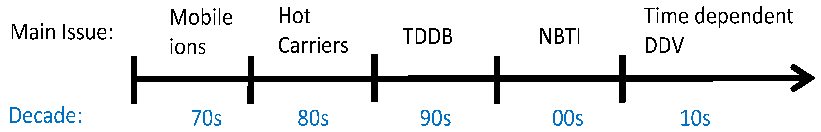
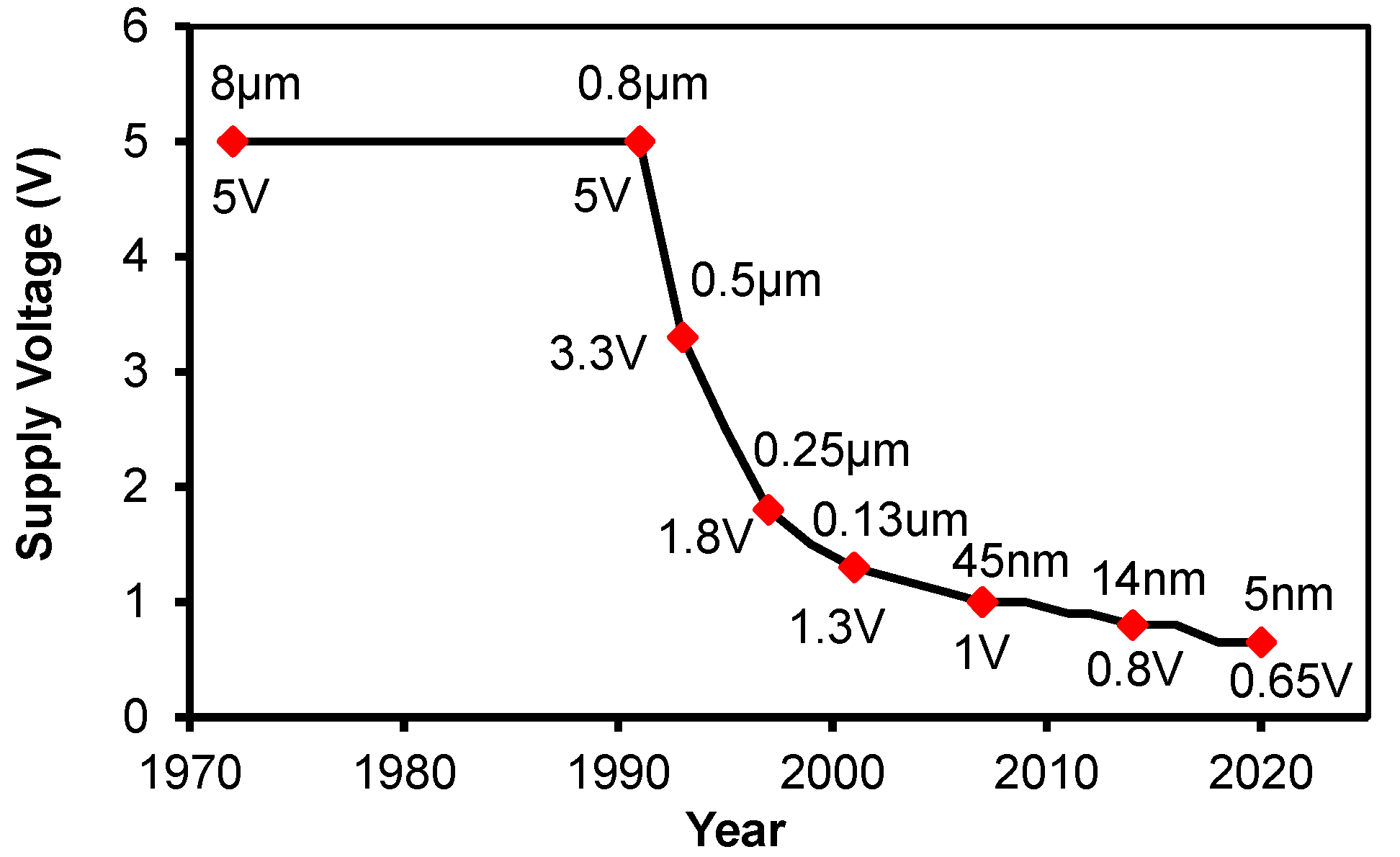
:1. Introduction
2. Negative Bias Temperature Instability (NBTI)
2.1. Pre-2000 NBTI
- Its recovery is insignificant;
- It also follows power law against gate bias;
- It is thermally activated.
2.2. Post-2000 NBTI
2.2.1. Difference from Pre-2000 NBTI
2.2.2. Failure of Early Models in Prediction
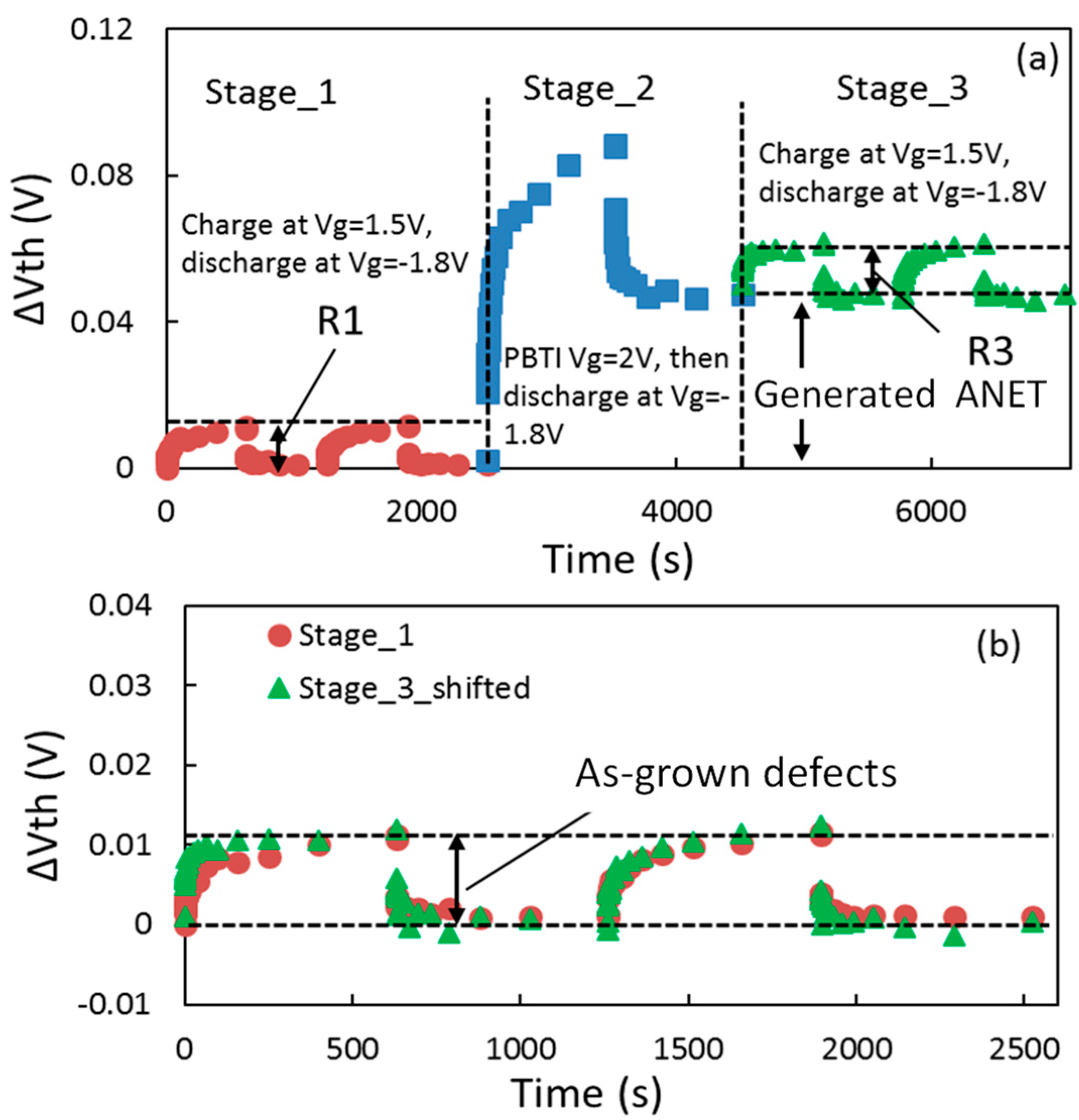
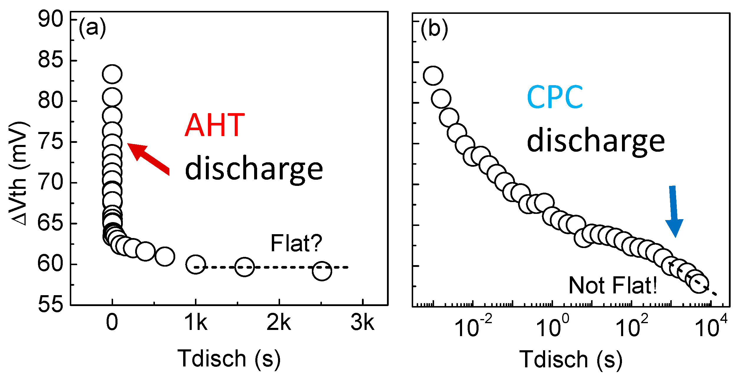
2.2.3. To Generate or Not to Generate, That Is the Question
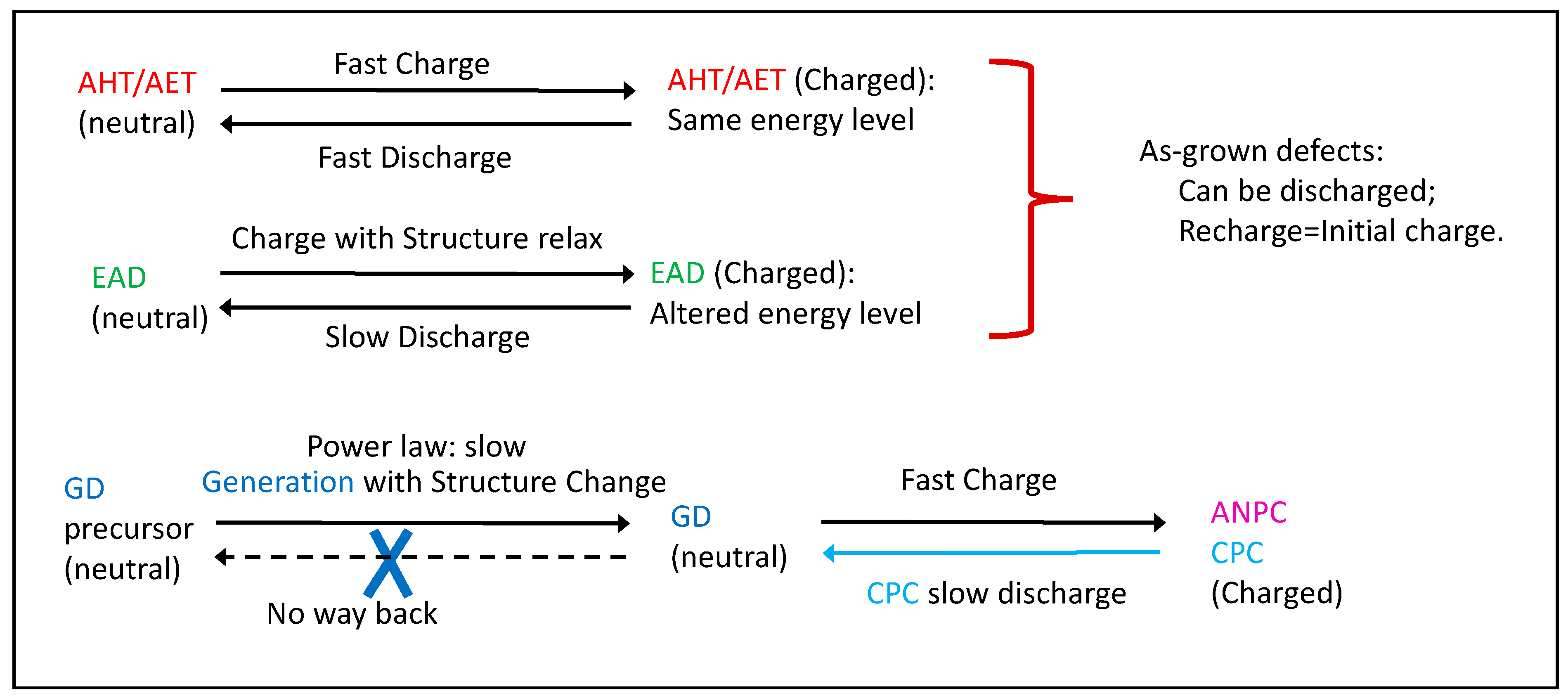
2.2.4. A New Modeling Approach: Separating As-Grown Traps from Generated Defects
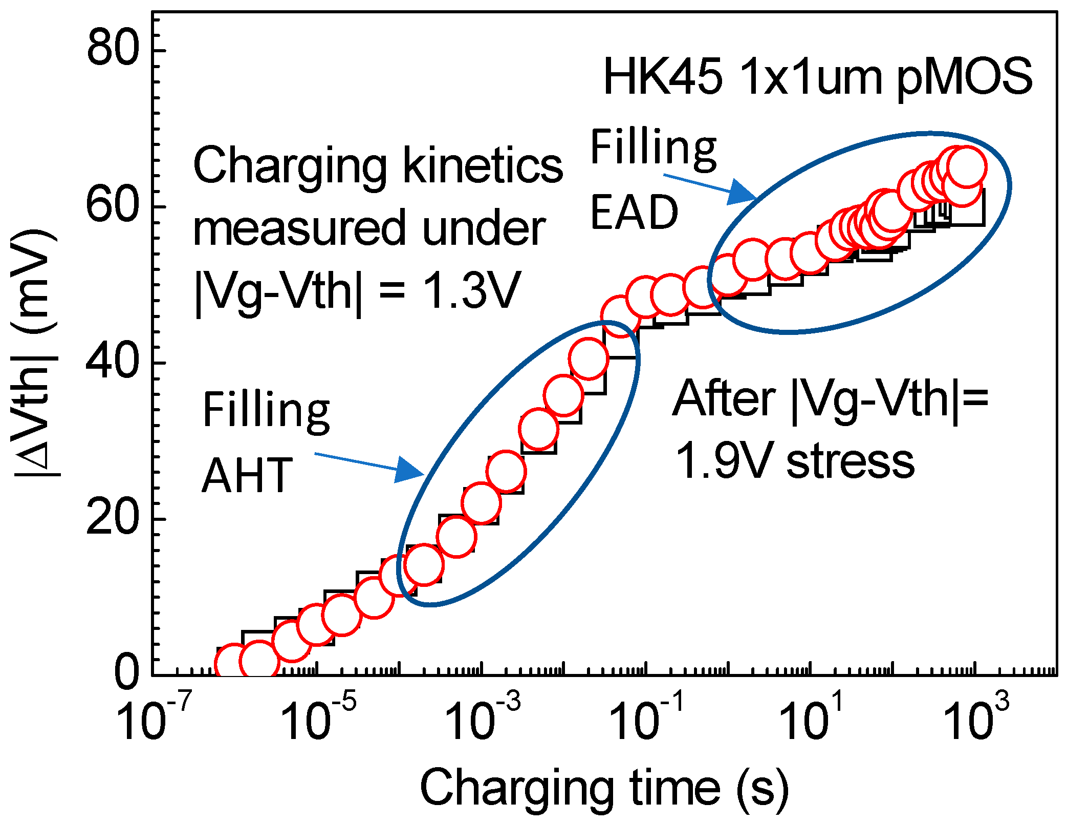
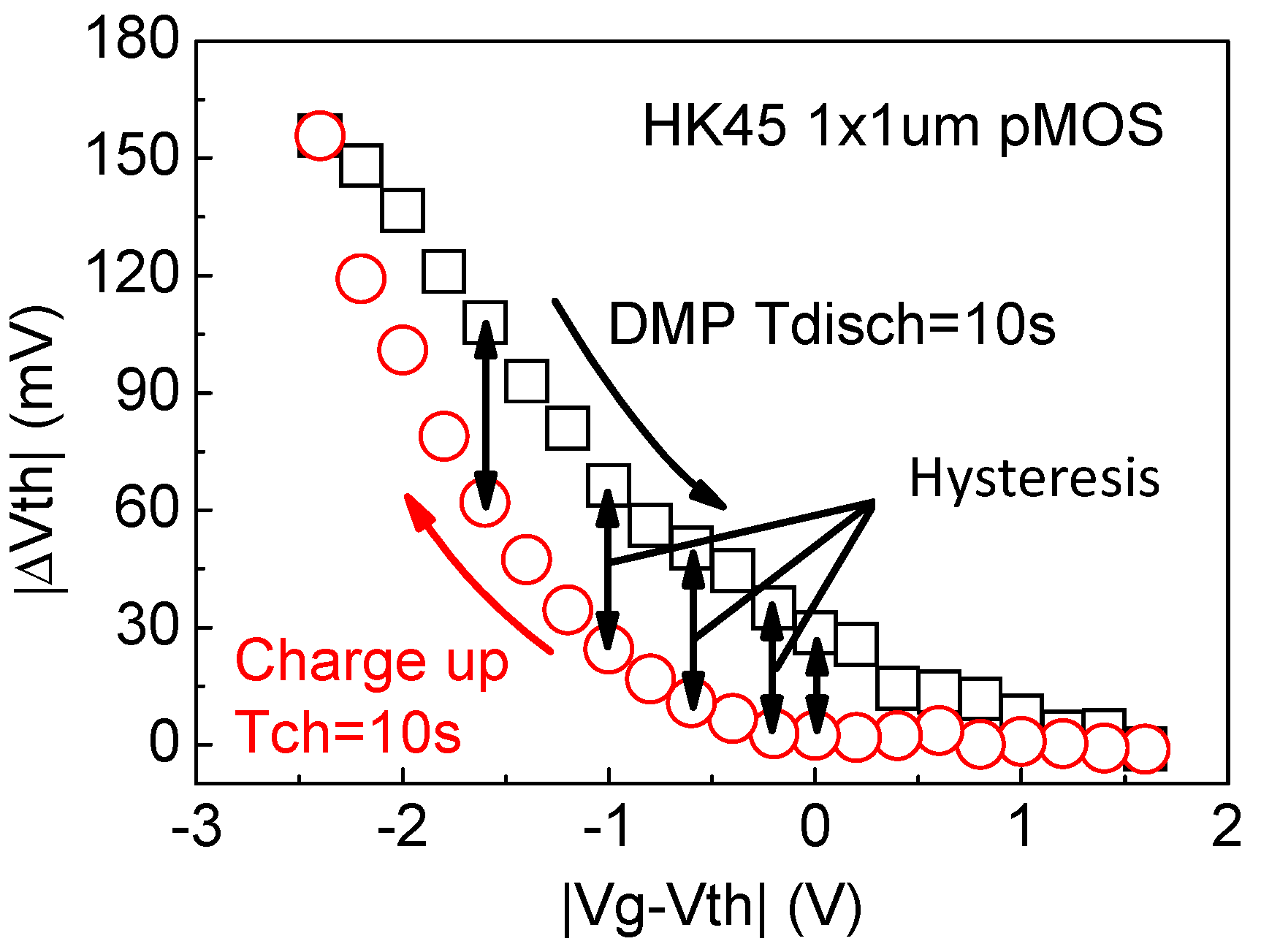
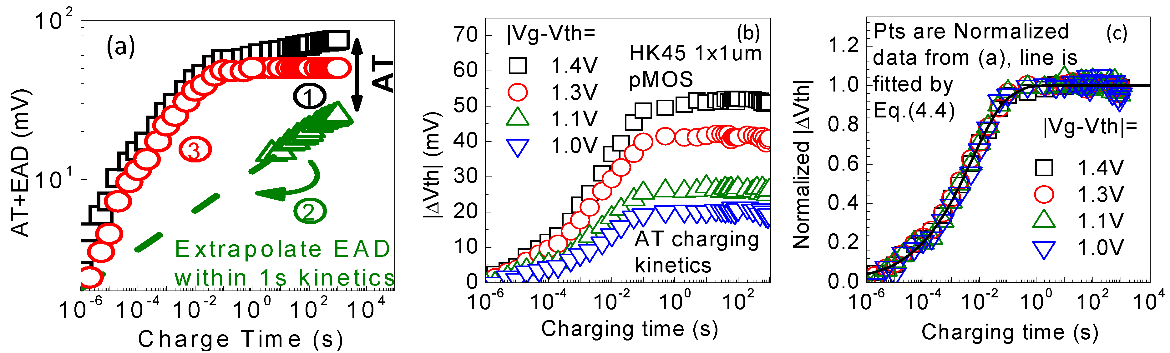
2.2.5. As-Grown Traps and Their Modeling
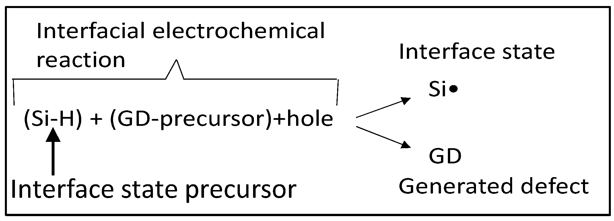
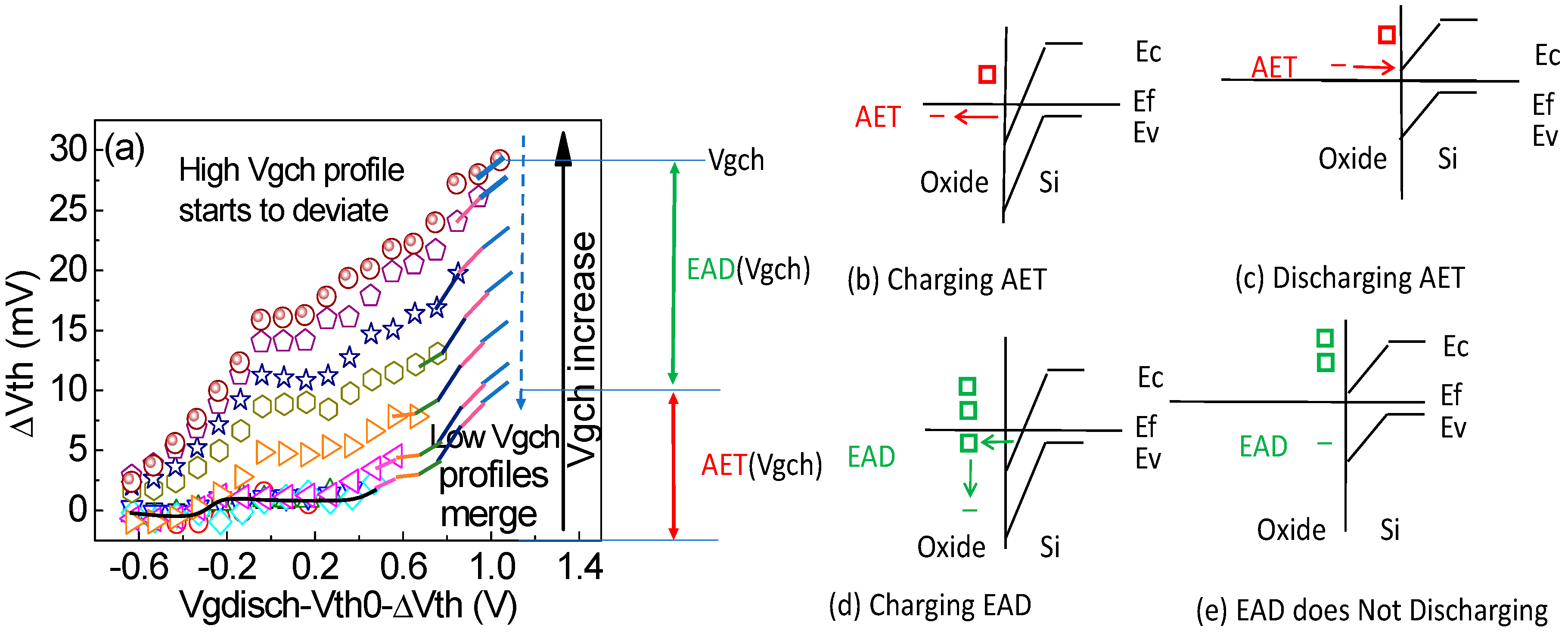
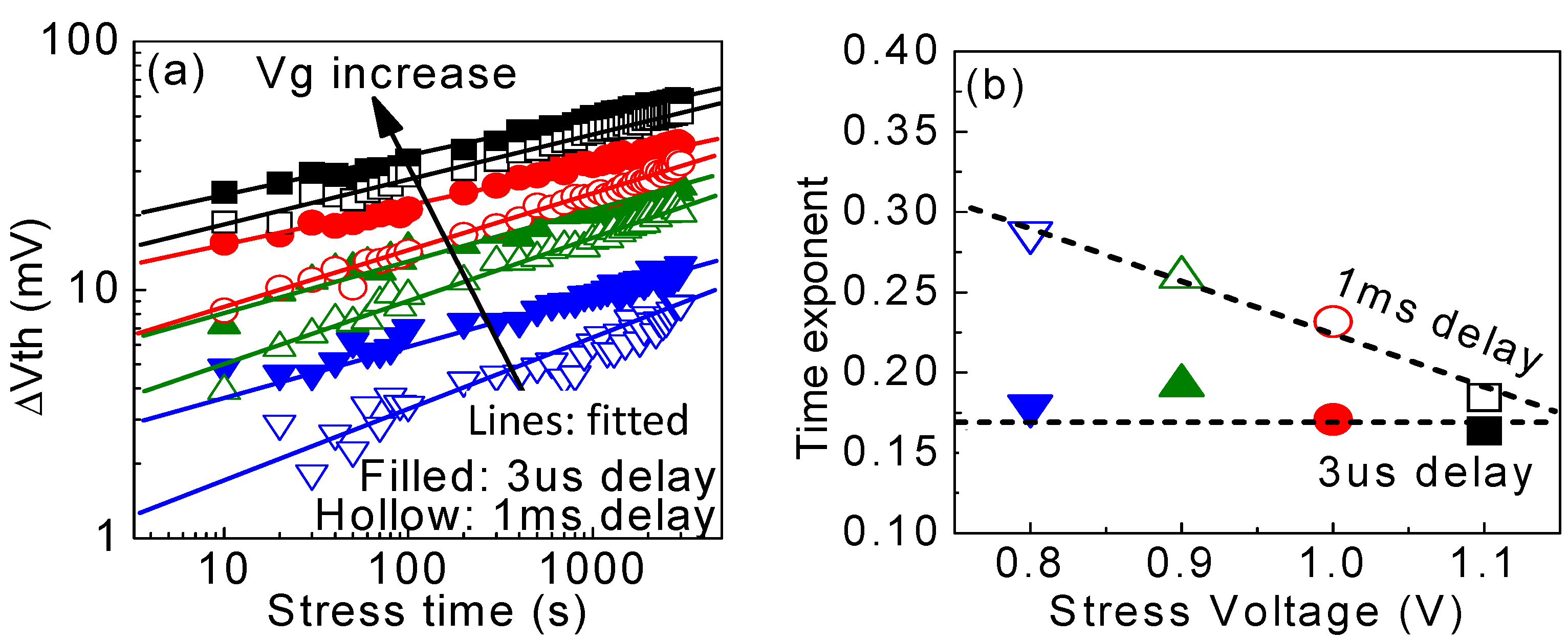
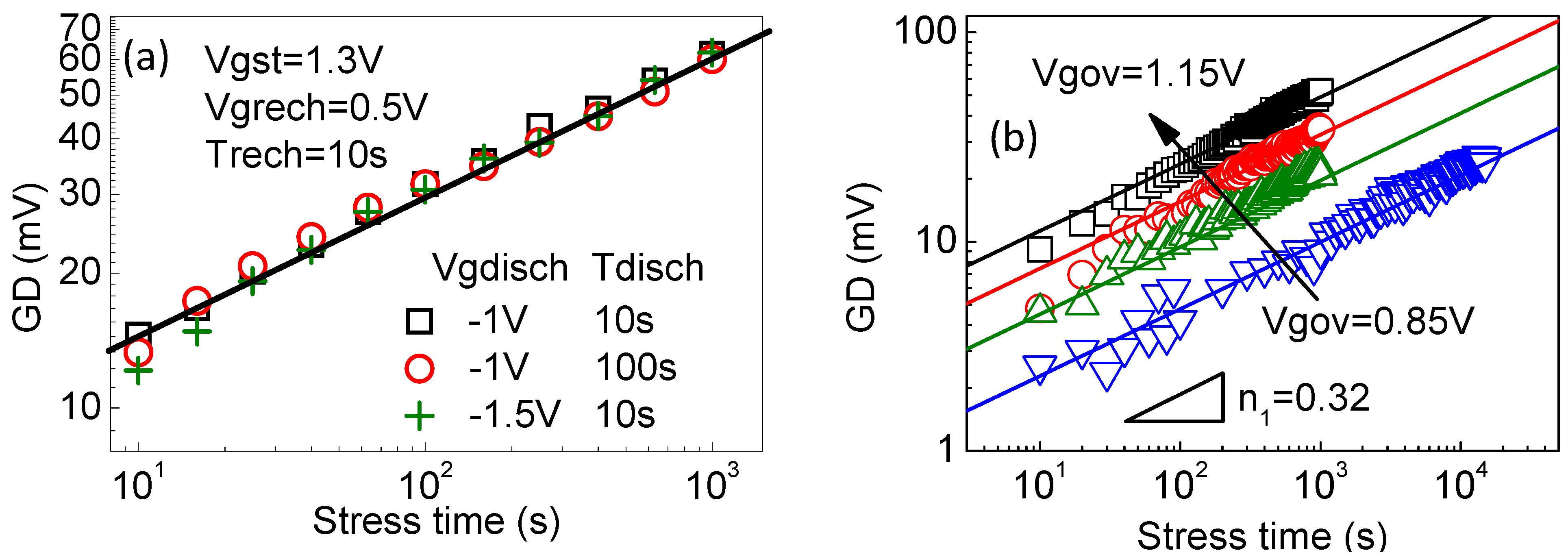
2.2.6. Two Types of Generated Traps
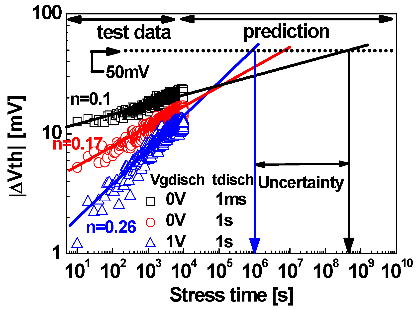
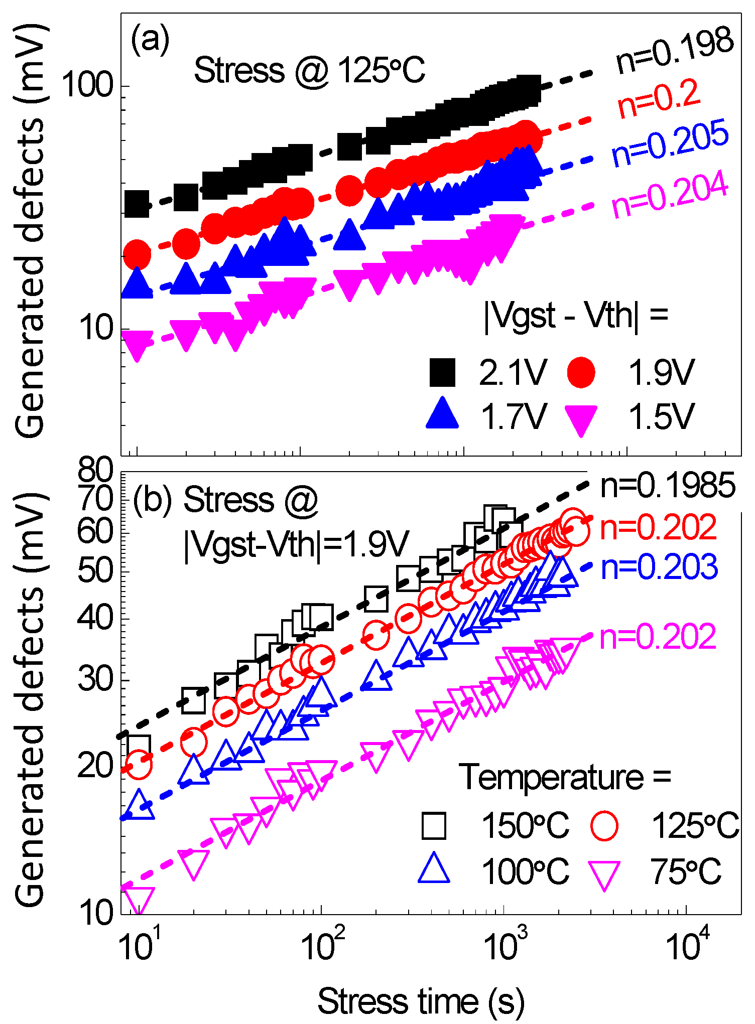
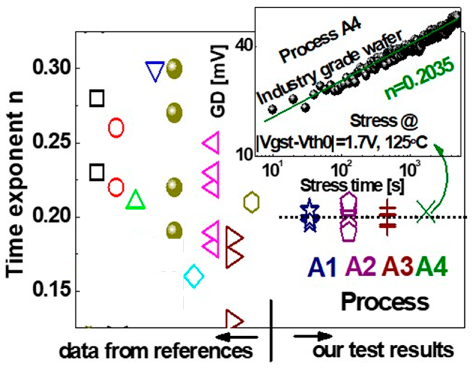
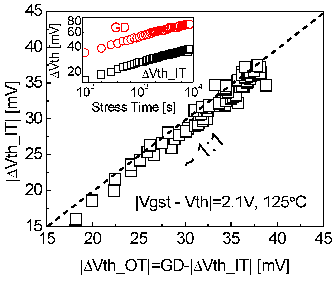
2.2.7. Modeling the Generated Traps
2.2.8. A Framework of Defects Responsible for NBTI
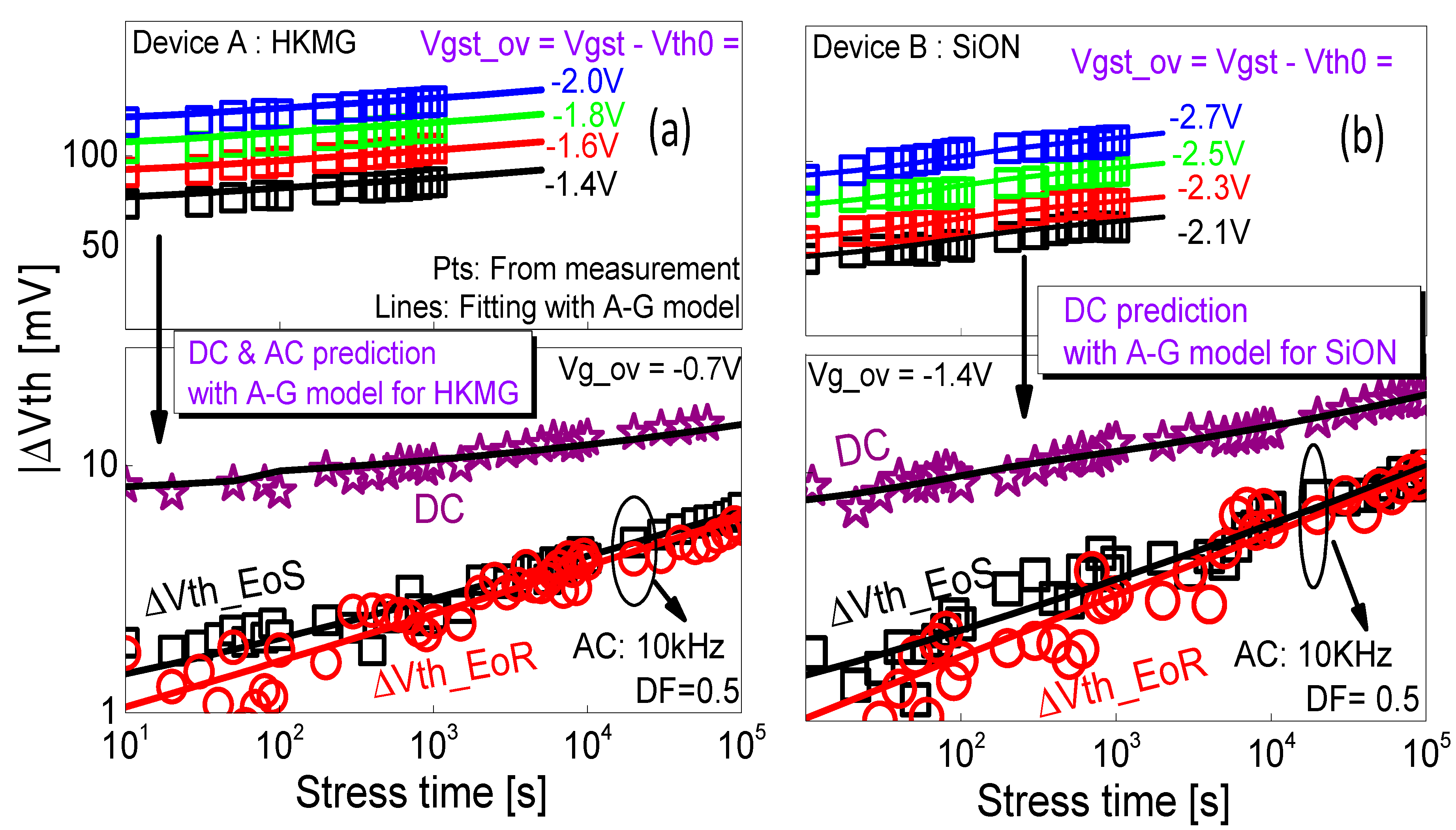
2.2.9. A Predictive As-Grown-Generation (AG) Model
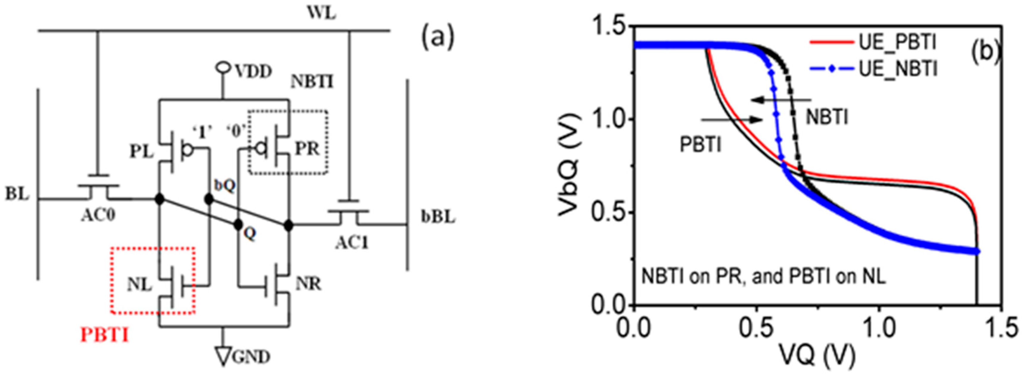
3. Positive Bias Temperature Instability (PBTI)
3.1. History of PBTI
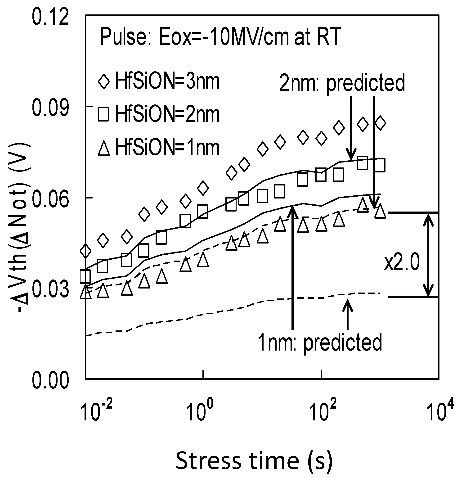
3.2. PBTI as the Limiting Instability during the Early Stage of High-k Process Development
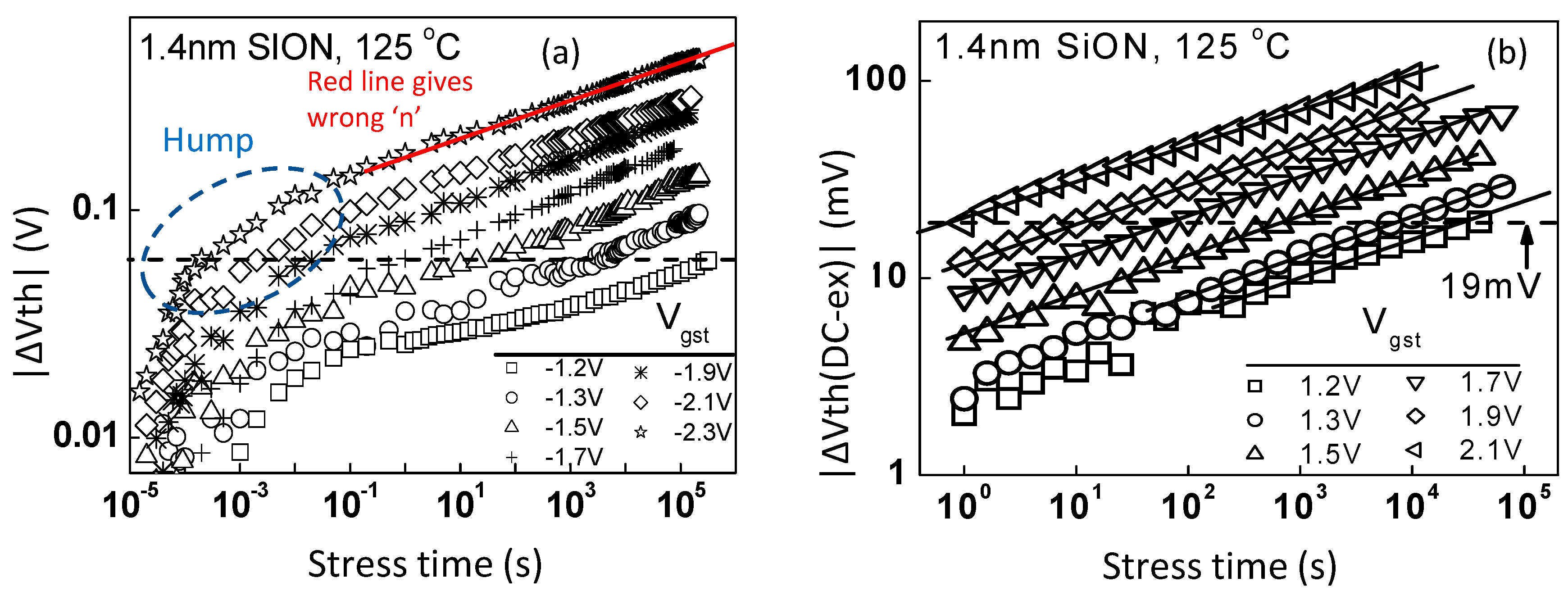
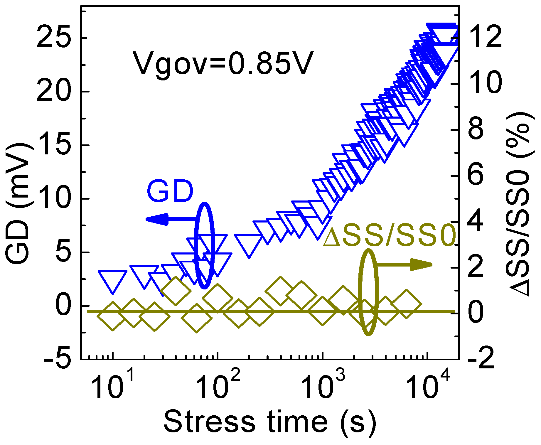
3.3. PBTI of Modern High-k/SiON Stacks
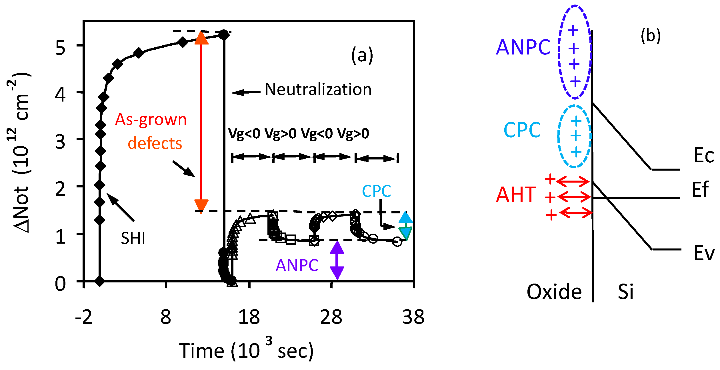
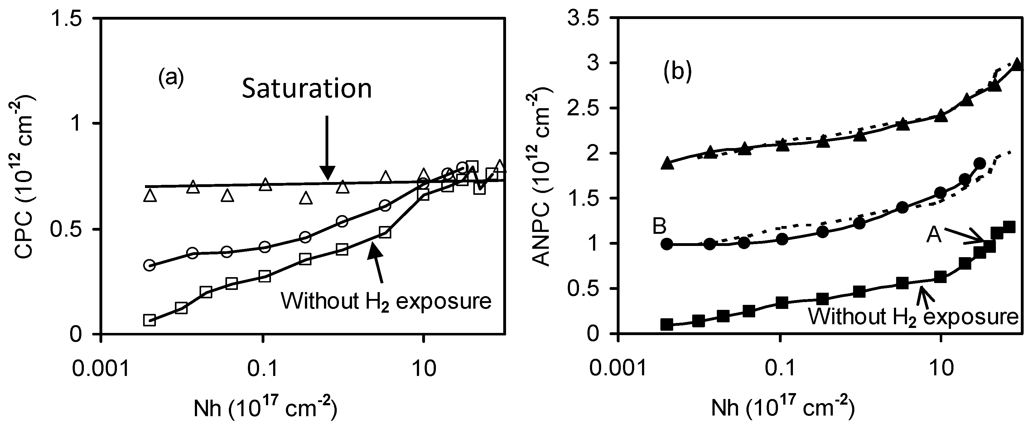
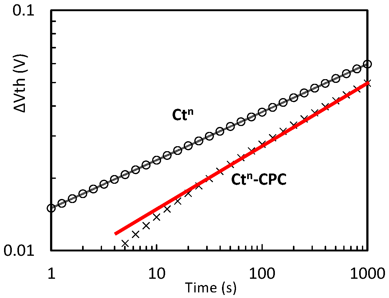
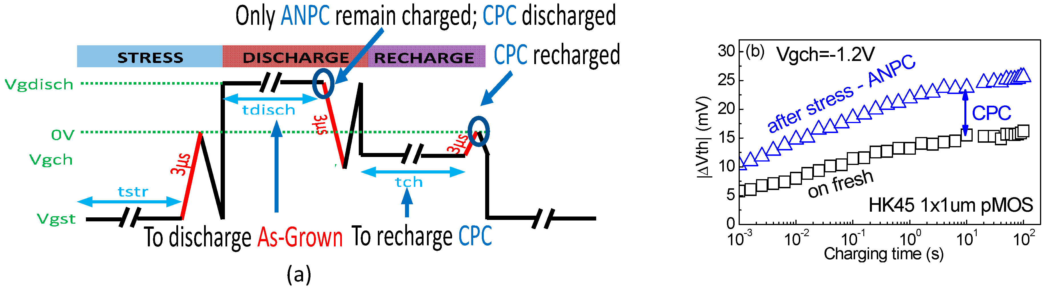
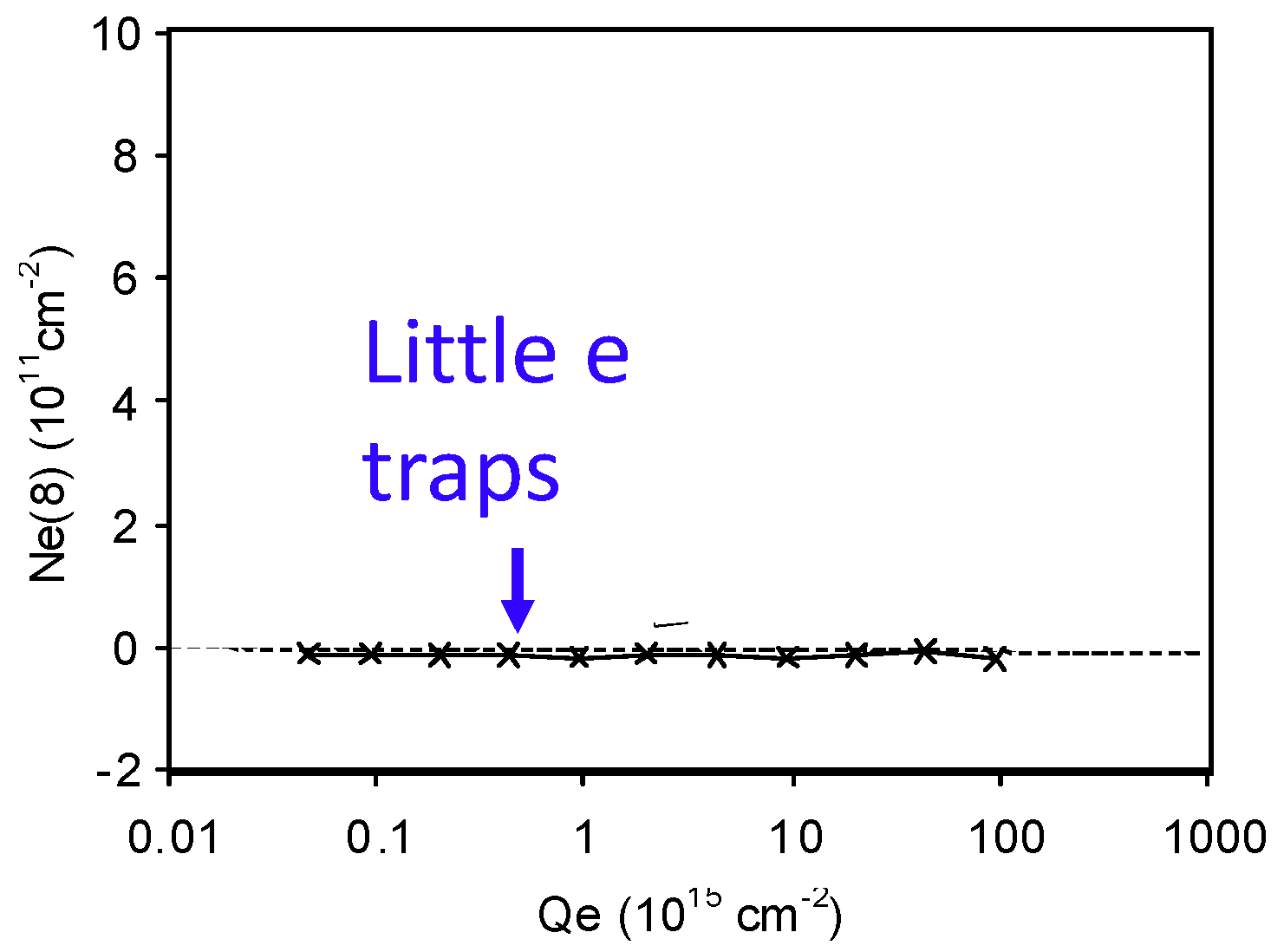
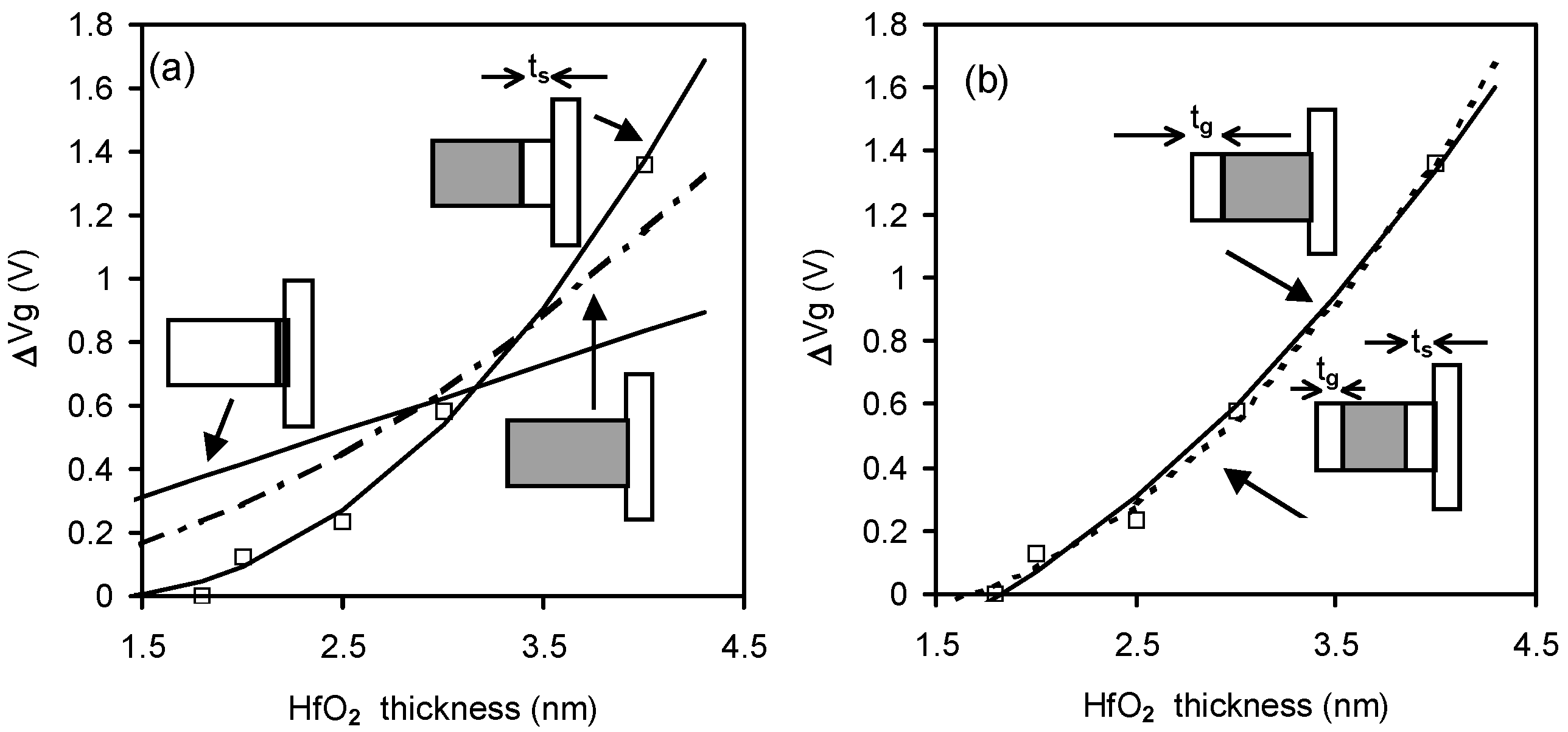
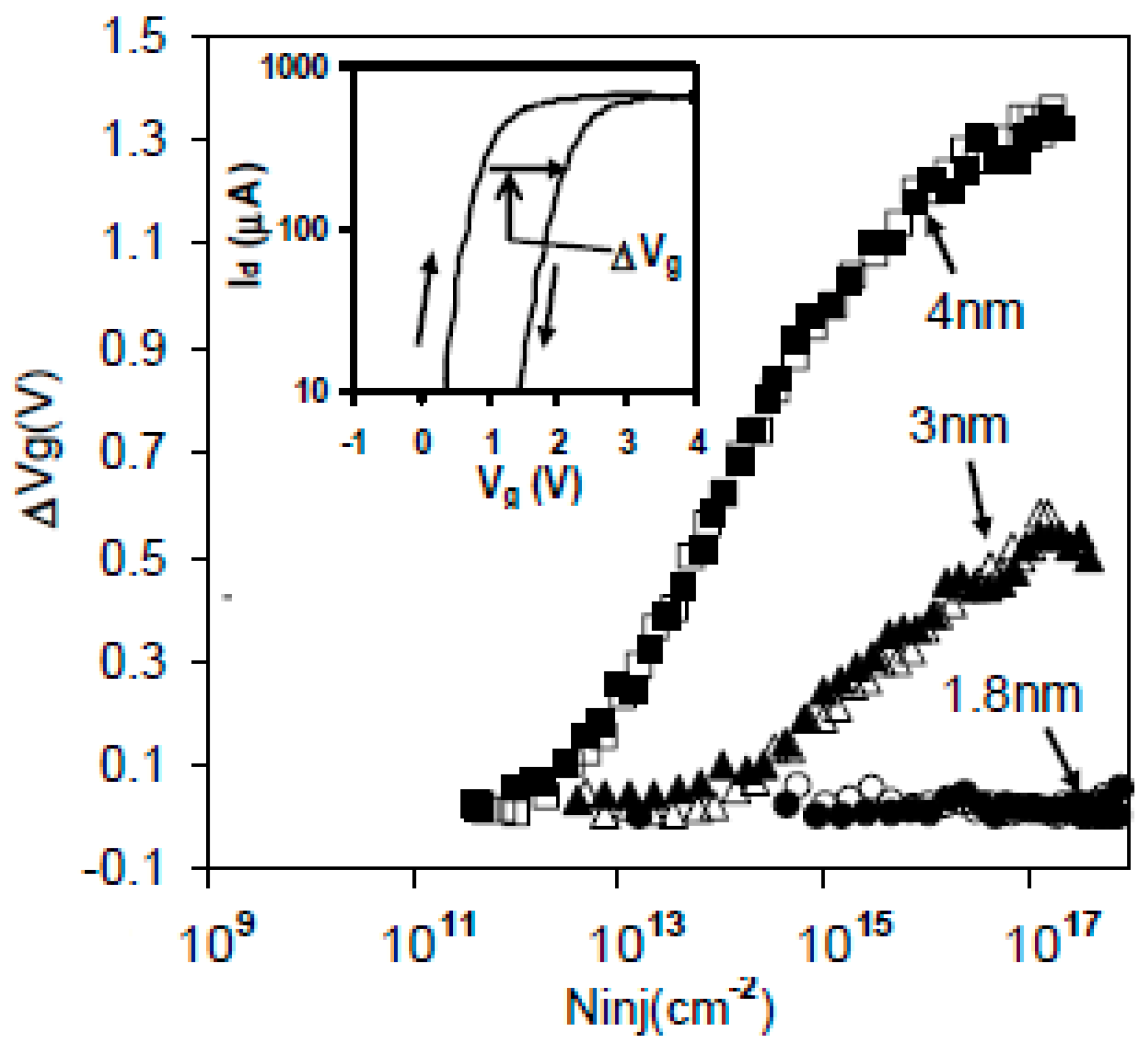
3.4. As-Grown Defects for PBTI
3.5. As-Grown-Generation (AG) Model of PBTI
4. Conclusions
Author Contributions
Funding
Acknowledgments
Conflicts of Interest
References
- Deal, B.E.; Sklar, M.; Grove, A.S.; Snow, E.H. Characteristics of the Surface-State Charge (Qss) of Thermally Oxidized Silicon. J. Electrochem. Soc. 1967, 114, 114–266. [Google Scholar] [CrossRef]
- Jepson, K.O.; Svensson, C.M. Negative bias stress of MOS devices at high electric fields and degradation of MNOS devices. J. Appl. Phys. 1977, 48, 2004–2014. [Google Scholar] [CrossRef] [Green Version]
- Blat, C.E.; Nicollian, E.H.; Poindexter, E.H. Mechanism of negative-bias-temperature instability. J. Appl. Phys. 1991, 69, 1712–1720. [Google Scholar] [CrossRef]
- Ogawa, S.; Shimaya, M.; Shiono, N. Interface-trap generation at ultrathin SiO2 (4–6 nm)-Si interfaces during negative-bias temperature aging. J. Appl. Phys. 1995, 77, 1137–1148. [Google Scholar] [CrossRef]
- Black, J.R. Electromigration Failure Modes in Aluminum Metallization for Semiconductor Devices. Proc. IEEE 1969, 57, 1587–1594. [Google Scholar] [CrossRef]
- Chen, F.; McLaughlin, P.; Gambino, J.; Wu, E.; Demarest, J.; Meatyard, D.; Shinosky, M. The Effect of Metal Area and Line Spacing on TDDB Characteristics of 45nm Low-k SiCOH Dielectrics. In Proceedings of the 2007 IEEE International Reliability Physics Symposium Proceedings, Phoenix, AZ, USA, 15–19 April 2007; pp. 382–389. [Google Scholar]
- Nauta, P.K.; Hillen, M.W. Investigation of mobile ions in MOS structures using the TSIC method. J. Appl. Phys. 1978, 49, 2862–2865. [Google Scholar] [CrossRef] [Green Version]
- Hu, C.; Tam, S.C.; Hsu, F.-C.; Ko, P.-K.; Chan, T.-Y.; Terrill, K.W. Hot-Electron-Induced MOSFET Degradation—Model, Monitor, and Improvement. IEEE J. Solid-State Circuits 1985, 20, 295–305. [Google Scholar] [CrossRef]
- Duan, M.; Zhang, J.F.; Manut, A.; Ji, Z.; Zhang, W.; Asenov, A.; Gerrer, L.; Reid, D.; Razaidi, H.; Vigar, D.; et al. Hot carrier aging and its variation under use-bias: Kinetics, prediction, impact on Vdd and SRAM. In Proceedings of the IEEE International Electron Devices Meeting (IEDM), Washington, DC, USA, 7–9 December 2015; pp. 547–550. [Google Scholar] [CrossRef] [Green Version]
- Degraeve, R.; Ogier, J.L.; Bellens, R.; Roussel, P.J.; Groeseneken, G.; Maes, H.E. A New Model for the Field Dependence of Intrinsic and Extrinsic Time-Dependent Dielectric Breakdown. IEEE Trans. Electron Devices 1998, 45, 472–481. [Google Scholar] [CrossRef]
- Kirton, M.J.; Uren, M.J. Noise in solid-state microstructures: A new perspective on individual defects, interface states and low-frequency (1/ƒ) noise. Adv. Phys. 1989, 38, 367–468. [Google Scholar] [CrossRef]
- Mehedi, M.; Tok, K.H.; Zhang, J.F.; Ji, Z.; Ye, Z.; Zhang, W.; Marsland, J.S. An assessment of the statistical distribution of Random Telegraph Noise Time Constants. IEEE Access 2020, 8, 1496–1499. [Google Scholar] [CrossRef]
- Mehedi, M.; Tok, K.H.; Ye, Z.; Zhang, J.F.; Ji, Z.; Zhang, W.; Marsland, J.S. On the Accuracy in Modeling the Statistical Distribution of Random Telegraph Noise Amplitude. IEEE Access 2021, 9, 43551–43561. [Google Scholar] [CrossRef]
- Tan, S.S.; Chen, T.P.; Ang, C.H.; Chan, L. Mechanism of nitrogen-enhanced negative bias temperature instability in pMOSFET. Microelectron. Reliab. 2005, 45, 19–30. [Google Scholar] [CrossRef]
- Kaczer, B.; Grasser, T.; Roussel, P.J.; Franco, J.; Degraeve, R.; Ragnarsson, L.-A.; Simoen, E.; Groeseneken, G.; Reisinger, H. Origin of NBTI variability in deeply scaled pFETs. In Proceedings of the 2010 IEEE International Reliability Physics Symposium, Anaheim, CA, USA, 2–6 May 2010; pp. 26–32. [Google Scholar] [CrossRef]
- Grasser, T. Stochastic charge trapping in oxides: From random telegraph noise to bias temperature instabilities. Microelectron. Rel. 2012, 52, 39–70. [Google Scholar] [CrossRef]
- Zhang, J.F.; Ji, Z.; Zhang, W. As-grown-generation (AG) model of NBTI: A shift from fitting test data to prediction. Microelectron. Rel. 2018, 80, 109–123. [Google Scholar] [CrossRef] [Green Version]
- Waldhoer, D.; Schleich, C.; Michl, J.; Stampfer, B.; Tselios, K.; Ioannidis, E.G.; Enichlmair, H.; Waltl, M.; Grasser, T. Toward Automated Defect Extraction From Bias Temperature Instability Measurements. IEEE Trans. Electron Devices 2021, 68, 4057–4063. [Google Scholar] [CrossRef]
- Zhang, J.; Wang, Z.; Wang, R.; Sun, Z.; Huang, R. Body Bias Dependence of Bias Temperature Instability(BTI) in Bulk FinFET Technology. Energy Environ. Mater. 2021, 1–4. [Google Scholar] [CrossRef]
- Lee, J. Physics-informed machine learning model for bias temperature instability. AIP Adv. 2021, 11, 025111. [Google Scholar] [CrossRef]
- Kishida, R.; Suda, I.; Kobayashi, K. Bias Temperature Instability Depending on Body Bias through Buried Oxide (BOX) Layer in a 65 nm Fully-Depleted Silicon-On-Insulator Process. In Proceedings of the 2021 IEEE International Reliability Physics Symposium (IRPS), Monterey, CA, USA, 21–25 March 2021. [Google Scholar] [CrossRef]
- Bhootda, N.; Yadav, A.; Neema, V.; Shah, A.P.; Vishvakarma, S.K. Series diode-connected current mirror based linear andsensitive negative bias temperature instability monitoringcircuit. Int. J. Numer. Model. 2022, 35, e2953. [Google Scholar] [CrossRef]
- Hicks, J.; Bergstrom, D.; Hattendorf, M.; Jopling, J.; Maiz, J.; Pae, S.; Prasad, C.; Wiedemer, J. 45 nm Transistor Reliability. Intel Technol. J. 2008, 12, 131–144. [Google Scholar] [CrossRef]
- Zhao, C.Z.; Zahid, M.B.; Zhang, J.F.; Groeseneken, G.; Degraeve, R.; De Gendt, S. Properties and dynamic behavior of electron traps in HfO2/SiO2 stacks. Microelectron. Eng. 2005, 80, 366–369. [Google Scholar] [CrossRef]
- Zhao, C.Z.; Zhang, J.F.; Zahid, M.B.; Govoreanu, B.; Groeseneken, G.; De Gendt, S. Determination of capture cross sections for as-grown electron traps in HfO2/HfSiO stacks. J. Appl. Phys. 2006, 100, 093716. [Google Scholar] [CrossRef]
- Asenov, A.; Cheng, B.; Dideban, D.; Kovac, U.; Moezi, N.; Millar, C.; Roy, G.; Brown, A.R.; Roy, S. Modeling and simulation of transistor and circuit variability and reliability. In Proceedings of the IEEE Custom Integrated Circuits Conference 2010, San Jose, CA, USA, 19–22 September 2010; pp. 1–8. [Google Scholar] [CrossRef]
- Duan, M.; Zhang, J.F.; Ji, Z.; Zhang, W.; Kaczer, B.; Schram, T.; Ritzenthaler, R.; Groeseneken, G.; Asenov, A. New analysis method for time-dependent device-to-device variation accounting for within-device fluctuation. IEEE Trans. Electron Devices 2013, 60, 2505–2511. [Google Scholar] [CrossRef]
- Duan, M.; Zhang, J.F.; Ji, Z.; Ma, J.G.; Zhang, W.; Kaczer, B.; Schram, T.; Ritzenthaler, R.; Groeseneken, G.; Asenov, A. Key issues and Techniques for Characterizing Time-Dependent Device-to-Device Variation of SRAM. In Proceedings of the 2013 IEEE International Electron Devices Meeting, Washington, DC, USA, 9–11 December 2013; pp. 774–777. [Google Scholar] [CrossRef]
- Duan, M.; Zhang, J.F.; Ji, Z.; Zhang, W.; Kaczer, B.; Schram, T.; Ritzenthaler, R.; Groeseneken, G.; Asenov, A. Development of a Technique for Characterizing Bias Temperature Instability-Induced Device-to-Device Variation at SRAM-Relevant Conditions. IEEE Trans. Electron Devices 2014, 61, 3081–3089. [Google Scholar] [CrossRef]
- Duan, M.; Zhang, J.F.; Ji, Z.; Zhang, W.; Kaczer, B.; Schram, T.; Ritzenthaler, R.; Thean, A.; Groeseneken, G.; Asenov, A. Time-dependent variation: A new defect-based prediction methodology. In Proceedings of the 014 Symposium on VLSI Technology (VLSI-Technology): Digest of Technical Papers, Honolulu, HI, USA, 9–12 June 2014; pp. 74–75. [Google Scholar] [CrossRef]
- Gao, R.; Ji, Z.; Manut, A.B.; Zhang, J.F.; Franco, J.; Hatta, S.W.M.; Zhang, W.; Kaczer, B.; Linten, D.; Groeseneken, G. NBTI-Generated Defects in Nanoscaled Devices: Fast Characterization Methodology and Modeling. IEEE Trans. Electron Devices 2017, 64, 4011–4017. [Google Scholar] [CrossRef]
- Mahapatra, S.; Goel, N.; Desai, S.; Gupta, S.; Jose, B.; Mukhopadhyay, S.; Joshi, K.; Jain, A.; Islam, A.E.; Alam, M.A. A Comparative Study of Different Physics-Based NBTI Models. IEEE Trans. Electron Devices 2013, 60, 901–916. [Google Scholar] [CrossRef]
- Huard, V. Two independent components modeling for Negative Bias Temperature Instability. In Proceedings of the 2010 IEEE International Reliability Physics Symposium, Anaheim, CA, USA, 2–6 May 2010; pp. 33–42. [Google Scholar] [CrossRef]
- Huard, V.; Parthasarathy, C.R.; Bravaix, A.; Hugel, T.; Guerin, C.; Vincent, E. Design-in-Reliability Approach for NBTI and Hot-Carrier Degradations in Advanced Nodes. IEEE Trans. Device Mater. Reliab. 2007, 7, 558–570. [Google Scholar] [CrossRef]
- Ji, Z.; Hatta, S.F.W.M.; Zhang, J.F.; Ma, J.G.; Zhang, W.; Soin, N.; Kaczer, B.; De Gendt, S.; Groeseneken, G. Negative Bias Temperature Instability Lifetime Prediction: Problems and Solutions. In Proceedings of the 2013 IEEE International Electron Devices Meeting, Washington, DC, USA, 9–11 December 2013; pp. 413–416. [Google Scholar] [CrossRef]
- Ji, Z.; Zhang, J.F.; Lin, L.; Duan, M.; Zhang, W.; Zhang, X.; Gao, R.; Kaczer, B.; Franco, J.; Schram, T.; et al. A test-proven As-grown-Generation (A-G) model for predicting NBTI under use-bias. In Proceedings of the 2015 Symposium on VLSI Technology (VLSI Technology), Kyoto, Japan, 16–18 June 2015; pp. 36–37. [Google Scholar] [CrossRef] [Green Version]
- Gao, R.; Ji, Z.; Hatta, S.M.; Zhang, J.F.; Franco, J.; Kaczer, B.; Zhang, W.; Duan, M.; De Gendt, S.; Linten, D.; et al. Predictive As-grown-Generation (A-G) model for BTI-induced device/circuit level variations in nanoscale technology nodes. In Proceedings of the 2016 IEEE International Electron Devices Meeting (IEDM), San Francisco, CA, USA, 3–7 December 2016; pp. 778–781. [Google Scholar] [CrossRef]
- Gao, R.; Manut, A.B.; Ji, Z.; Ma, J.; Duan, M.; Zhang, J.F.; Franco, J.; Hatta, S.W.M.; Zhang, W.; Kaczer, B.; et al. Reliable time exponents for long term prediction of negative bias temperature instability by extrapolation. IEEE Trans. Electron Devices 2017, 64, 1467–1473. [Google Scholar] [CrossRef]
- Gao, R.; Ji, Z.; Zhang, J.F.; Marsland, J.; Zhang, W.D. As-grown-Generation Model for Positive Bias Temperature Instability. IEEE Trans. Electron Devices 2018, 65, 3662–3668. [Google Scholar] [CrossRef]
- Aiello, O.; Fiori, F. On the Susceptibility of Embedded Thermal Shutdown Circuit to Radio Frequency Interference. IEEE Trans. Electromagn. Compat. 2012, 54, 405–412. [Google Scholar] [CrossRef]
- Xie, S. The Design Considerations and Challenges in MOS-Based Temperature Sensors: A Review. Electronics 2022, 11, 1019. [Google Scholar] [CrossRef]
- Kim, J.; Koo, Y.; Song, W.; Hong, S.J. On-Wafer Temperature Monitoring Sensor for Condition Monitoring of Repaired Electrostatic Chuck. Electronics 2022, 11, 880. [Google Scholar] [CrossRef]
- Zhang, J.F.; Chang, M.H.; Ji, Z.; Lin, L.; Ferain, I.; Groeseneken, G.; Pantisano, L.; De Gendt, S.; Heyns, M.M. Dominant layer for stress-induced positive charges in Hf-based gate stacks. IEEE Electron Device Lett. 2008, 29, 360–1363. [Google Scholar] [CrossRef]
- Chang, M.H.; Zhang, J.F. On positive charges formed under negative bias temperature stresses. J. Appl. Phys. 2007, 101, 024516. [Google Scholar] [CrossRef]
- Ji, Z.; Zhang, J.F.; Chang, M.H.; Kaczer, B.; Groeseneken, G. An analysis of the NBTI-induced threshold voltage shift evaluated by different techniques. IEEE Trans. Electron Devices 2009, 56, 1086–1093. [Google Scholar] [CrossRef]
- Ji, Z.; Lin, L.; Zhang, J.F.; Kaczer, B.; Groeseneken, G. NBTI lifetime prediction and kinetics at operation bias based on ultrafast pulse measurement. IEEE Trans. Electron Devices 2010, 57, 228–237. [Google Scholar] [CrossRef]
- Duan, M.; Zhang, J.F.; Ji, Z.; Zhang, W.; Kaczer, B.; De Gendt, S.; Groeseneken, G. Defect loss: A new concept for reliability of MOSFETs. IEEE Electron Device Lett. 2012, 33, 480–482. [Google Scholar] [CrossRef]
- Zhang, J.F.; Sii, H.K.; Groeseneken, G.; Degraeve, R. Hole trapping and trap generation in the gate silicon dioxide. IEEE Trans. Electron Devices 2001, 48, 1127–1135. [Google Scholar] [CrossRef]
- Zhang, J.F.; Zhao, C.Z.; Chen, A.H.; Groeseneken, G.; Degraeve, R. Hole traps in silicon dioxides—Part I: Properties. IEEE Trans. Electron Devices 2004, 51, 1267–1273. [Google Scholar] [CrossRef]
- Zhao, C.Z.; Zhang, J.F.; Groeseneken, G.; Degraeve, R. Hole traps in silicon dioxides—Part II: Generation mechanism. IEEE Trans. Electron Devices 2004, 51, 1274–1280. [Google Scholar] [CrossRef]
- Zhao, C.Z.; Zhang, J.F.; Chang, M.H.; Peaker, A.R.; Hall, S.; Groeseneken, G.; Pantisano, L.; De Gendt, S.; Heyns, M.M. Stress-induced positive charge in Hf-based gate dielectrics: Impact on device performance and a framework for the defect. IEEE Trans. Electron Devices 2008, 55, 1647–1656. [Google Scholar] [CrossRef]
- Zhang, W.D.; Zhang, J.F.; Zhao, C.Z.; Chang, M.H.; Groeseneken, G.; Degraeve, R. Electrical signature of the defect associated with gate oxide breakdown. IEEE Electron Device Lett. 2006, 27, 393–395. [Google Scholar] [CrossRef]
- Gao, R. Bias Temperature Instability Modelling and Lifetime Prediction on Nano-Scale MOSFETs. Ph.D. Thesis, Liverpool John Moores University, Merseyside, UK, 2018. [Google Scholar]
- Zhao, C.Z.; Zhang, J.F. Effects of hydrogen on positive charges in gate oxides. J. Appl. Phys. 2005, 97, 073703. [Google Scholar] [CrossRef]
- Duan, M.; Zhang, J.F.; Ji, Z.; Zhang, W.; Vigar, D.; Asenov, A.; Gerrer, L.; Chandra, V.; Aitken, R.; Kaczer, B. Insight into Electron Traps and Their Energy Distribution under Positive Bias Temperature Stress and Hot Carrier Aging. IEEE Trans. Electron Devices 2016, 63, 3642–3648. [Google Scholar] [CrossRef]
- DeKeersmaecker, R.F.; DiMaria, D.J. Electron trapping and detrapping characteristics of arsenic-implanted SiO2 layers. J. Appl. Phys. 1980, 51, 1085–1101. [Google Scholar] [CrossRef]
- Nicollian, E.H.; Berglund, C.N.; Schmidt, P.F.; Andrews, J.M. Electrochemical Charging of Thermal SiO2 Films by Injected Electron Currents. J. Appl. Phys. 1971, 42, 5654–5664. [Google Scholar] [CrossRef]
- Zhang, J.F. Oxide defects. In Bias Temperature Instabilities for Devices and Circuits; Springer: Berlin/Heidelberg, Germany, 2014; pp. 253–285. [Google Scholar] [CrossRef]
- Zhang, J.F.; Taylor, S.; Eccleston, W. Electron Trap Generation in Thermally Grown Silicon Dioxide Under Fowler-Nordheim Stress. J. Appl. Phys. 1992, 71, 725–734. [Google Scholar] [CrossRef]
- Zhang, J.F.; Taylor, S.; Eccleston, W. A Quantitative Investigation of Electron Detrapping in SiO2 Under Fowler-Nordheim Stress. J. Appl. Phys. 1992, 71, 5989–5996. [Google Scholar] [CrossRef]
- Zhang, J.F.; Taylor, S.; Eccleston, W. A Comparative Study of The Electron Trapping and Thermal Detrapping in SiO2 Prepared by Plasma and Thermal Oxidation. J. Appl. Phys. 1992, 72, 1429–1435. [Google Scholar] [CrossRef]
- Zhang, W.D.; Zhang, J.F.; Lalor, M.; Burton, D.; Groeseneken, G.; Degraeve, R. Two types of neutral electron traps generated in the gate silicon dioxide. IEEE Trans. Electron Devices 2002, 49, 1868–1875. [Google Scholar] [CrossRef]
- Zhang, J.F.; Zhao, C.Z.; Zahid, M.B.; Groeseneken, G.; Degraeve, R.; De Gendt, S. An assessment of the location of as-grown electron traps in HfO2/HiSiO stacks. IEEE Electron Device Lett. 2006, 27, 817–820. [Google Scholar] [CrossRef]


| Defects | Formula |
|---|---|
| Saturation level of AHT/AET | |
| Filling AHT/AET | |
| EAD | |
| GD |
Publisher’s Note: MDPI stays neutral with regard to jurisdictional claims in published maps and institutional affiliations. |
© 2022 by the authors. Licensee MDPI, Basel, Switzerland. This article is an open access article distributed under the terms and conditions of the Creative Commons Attribution (CC BY) license (https://creativecommons.org/licenses/by/4.0/).
Share and Cite
Zhang, J.F.; Gao, R.; Duan, M.; Ji, Z.; Zhang, W.; Marsland, J. Bias Temperature Instability of MOSFETs: Physical Processes, Models, and Prediction. Electronics 2022, 11, 1420. https://doi.org/10.3390/electronics11091420
Zhang JF, Gao R, Duan M, Ji Z, Zhang W, Marsland J. Bias Temperature Instability of MOSFETs: Physical Processes, Models, and Prediction. Electronics. 2022; 11(9):1420. https://doi.org/10.3390/electronics11091420
Chicago/Turabian StyleZhang, Jian Fu, Rui Gao, Meng Duan, Zhigang Ji, Weidong Zhang, and John Marsland. 2022. "Bias Temperature Instability of MOSFETs: Physical Processes, Models, and Prediction" Electronics 11, no. 9: 1420. https://doi.org/10.3390/electronics11091420
APA StyleZhang, J. F., Gao, R., Duan, M., Ji, Z., Zhang, W., & Marsland, J. (2022). Bias Temperature Instability of MOSFETs: Physical Processes, Models, and Prediction. Electronics, 11(9), 1420. https://doi.org/10.3390/electronics11091420