
Resonance-Enhanced Quantum Well Micropillar Array with Ultra-Narrow Bandwidth and Ultra-High Peak Quantum Efficiency

Abstract
:1. Introduction
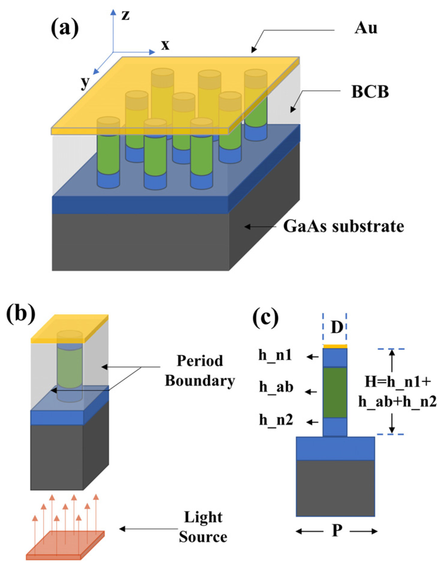
2. Physical Model
3. Results
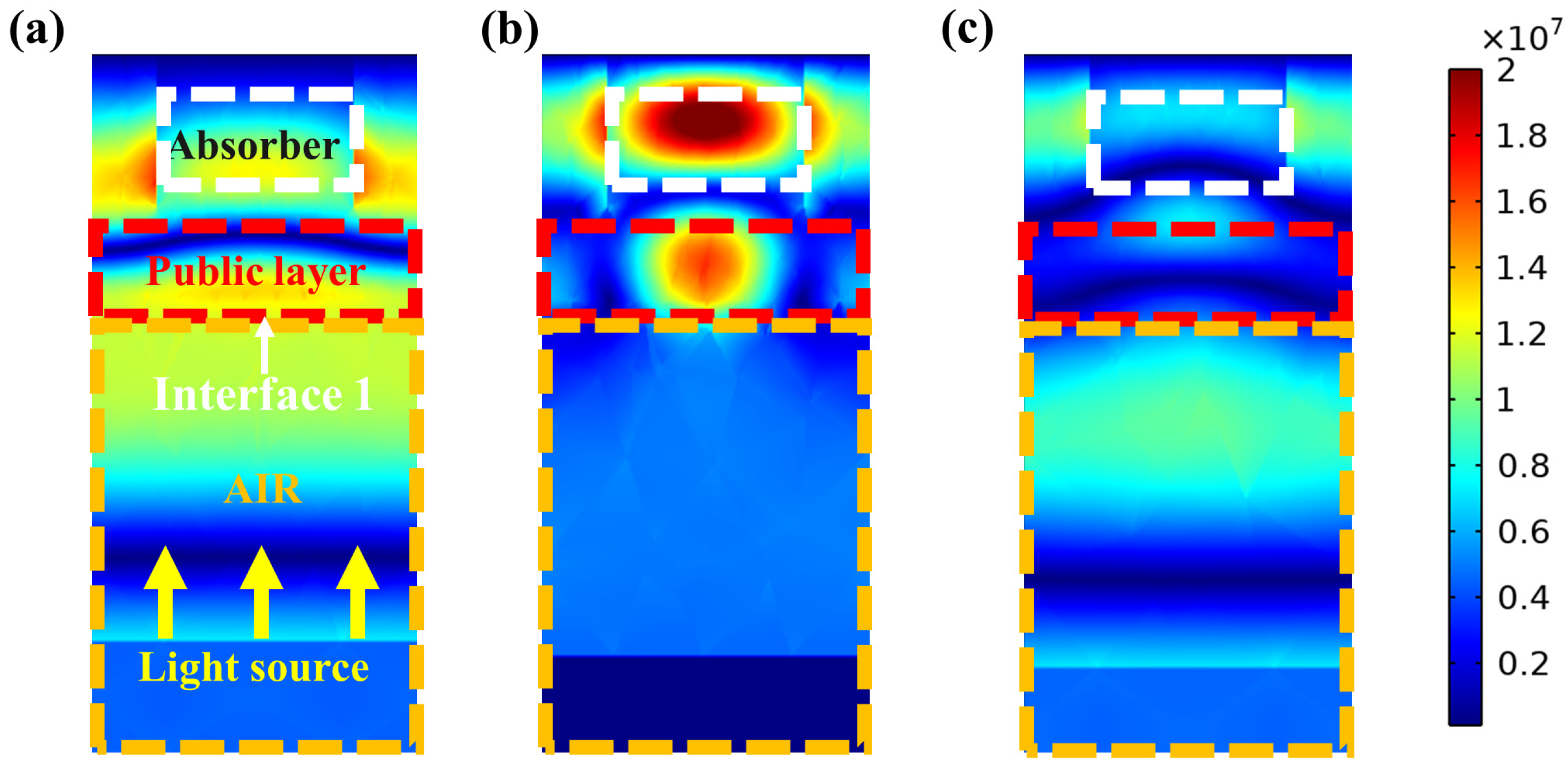
3.1. Operating Mechanism of Quantum Well Micropillar Array under the Back Incidence
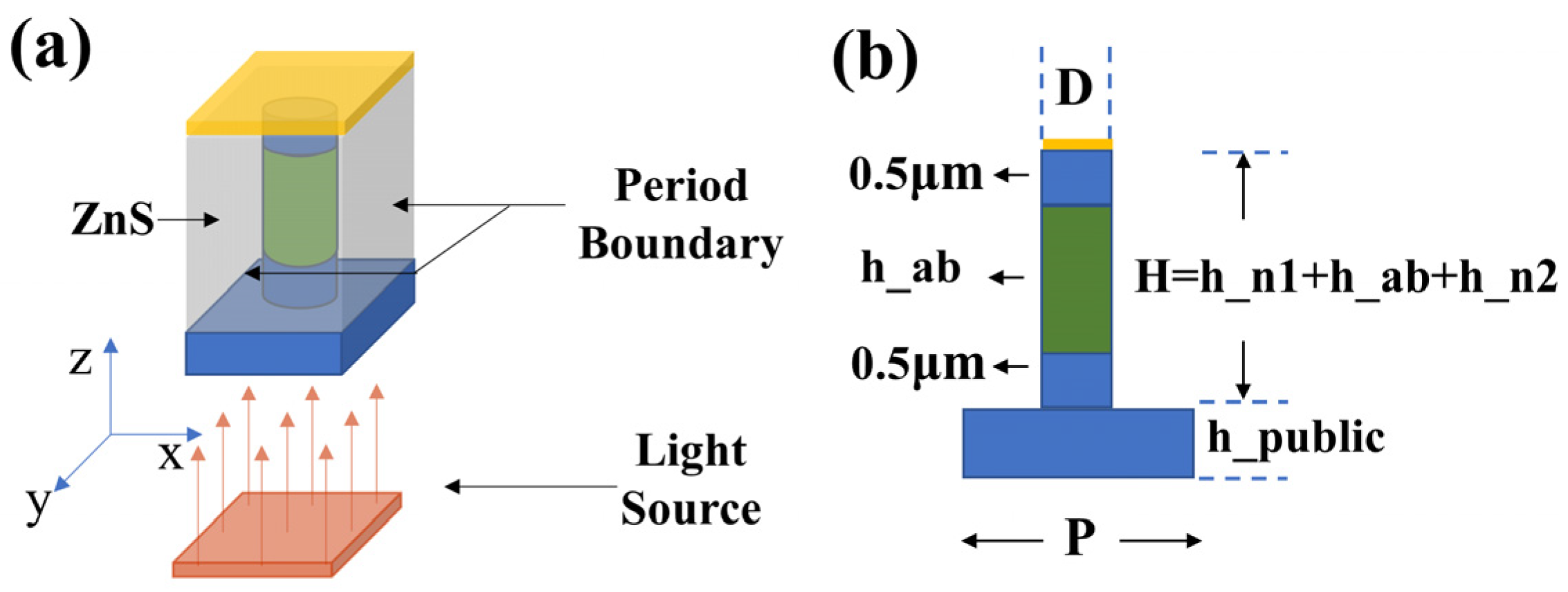
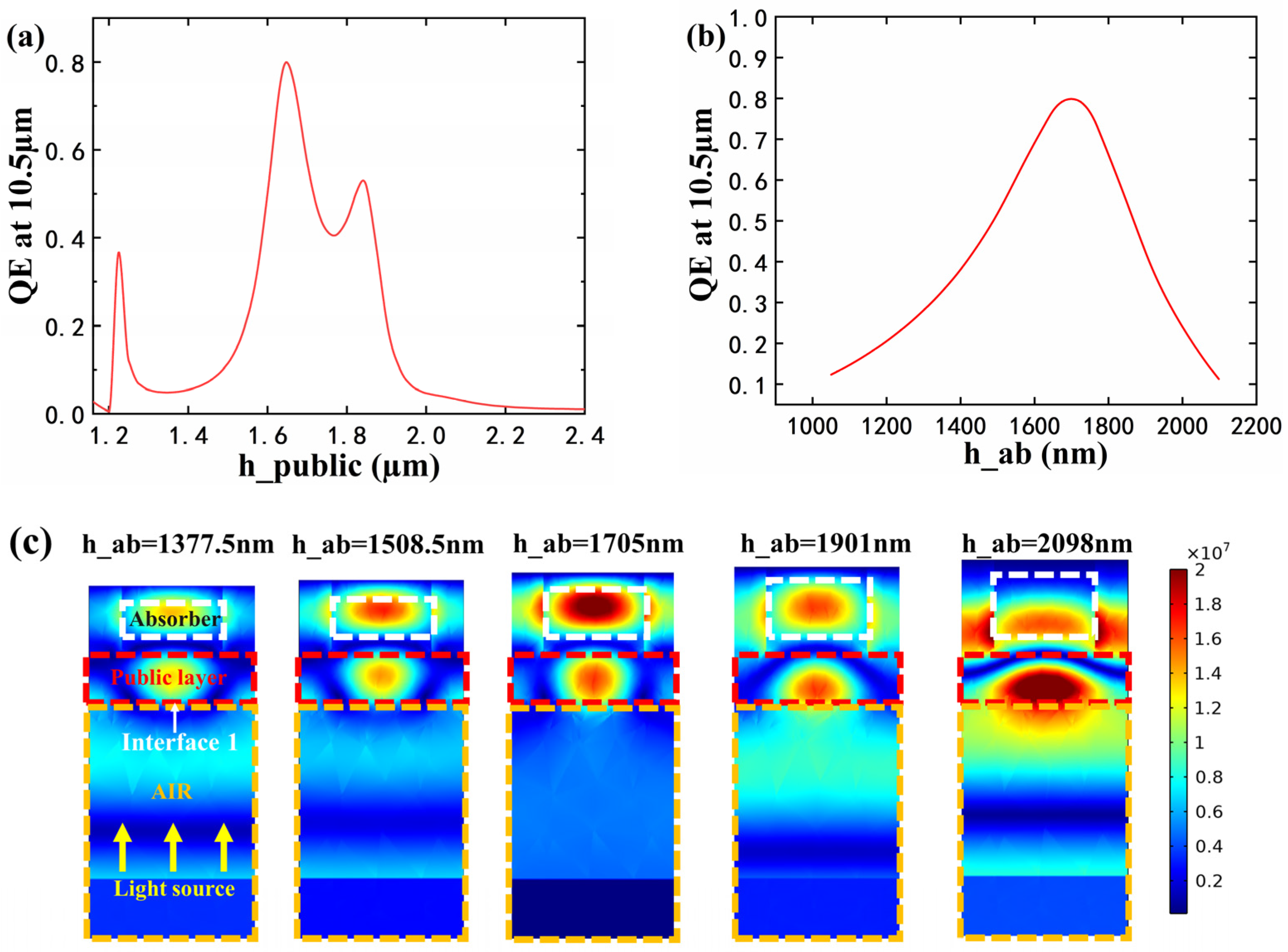
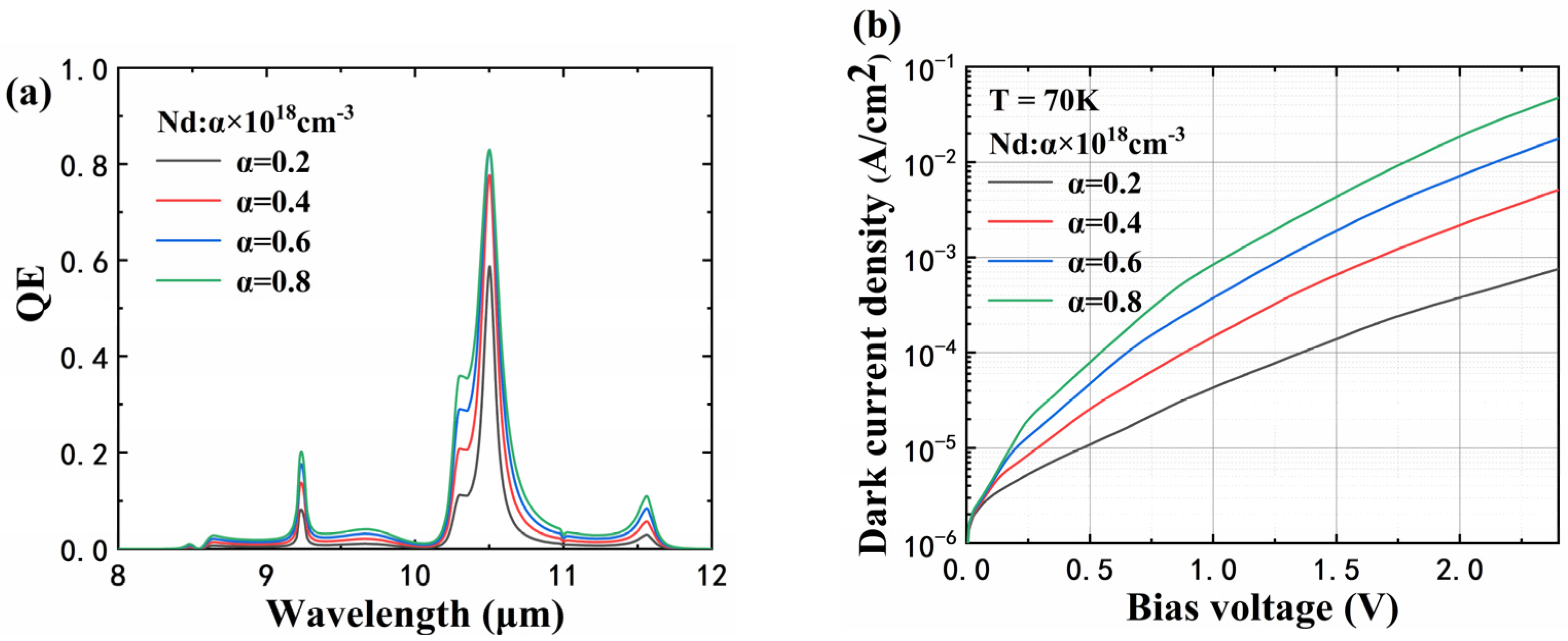
3.2. Quantum Well Micropillar Array with Resonance-Enhanced and Antireflection Effects Targeting at 10.5 μm Central Wavelength
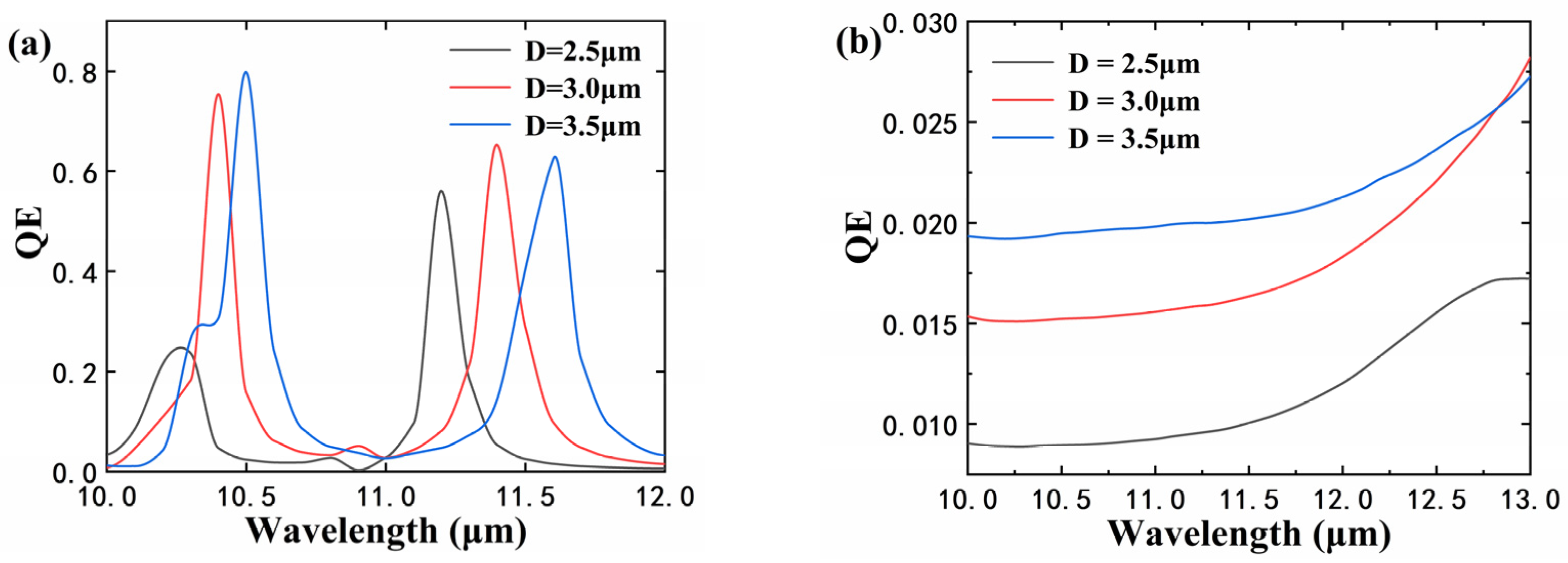
3.3. Performance of the Final Device
4. Conclusions
Author Contributions
Funding
Data Availability Statement
Acknowledgments
Conflicts of Interest
References
- Zhang, X.; Zhang, Y.; Tang, J.; Cui, Z.; Li, Y.; Zhou, H.; Zhang, G.; Yang, J. Optical technology for detecting the decomposition products of SF6: A review. Opt. Eng. 2018, 57, 110901. [Google Scholar] [CrossRef]
- Bai, X.; Bai, P.; Li, X.; Huang, S.; Lian, X.; Song, W.; Shi, Z.; Shen, W.; Zhang, Y. Optical coupling enhancement of multi-color terahertz quantum well detector. J. Appl. Phys. 2021, 130, 203102. [Google Scholar] [CrossRef]
- Shao, D.; Fu, Z.; Tan, Z.; Wang, C.; Qiu, F.; Gu, L.; Wan, W.; Cao, J. Research Progress on Terahertz Quantum-Well Photodetector and Its Application. Front. Phys. 2021, 9, 581. [Google Scholar] [CrossRef]
- Soibel, A.; Bandara, S.V.; Ting, D.Z.; Liu, J.K.; Mumolo, J.M.; Rafol, S.B.; Johnson, W.R.; Wilson, D.W.; Gunapala, S.D. A super-pixel QWIP focal plane array for imaging multiple waveband temperature sensor. Infrared Phys. Technol. 2009, 52, 403–407. [Google Scholar] [CrossRef]
- Xiangyang, L.; Ning, L.; Jintong, X.; Kaihui, C.; Guoqing, X.; Ling, W.; Yan, Z.; Longyuan, Z.; Jiqiang, W.; Wei, L. GaAs/AlGaAs QWIP IRFPA for 10.55 μm long wavelength. Infrared Laser Eng. 2020, 49, 6. [Google Scholar]
- Engelmann, S.U.; Wise, R.S.; Sun, J.; Choi, K.K.; DeCuir, E.A.; Olver, K.A.; Fu, R.X. Design and fabrication of resonator-QWIP for SF6 gas sensor application. In Proceedings of the Advanced Etch Technology for Nanopatterning VI, San Jose, CA, USA, 26 February–2 March 2017. [Google Scholar]
- Smuk, S.; Ivanov, R.; Evans, D.; Sehlin, S.; Diel, W.; Hellström, S.; Höglund, L.; Smuk, A.; Costard, E.; Fulop, G.F.; et al. QWIPs are keeping their promises. In Proceedings of the Infrared Technology and Applications XLV, Baltimore, MD, USA, 14–18 April 2019. [Google Scholar]
- Ivanov, R.; Evans, D.; Smuk, S.; Diel, W.; Rihtnesberg, D.; Höglund, L.; Gulde, M.; Costard, E.; Fulop, G.F.; Kimata, M.; et al. QWIP as solution for mobile VLWIR imaging systems. In Proceedings of the Infrared Technology and Applications XLVII, Online, 12–16 April 2021. [Google Scholar]
- Kim, H.; Ahn, S.-Y.; Wasilewski, Z. Fabrication of grating coupled GaAs/AlGaAs quantum well infrared photodetector on an Si substrate. J. Vac. Sci. Technol. B 2019, 37, 031209. [Google Scholar] [CrossRef]
- Hainey, M.F.; Mano, T.; Kasaya, T.; Jimba, Y.; Miyazaki, H.; Ochiai, T.; Osato, H.; Watanabe, K.; Sugimoto, Y.; Kawazu, T.; et al. Patchwork metasurface quantum well photodetectors with broadened photoresponse. Opt. Express 2021, 29, 59–69. [Google Scholar] [CrossRef]
- Hainey, M.F.; Mano, T.; Kasaya, T.; Ochiai, T.; Osato, H.; Watanabe, K.; Sugimoto, Y.; Kawazu, T.; Arai, Y.; Shigetou, A.; et al. Near-field resonant photon sorting applied: Dual-band metasurface quantum well infrared photodetectors for gas sensing. Nanophotonics 2020, 9, 4775–4784. [Google Scholar] [CrossRef]
- Chu, Z.; Zhou, Y.; Zhou, J.; Chen, P.; Li, Z.; Lu, W.; Chen, X. Quantum well infrared detectors enhanced by faceted plasmonic cavities. Infrared Phys. Technol. 2021, 116, 103746. [Google Scholar] [CrossRef]
- Liang, B.W.; Huang, C.C.; Chao, S.P.; Kao, K.J.; Simbulan, K.B.; Lan, Y.W.; Kuan, C.H. Responsivity and detectivity enhancements by graphene overlay on normal-incident multicolor quantum grid infrared photodetectors. Opt. Express 2020, 28, 2456–2465. [Google Scholar] [CrossRef]
- Goldberg, A.; Choi, K.K.; Cho, E.; McQuiston, B. Laboratory and field performance of megapixel QWIP focal plane arrays. Infrared Phys. Technol. 2005, 47, 91–105. [Google Scholar] [CrossRef]
- Jhabvala, M.; Choi, K.K.; Monroy, C.; La, A. Development of a 1K × 1K, 8–12 μm QWIP array. Infrared Phys. Technol. 2007, 50, 234–239. [Google Scholar] [CrossRef]
- Andresen, B.F.; Choi, K.K.; Fulop, G.F.; Jhabvala, M.D.; Forrai, D.P.; Norton, P.R.; Waczynski, A.; Sun, J.; Jones, R. Electromagnetic modeling of QWIP FPA pixels. In Proceedings of the Infrared Technology and Applications XXXVII, Orlando, FL, USA, 25–29 April 2011. [Google Scholar]
- Choi, K.-K.; Jhabvala, M.D.; Forrai, D.P.; Waczynski, A.; Sun, J.; Jones, R. Electromagnetic Modeling of Quantum Well Infrared Photodetectors. IEEE J. Quantum Electron. 2012, 48, 384–393. [Google Scholar] [CrossRef]
- Kwong-Kit, C.; Jhabvala, M.D.; Forrai, D.P.; Waczynski, A.; Sun, J.; Jones, R. Electromagnetic Modeling and Design of Quantum Well Infrared Photodetectors. IEEE J. Sel. Top. Quantum Electron. 2013, 19, 1–10. [Google Scholar] [CrossRef]
- Hainey, M.F.; Mano, T.; Kasaya, T.; Jimba, Y.; Miyazaki, H.; Ochiai, T.; Osato, H.; Sugimoto, Y.; Kawazu, T.; Shigetou, A.; et al. Breaking the interband detectivity limit with metasurface multi-quantum-well infrared photodetectors. Opt. Express 2021, 29, 43598–43611. [Google Scholar] [CrossRef]
- Yang, K.; Ni, B.; Ge, H.; Zhang, L.; Yang, L.; Ni, H.; Tai, G.; Chang, J. A high-performance quantum well infrared photodetector based on semiconductor–metal periodic microstructure. Opt. Quantum Electron. 2021, 53, 160. [Google Scholar] [CrossRef]
- Liu, L.; Chen, Y.; Huang, Z.; Du, W.; Zhan, P.; Wang, Z. Highly efficient metallic optical incouplers for quantum well infrared photodetectors. Sci. Rep. 2016, 6, 30414. [Google Scholar] [CrossRef] [Green Version]
- Shao, H.; Cheng, B.; Xu, Y.; Song, G. Ultrahigh-quantum-efficiency and high-bandwidth nanowire array UTC-PDs working at 1064 nm. Opt. Quantum Electron. 2022, 54, 15. [Google Scholar] [CrossRef]
- Karimi, M.; Heurlin, M.; Limpert, S.; Jain, V.; Zeng, X.; Geijselaers, I.; Nowzari, A.; Fu, Y.; Samuelson, L.; Linke, H. Intersubband Quantum Disc-in-Nanowire Photodetectors with Normal-Incidence Response in the Long-Wavelength Infrared. Nano Lett. 2017, 18, 365–372. [Google Scholar] [CrossRef] [Green Version]
- Xin-Hui, Y.; Tian, X.; Hui, X.; Xi-ren, C.; Ju-Zhu, L. Quantum well micropillar arrays with low filling factor for enhanced infrared absorption. J. Infrared Millim. Waves 2021, 40, 1. [Google Scholar]
- Choi, K.K.; Allen, S.C.; Sun, J.G.; DeCuir, E.A. Resonant detectors and focal plane arrays for infrared detection. Infrared Phys. Technol. 2017, 84, 94–101. [Google Scholar] [CrossRef]
- Choi, K.K.; Dang, G.; Little, J.W.; Leung, K.M.; Tamir, T. Quantum grid infrared spectrometer. Appl. Phys. Lett. 2004, 84, 4439–4441. [Google Scholar] [CrossRef]
- Zumuukhorol, M.; Khurelbaatar, Z.; Kim, J.-H.; Shim, K.-H.; Lee, S.-N.; Leem, S.-J.; Choi, C.-J. Effect of a SiO2 Anti-reflection Layer on the Optoelectronic Properties of Germanium Metal-semiconductor-metal Photodetectors. J. Semicond. Technol. Sci. 2017, 17, 483–491. [Google Scholar] [CrossRef]
- Rosfjord, K.M.; Yang, J.K.; Dauler, E.A.; Kerman, A.J.; Anant, V.; Voronov, B.M.; Gol’tsman, G.N.; Berggren, K.K. Nanowire single-photon detector with an integrated optical cavity and anti-reflection coating. Opt. Express 2006, 14, 527–534. [Google Scholar] [CrossRef] [PubMed]
- Andresen, B.F.; Ozaki, K.; Fulop, G.F.; Uchiyama, Y.; Nishino, H.; Matsukura, Y.; Kajihara, N.; Fujii, T. Development of mid-wavelength QWIP FPA. In Proceedings of the Infrared Technology and Applications XXXI, Orlando, FL, USA, 28 March–1 April 2005. [Google Scholar]
- Besikci, C. Nature Allows High Sensitivity Thermal Imaging With Type-I Quantum Wells Without Optical Couplers: A Grating-Free Quantum Well Infrared Photodetector With High Conversion Efficiency. IEEE J. Quantum Electron. 2021, 57, 1–12. [Google Scholar] [CrossRef]
- Pan, J.L.; Fonstad, C.G. Theory, fabrication and characterization of quantum well infrared photodetectors. Mater. Sci. Eng. R Rep. 2000, 28, 65–147. [Google Scholar] [CrossRef]


Publisher’s Note: MDPI stays neutral with regard to jurisdictional claims in published maps and institutional affiliations. |
© 2022 by the authors. Licensee MDPI, Basel, Switzerland. This article is an open access article distributed under the terms and conditions of the Creative Commons Attribution (CC BY) license (https://creativecommons.org/licenses/by/4.0/).
Share and Cite
Shao, H.; Xu, Y.; Lv, L.; Cheng, B.; Song, G. Resonance-Enhanced Quantum Well Micropillar Array with Ultra-Narrow Bandwidth and Ultra-High Peak Quantum Efficiency. Electronics 2022, 11, 1396. https://doi.org/10.3390/electronics11091396
Shao H, Xu Y, Lv L, Cheng B, Song G. Resonance-Enhanced Quantum Well Micropillar Array with Ultra-Narrow Bandwidth and Ultra-High Peak Quantum Efficiency. Electronics. 2022; 11(9):1396. https://doi.org/10.3390/electronics11091396
Chicago/Turabian StyleShao, Hanxiao, Yun Xu, Longfeng Lv, Bo Cheng, and Guofeng Song. 2022. "Resonance-Enhanced Quantum Well Micropillar Array with Ultra-Narrow Bandwidth and Ultra-High Peak Quantum Efficiency" Electronics 11, no. 9: 1396. https://doi.org/10.3390/electronics11091396
APA StyleShao, H., Xu, Y., Lv, L., Cheng, B., & Song, G. (2022). Resonance-Enhanced Quantum Well Micropillar Array with Ultra-Narrow Bandwidth and Ultra-High Peak Quantum Efficiency. Electronics, 11(9), 1396. https://doi.org/10.3390/electronics11091396