Article

Anomalous PBTI Effects in N-Type Super Junction under High Gate Voltage Stress

1
School of Microelectronics, Fudan University, Shanghai 200433, China
2
Zhangjiang Fudan International Innovation Center, Shanghai 201203, China
*
Authors to whom correspondence should be addressed.
Electronics 2022, 11(9), 1362; https://doi.org/10.3390/electronics11091362
Submission received: 27 March 2022 / Revised: 19 April 2022 / Accepted: 20 April 2022 / Published: 25 April 2022
(This article belongs to the Section Microelectronics)

Abstract

:
In this work, an anomalous thick oxide-degradation phenomenon in n-type 650-V class super-junction VDMOS transistors is investigated. An unexpected threshold voltage (Vt) decrease was observed with high positive bias temperature instability stress, and the saturation current (IDsat) increases with the stress time. Repeatable and reproducible behaviors have been achieved from multiple devices under test. Based on simulation and experimental results, it is found that the high-energy electrons (caused by high positive gate voltage) in the n-type region at the bottom of the gate oxide layer (top of the N-pillar) are injected into the gate oxide. The high-energy electrons generate electron-hole pairs during the transport to the anode, leaving holes in the gate oxide layer, and thus decreased Vt and increased IDsat. Finally, C-V measurement is also carried out which further confirms the above analysis.

1. Introduction

Super junction (SJ) introduces the PN junction into the conventional “resistive” voltage-resistant layer, turning it into a “junction voltage-resistant layer”. This qualitative change breaks through the “silicon limit” trade-off between the specific on-resistance and withstand voltage of traditional power devices. A thinner drift region and higher doping concentration can achieve lower on-resistance, but the breakdown voltage will decrease accordingly. Super-junction MOSFETs replace the conventional high-resistance with alternating P-pillars and N-pillars in the drift layer. The fixed positive and negative charges left in the depletion region can be mutually depleted when the two-pillar regions are charge-balanced. Therefore, the ionized impurity charge in the drift region does not affect the vertical withstand voltage; so, the pillar region can be doped with a higher concentration under the same withstand voltage [1,2,3].
Nevertheless, SJ devices are usually handled the under extreme condition of higher voltage and heavier current. Such an implementation scenario further highlights the significance of reliability of SJ devices which, however, has rarely been reported. Generally, SJ devices share similar structure as N-type MOSFET at the top, leading to MOS device-based reliability issues. As an important indicator of gate oxide degradation, bias temperature instability (BTI) is critical to the reliability of MOS devices. BTI is typically manifested by the threshold voltage (Vt) shift due to the charge trapping at Si/SiO2 interface which can occur based on Fowler–Nordheim tunneling of the carriers under an external electric field [4,5,6,7,8,9,10,11,12]. Conventionally, Vt of pMOS device shifts to the negative direction after negative BTI (NBTI) stress, and IDsat decreases, while under the action of positive BTI (PBTI) stress, nMOS device’s Vt shifts to the positive direction, and IDsat decreases [13,14,15].
In this study, a 650-V class SJ device is designed and fabricated to study the BTI performance under high gate voltage stress. As compared to the conventional nMOS devices, all devices under test (DUTs) exhibit anomalous and opposite shift behavior in both Vt and IDsat. Based on simulation and experimental analysis, the degradation mechanism is proposed, and C-V measurement is further performed further supporting the analysis.

2. Result and Discussion

2.1. Device Structure

Figure 1a shows the structure diagram of the device cell. In the body area of each cell, the P-pillar and N-pillar are aligned alternately. The main feature size and doping concentration of the device are also demonstrated in Figure 1b. For testing convenience, the device is packaged using TO-220 as depicted in Figure 1c. The thickness of the gate oxide layer is 100 nm, with thickness inhomogeneity below 5%.
Figure 2 shows the fundamental electrical performance of the device studied in this work. As shown in Figure 2a with the blocking characteristics, ID rises abruptly with 700 V bias which suggests that the withstand voltage performance of the device meets the design expectations. Capacitance characteristic is shown in Figure 2b, where Ciss is the input capacitor, Coss is the output capacitor, and Crss is the reverse transfer capacitor. It is observed that these capacitances are VD-dependent, with typical values of Ciss = 1819 pF, Coss = 54.35 pF, and Crss = 2.14 pF when VD is 200 V. Transmission characteristic curve (ID-VD curve) is demonstrated in Figure 2c, with ~170 mῼ on-resistance (VGS = 10 V, ID = 7.3 A). Performance comparison between the fabricated structure with other reported devices is shown in Table 1, which shows that the structure fabricated in this work has higher breakdown voltage and relatively lower on-resistance.
The full structure of the 650-V SJ device designed in this work is schematically shown in Figure 2d. The device structure is divided into cell and terminal regions (with only one cell illustrated in the figure). The terminal region is composed of alternating P- and N-pillars and field plates. The terminal region is designed to sustain the transverse electric potential from the edge-drift region of the devices, ensuring that the edge will not break down in advance. It is noted that this 650-V class SJ is fabricated by deep trench etching and epitaxial growth manufacture process. A trench with a certain aspect ratio is formed by etching, followed by P-type silicon epitaxial growth filling the trench and surface planarization. An n-type layer was formed at the top of N-pillars to further reduce the on-resistance.

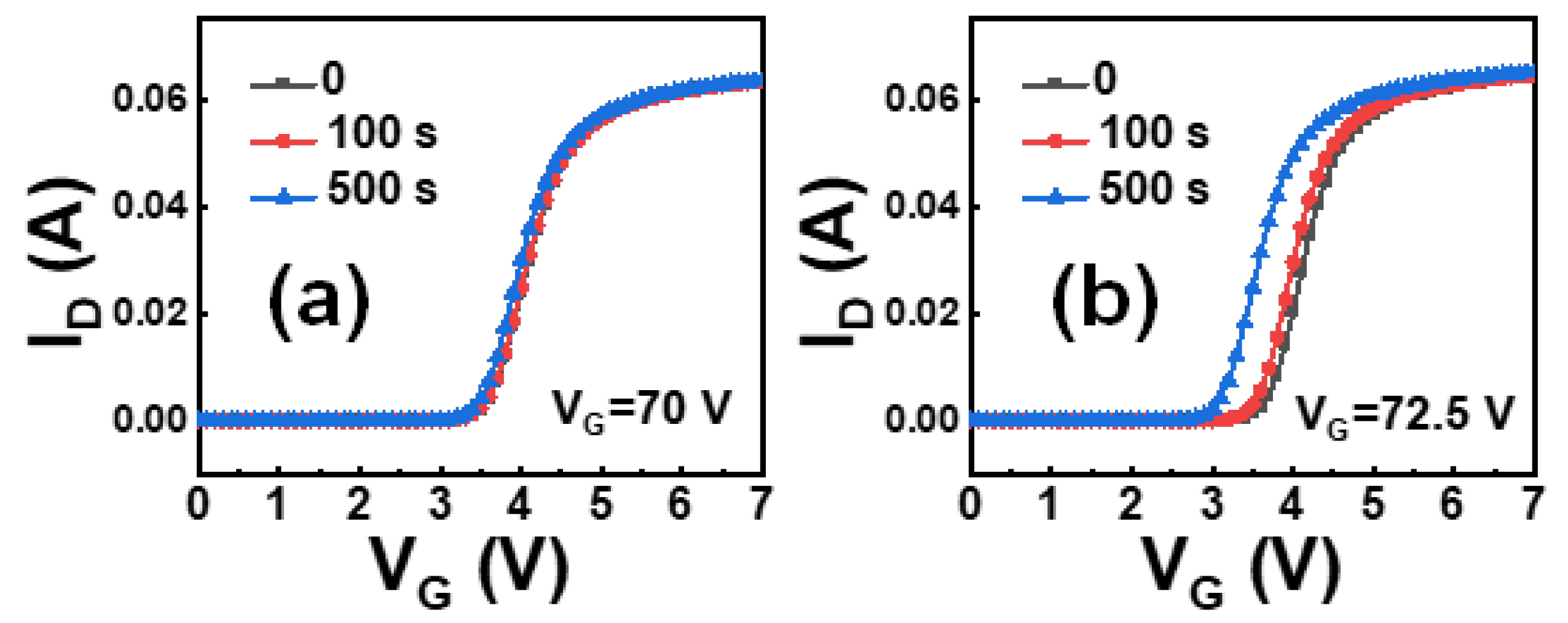
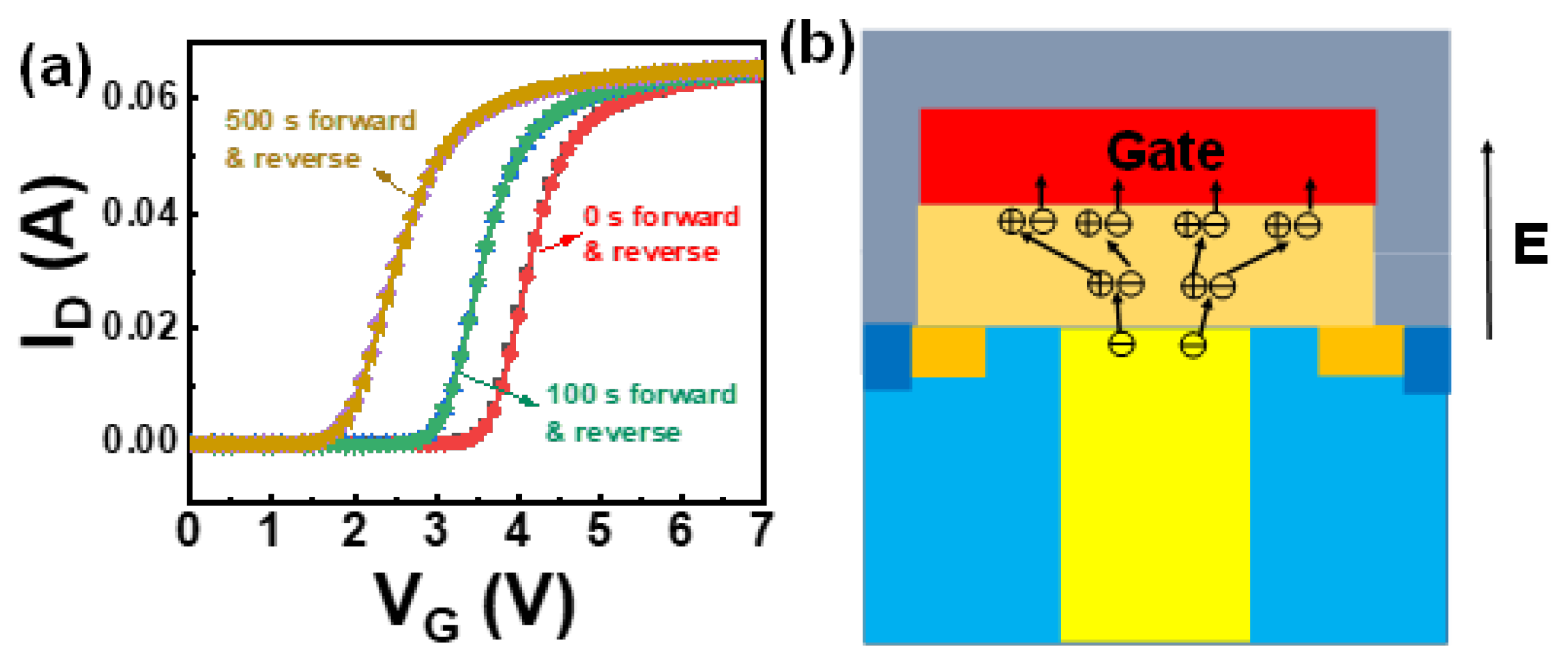
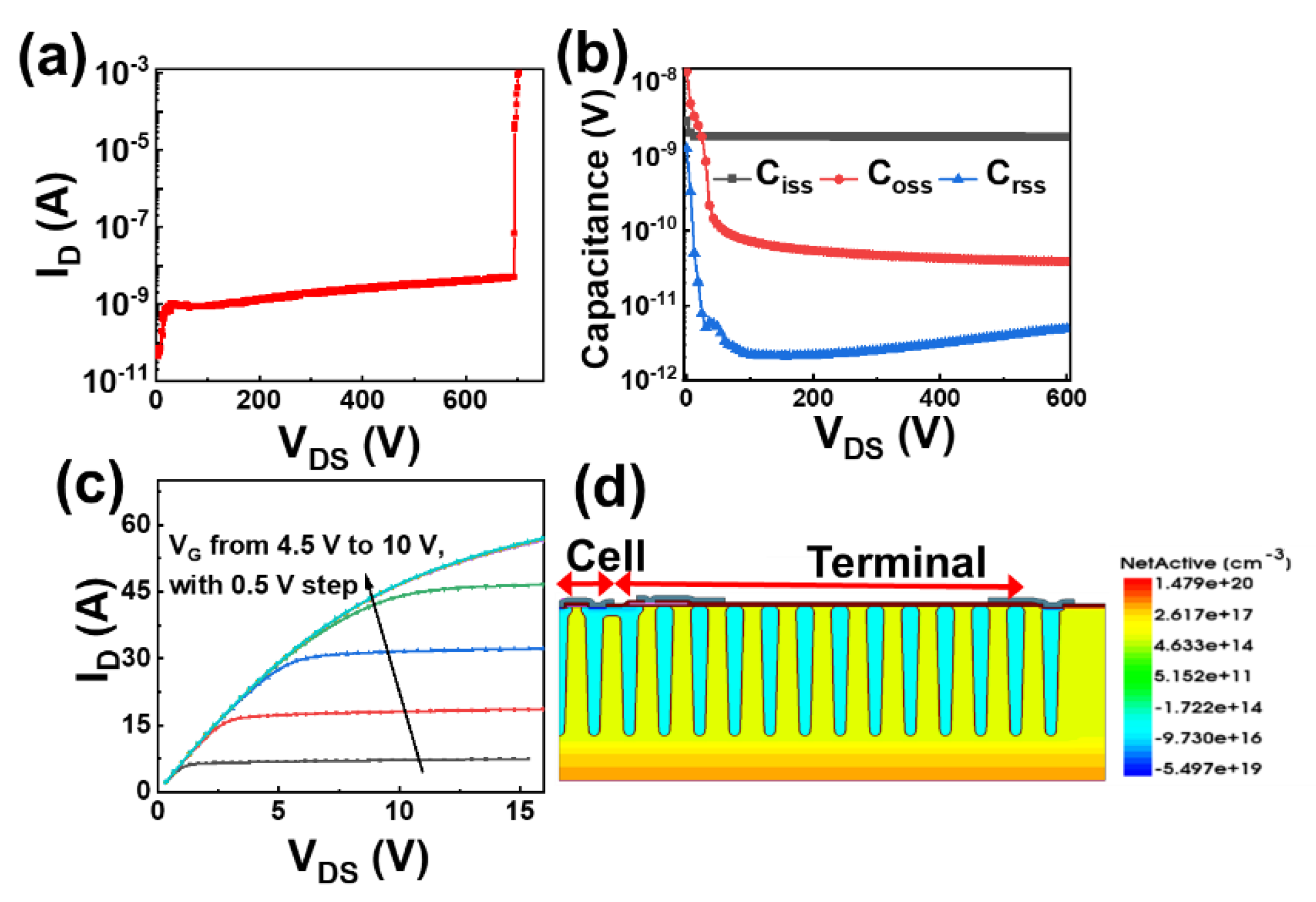
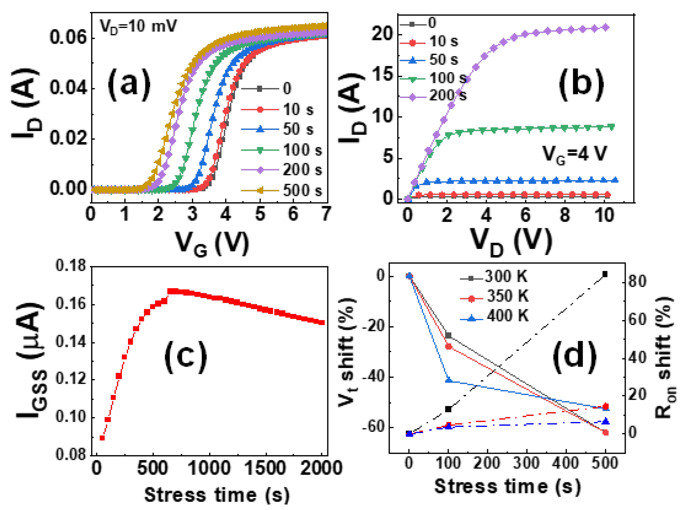
2.2. Measurement Results and Analysis

Figure 3a,b shows the ID-VG and ID-VD curves obtained after different stress time using the stress condition of VG = 75 V and VDS = 0 V. Here, the stress voltage of 75 V is much higher than the operation voltage under normal conditions, and this is based on the consideration of extreme cases with driving circuit chip failure. Under such circumstances, the high voltage from the drain terminal leaks to the gate, and the voltage between the gate and source rises to a much higher value.
From Figure 3a,b, a clear shift towards negative direction is observed in Vt, and IDsat increases with longer stress time. The increase in IDsat is actually due to the decrease in threshold voltage in the initial stage of stress. It is noted that a similar trend has been obtained from multiple devices in this study. Such behavior is opposite to the performance of traditional MOSFET devices under the PBTI stress, as well as previous studies on the PBTI effect of VDMOS devices [13,14]. Figure 3c shows the change in gate current with increasing stress time. IGSS shows a relatively rapid increase in the first ~500 s stress followed by a slower decrease with longer stress time. It is worth mentioning that there are some discontinuities in the IGSS curve at 700 s, which may be caused by the error of the test system (such as jitter).
Figure 3d summarizes and compares the threshold voltage and saturation current degradation behaviors under different temperatures of 300 K, 350 K, and 400 K. It is observed that high temperature can accelerate the degradation of the threshold voltage of the device at the initial stage of stress. When the stress time is greater than 500 s, the degradation level is basically the same, indicating that the effect of stress on device performance is gradually saturated. It is worth mentioning that initial and final I-V characteristics were measured at room and stress temperatures, but all other interim measurements were performed only at stress temperature in order to minimize the recovery effects.
Threshold voltage shifts under different gate voltage stresses are further studied. As shown in Figure 4, under lower forward voltages of 70 V (Figure 4a) and 72.5 V (Figure 4b), the ID-VG curves show the same shift trend. Specifically, with a 70-V forward voltage stress, negligible shifting is observed in the transfer curve with different stress time. As compared to the 75-V gate voltage stress shown in Figure 3a, a higher stress voltage level introduces a more significant Vt degradation. It is also observed that the device properties did not recover after prolonged standing after the stress, indicating that the degradation caused by stress is irreversible.

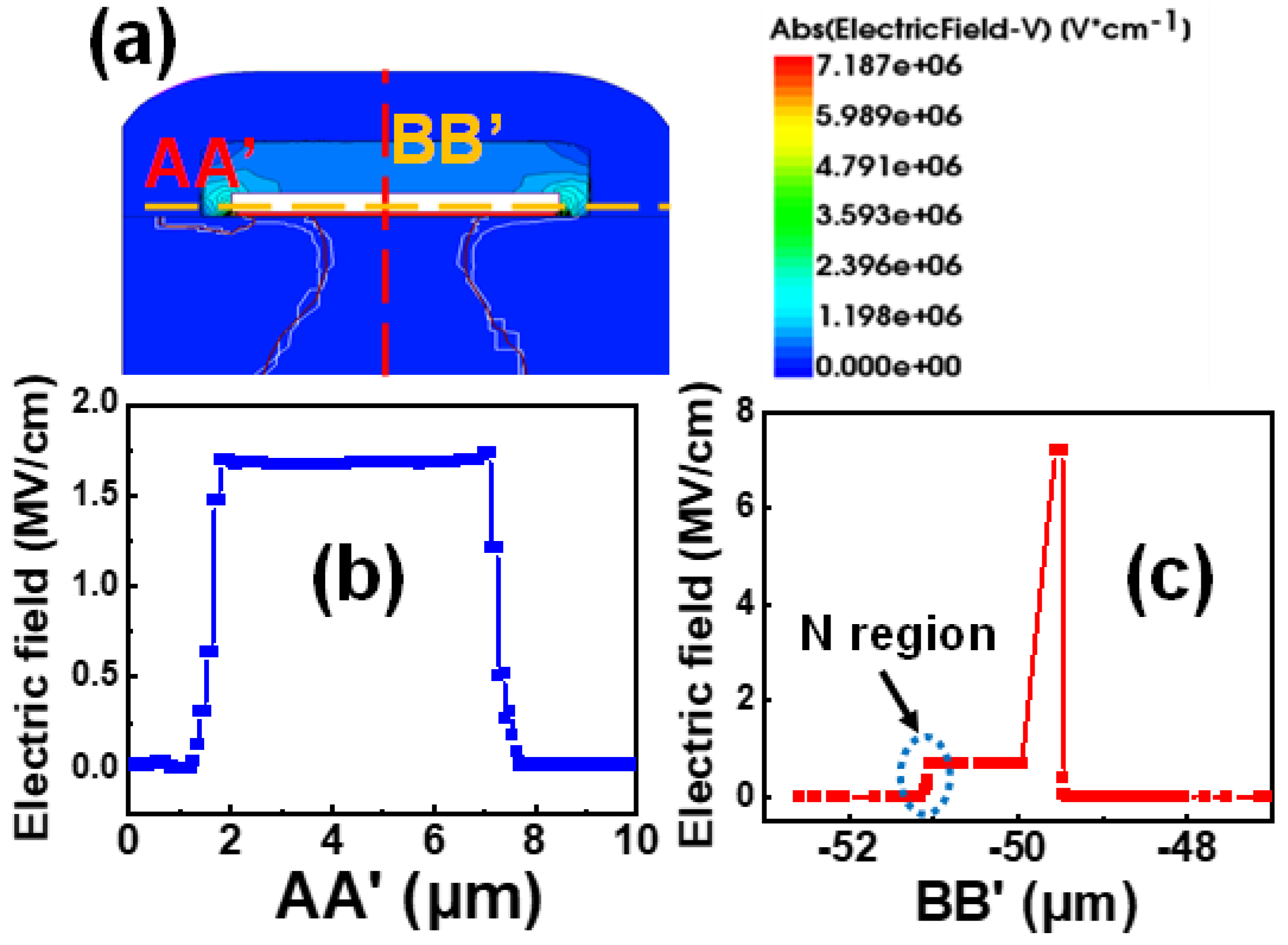
2.3. Mechanism Explanation

We first characterize the electric field distribution by using Sentaurus TCAD tools, which is shown in Figure 5a. The electric fields along the AA’ and BB’ (indicated in Figure 5a) are shown in Figure 5b,c, respectively. It is observed that under high positive gate voltage stress, the electric field in the N-type region under the gate oxide layer is sufficiently high, and hot electrons are generated which can easily be injected into the gate oxide layer.
Compared with traditional N-type MOS devices, the bottom of the gate oxide layer of an SJ device is mainly an N-type region. During the fabrication process, the doping concentration of the N-type region at the bottom of the gate oxide layer is generally higher than that of the N-pillar region in order to reduce the on-resistance of the device. To further study the mechanism of degradation, the ID-VG sweep in the forward and reverse directions are measured with 75-V stress voltage and different stress time. As depicted in Figure 6a, no hysteresis is observed between the forward and reverse curves for all the tested stress times, indicating no extra movable charges inside the gate oxide layer, and no fixed charges are generated under high gate stress voltage.
Figure 6b schematically shows the generation and transport of the carriers in the SJ cell. Under the application of a large electric field, the high gate voltage causes generation of more high-energy electrons in the N-type region at the top of the N-pillar. With high forward voltage, a large number of high-energy electrons is injected into the gate oxide. These high-energy electrons reach the anode under the electric field in the oxide layer and obtain a certain kinetic energy. At the same time, some of the high-energy electrons collide during the movement to generate electron-hole pairs. Most electrons reach the anode under the application of electric field. However, defects exist in SiO2, such as silicon dangling bonds and micropores, which can evolve into adsorption centers trapping holes. This process is equivalent to injection of holes into the oxide layer, resulting in a shift in Vt, and an increase in IDsat. The degradation mechanism is related to hot carriers and tunneling instead of the hot holes. This is because the stress condition is the high positive gate voltage, and the electric field is preventing holes injecting into the gate oxide layer. In addition, the energy required for hole tunneling is larger, and the P-type region (hole-generating region) at the bottom of the gate is smaller than the N-type region (electron-generating region).
We have also tested the change in gate current when increasing VG from 0 V to 75 V. During VG ramping, the gate current is maintained below 500 pA and slowly increases, reaching 1.5 nA at 75 V finally. Considering the fact that there is no carrier inside the gate oxide layer, avalanche carriers cannot be generated by themselves, and the avalanche carriers that tunnel into the gate oxide are mainly generated at the bottom of the gate oxide. To further verify the degradation mechanism, C-V measurement is performed. Figure 7a–c shows the C-V curves obtained at 100-kHz frequency under PBTI stress with voltage of 70 V, 72.5 V, and 75 V. Under all stress conditions, the devices show a clear left shift in the C-V curves, which indicates extra positive charge generation in the gate oxide above the channel region. The C-V measurement result is consistent with the above analysis. At a higher gate voltage, more positive charges generated inside the oxide, the drift phenomenon is more obvious.
At the same time, it was found that in the process of stress, additional interface states are generated at the bottom of the gate oxide layer of the device, which are mainly caused by defects or surface states generated at the interface during the process of electron tunneling to the gate oxide layer. Such defects can lead to the bumps observed in the C-V curves as shown in Figure 7. A similar phenomenon is also observed when scanning the C-V curve under higher frequency of 1 MHz, suggesting that the resulting interface state can respond to at least 1-MHz frequency.

3. Conclusions

A 650-V class SJ MOSFET device is designed and fabricated. Anomalous Vt decrease behavior is observed with PBTI stress, and an increase in IDsat with the stress time is presented. Experimental and theoretical analyses have been performed seeking the mechanism, and it is concluded that the high-energy electrons caused by high positive gate voltage in the N-type region at the bottom of the gate oxide layer (top of the N-pillar) are injected into the gate oxide. The high-energy electrons generate electron-hole pairs in the process of moving to the anode. The electrons reach the anode and the holes remain in the gate oxide layer. As a result, the threshold voltage decreases and the saturation current increases. Such behavior and underlying principles are further verified and confirmed by C-V measurements. Our results can be instructive in future optimization of advanced power device design and engineering.

Author Contributions

Writing—original draft, H.T. and H.X.; validation, H.X. and H.Z.; writing—review and editing, L.C. and H.Z; supervision, Q.S. All authors have read and agreed to the published version of the manuscript.

Funding

This work was supported by the Science and Technology Commission of Shanghai Municipality (20501130202 and 21DZ1100700), the Open Research Fund of State Key Laboratory of Bioelectronics, Southeast University, and the young scientist project of MOE innovation platform.

Data Availability Statement

The data presented in this study are available on request from the corresponding author.

Conflicts of Interest

The authors declare no conflict of interest.

References

  1. Kobayashi, T.; Abe, H.; Niimura, Y.; Yamada, T.; Kurosaki, A.; Hosen, T.; Fujihira, T. High-voltage power MOSFETs reached almost to the silicon limit. In Proceedings of the 13th International Symposium on Power Semiconductor Devices & ICs. IPSD’01, Osaka, Japan, 4–7 June 2001. [Google Scholar] [CrossRef]
  2. Lorenz, L.; Deboy, G.; Knapp, A.; Marz, M. COOLMOS/sup TM/-a new milestone in high voltage power MOS. In Proceedings of the 11th International Symposium on Power Semiconductor Devices and ICs, Toronto, ON, Canada, 26–28 May 1999; pp. 3–10. [Google Scholar] [CrossRef]
  3. Saito, W.; Omura, I.; Aida, S.; Koduki, S.; Izumisawa, M.; Ogura, T. Semisuperjunction MOSFETs: New design concept for lower on-resistance and softer reverse-recovery body diode. IEEE Trans. Electron Devices 2003, 50, 1801–1806. [Google Scholar] [CrossRef]
  4. Cheng, B.; Brown, A.R.; Asenov, A. Impact of NBTI/PBTI on SRAM Stability Degradation. IEEE Electron Device Lett. 2011, 32, 740–742. [Google Scholar] [CrossRef]
  5. Denais, M.; Huard, V.; Parthasarathy, C.; Ribes, G.; Perrier, F.; Revil, N.; Bravaix, A. Interface Trap Generation and Hole Trapping Under NBTI and PBTI in Advanced CMOS Technology With a 2-nm Gate Oxide. IEEE Trans. Device Mater. Reliab. 2004, 4, 715–722. [Google Scholar] [CrossRef]
  6. Zafar, S.; Kim, Y.; Narayanan, V.; Cabral, C.; Paruchuri, V.; Doris, B.; Stathis, J.; Callegari, A.; Chudzik, M. A Comparative Study of NBTI and PBTI (Charge Trapping) in SiO2/HfO2 Stacks with FUSI, TiN, Re Gates. In Proceedings of the 2006 Symposium on VLSI Technology, Honolulu, HI, USA, 13–15 June 2006. [Google Scholar] [CrossRef]
  7. Cartier, E.; Frank, M.M.; Ando, T.; Rozen, J.; Narayanan, V. PBTI in InGaAs MOS capacitors with Al2O3/HfO2/TiN gate stacks: Interface-state generation. In Proceedings of the 2018 IEEE International Reliability Physics Symposium (IRPS), Burlingame, CA, USA, 11–15 March 2018; pp. 5A.4-1–5A.4-4. [Google Scholar] [CrossRef]
  8. Rauch, S.E. Review and Reexamination of Reliability Effects Related to NBTI-Induced Statistical Variations. IEEE Trans. Device Mater. Reliab. 2007, 7, 524–530. [Google Scholar] [CrossRef]
  9. Zhang, J.; Eccleston, W. Positive bias temperature instability in MOSFETs. IEEE Trans. Electron Devices 1998, 45, 116–124. [Google Scholar] [CrossRef]
  10. Cartier, E.; Linder, B.P.; Narayanan, V.; Paruchuri, V.K. Fundamental understanding and optimization of PBTI in nFETs with SiO2/HfO2 gate stack. In Proceedings of the 2006 International Electron Devices Meeting, San Francisco, CA, USA, 11–13 December 2006; pp. 1–4. [Google Scholar] [CrossRef]
  11. Cartier, E.; Kerber, A. Stress-induced leakage current and defect generation in nFETs with HfO2/TiN gate stacks during positive-bias temperature stress. In Proceedings of the IEEE International Reliability Physics Symposium, Montreal, QC, Canada, 26–30 April 2009; pp. 486–492. [Google Scholar]
  12. Zhao, K.; Stathis, J.; Linder, B.P.; Cartier, E.; Kerber, A. PBTI under dynamic stress: From a single defect point of view. In Proceedings of the 2011 International Reliability Physics Symposium, Monterey, CA, USA, 10–14 April 2011; pp. 4A.3.1–4A.3.9. [Google Scholar] [CrossRef]
  13. Alwan, M.; Beydoun, B.; Ketata, K.; Zoaeter, M. Bias temperature instability from gate charge characteristics investigations in n-channel power MOSFET. Microelectron. J. 2007, 38, 727–734. [Google Scholar] [CrossRef]
  14. Alwan, M.; Beydoun, B.; Ketata, K.; Zoaeter, M. Gate charge behaviors in N-channel power VDMOSFETs during HEF and PBT stresses. Microelectron. Reliab. 2007, 47, 1406–1410. [Google Scholar] [CrossRef]
  15. Saito, W.; Omura, I.; Aida, S.; Koduki, S.; Izumisawa, M.; Yoshioka, H.; Okumura, H.; Yamaguchi, M.; Ogura, T. A 15.5m Ω cm2-680V Superjunction MOSFET Reduced On-Resistance by Lateral Pitch Narrowing. In Proceedings of the 2006 IEEE International Symposium on Power Semiconductor Devices and IC’s, Naples, Italy, 4–8 June 2006. [Google Scholar] [CrossRef]
  16. Moens, P.; Bogman, F.; Ziad, H.; De Vleeschouwer, H.; Baele, J.; Tack, M.; Loechelt, G.; Grivna, G.; Parsey, J.; Wu, Y.; et al. UltiMOS: A local charge-balanced trench-based 600V super-junction device. In Proceedings of the 2011 IEEE 23rd International Symposium on Power Semiconductor Devices and IC’s, San Diego, CA, USA, 23–26 May 2011; pp. 304–307. [Google Scholar] [CrossRef]
  17. Lee, S.C.; Oh, K.-H.; Kim, S.S.; Yun, C.M. 650V superjunction MOSFET using universal charge balance concept through drift region. In Proceedings of the 2014 IEEE 26th International Symposium on Power Semiconductor Devices & IC’s (ISPSD), Waikoloa, HI, USA, 15–19 June 2014; pp. 83–86. [Google Scholar] [CrossRef]
  18. Sugi, A.; Takei, M.; Takahashi, K.; Yajima, A.; Tomizawa, H.; Nakazawa, H. Super Junction MOSFETs above 600V with Parallel Gate Structure Fabricated by Deep Trench Etching and Epitaxial Growth. In Proceedings of the 2008 20th International Symposium on Power Semiconductor Devices and IC’s, Orlando, FL, USA, 18–22 May 2008; pp. 165–168. [Google Scholar] [CrossRef]
  19. Ono, S.; Saito, W.; Takashita, M.; Kurushima, S.; Tokano, K.; Yamaguchi, M. Design concept of n-buffer layer (n-Bottom Assist Layer) for 600V-class Semi-Super Junction MOSFET. In Proceedings of the 19th International Symposium on Power Semiconductor Devices and IC’s, Jeju, Korea, 27–30 May 2007; pp. 25–28. [Google Scholar] [CrossRef]
  20. Sentaurus™ Process User Guide, Version N-2017.09; Synopsys, Inc.: Mountain View, CA, USA, 2017.
Figure 1. (a) Schematic of the 650-V SJ cell structure. (b) Main device parameter. (c) Photograph of a packaged SJ device.
Electronics 11 01362 g001
Figure 2. (a) Blocking and (b) capacitance characteristics. (c) ID-VD curves under various VG voltages. (d) Schematic of full structure of the designed 650-V SJ device.
Electronics 11 01362 g002
Figure 3. (a) ID-VG and (b) ID-VD curves obtained after different gate stress time. (c) Variation of IGSS with stress time. (d) Shift of Vt and on-state resistance as a function of stress time at different temperatures (300 K, 350 K, and 400 K).
Electronics 11 01362 g003
Figure 4. ID-VG curves measured after stress time of 0 s, 100 s, and 500 s with (a) VG = 70 V and (b) VG = 72.5 V.
Electronics 11 01362 g004
Figure 5. (a) Simulated electric field distribution of the designed device cell. (b) Electric field distribution along AA’. (c) Electric field distribution along BB’.
Electronics 11 01362 g005
Figure 6. (a) Forward and reverse ID-VG curves after stress time of 0 s, 100 s, and 500 s with VD = 0.01 V. (b) Mechanism of device performance degradation.
Electronics 11 01362 g006
Figure 7. Variations of C-V curves measured at 100 kHz with (a) 70 V, (b) 72.5 V, and (c) 75 V stress voltage after stress time of 0 s, 100 s, and 500 s. (d) Variations of C-V curves (1 MHz) with 75-V gate voltage after stress time of 0 s, 100 s, and 500 s.
Electronics 11 01362 g007
Table 1. Comparison of the performance of the fabricated device with similar devices.
Ref.BVRon
[16]680 V15.5 mΩ·cm2
[17]730 V23 mΩ·cm2
[18]650 V24.7 mΩ·cm2
[19]650 V17 mΩ·cm2
[20]750 V24.6 mΩ·cm2
Proposed700 V17.5 mΩ·cm2
Publisher’s Note: MDPI stays neutral with regard to jurisdictional claims in published maps and institutional affiliations.

