
An Efficient Crypto Processor Architecture for Side-Channel Resistant Binary Huff Curves on FPGA


 , , , and
Abstract
:1. Introduction
1.1. Algorithmic Evolution of BHC Model of ECC and the Corresponding Hardware Accelerators
1.2. Limitations in the Existing Architectures
1.3. Novelty and Contributions
- Crypto processor architecture: We have presented an area-optimized FPGA-based crypto processor architecture responsible for accelerating the PM of the BHC model of ECC over .
- Design trade-offs for various multipliers: For performance and area trade-offs of polynomial multipliers, we have implemented six different multiplication architectures: (1) schoolbook, (2) hybrid Karatsuba, (3) 2-way-karatsuba, (4) 3-way-toom-cook, (5) 4-way-toom-cook and (6) digit-parallel-least-significant, in a Verilog HDL.
- Design trade-offs for BHC model of ECC: We have integrated each polynomial multiplication architecture in our novel BHC processor architecture for design trade-offs (or performance evaluations), concerning hardware resource utilization, clock frequency, latency (time for execution of one PM) and consumed power.
- Finally, a dedicated controller is utilized for the management and coordination of various processing tasks.
2. Related Background
2.1. Bhc over
2.2. Point Multiplication
| Algorithm 1: Double and Add PM Algorithm [17,19,20] |
Input: with , Output: 1 , , , , 2 for(i from m-1 down to 0)do 3 , 4 if , then 5 , 6 end 7 end if 8 end for 9 end 10 |
2.3. Unified Addition Law () of BHC
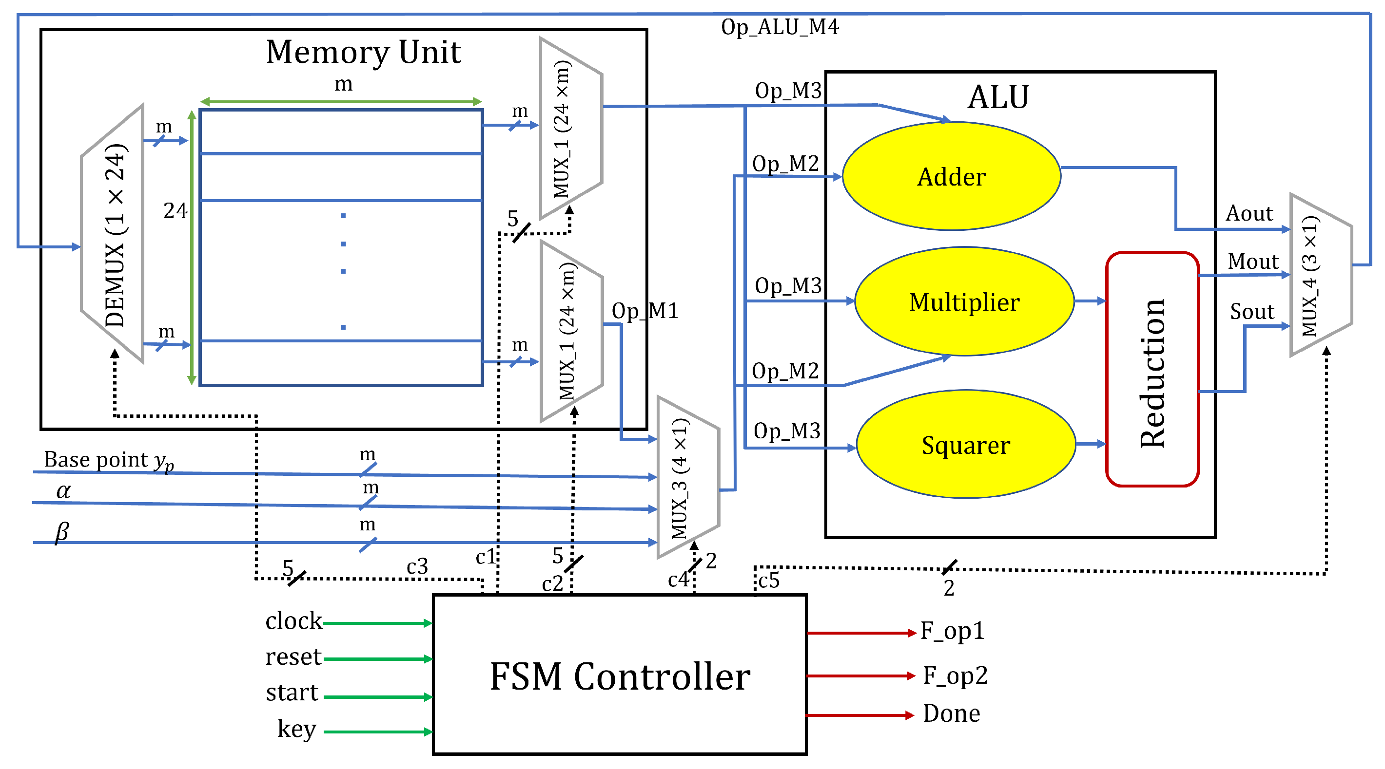
3. Proposed Architecture
3.1. Memory Unit (MU)
3.2. Routing Multiplexers
3.3. Arithmetic and Logic Unit
3.3.1. Adder and Squarer Units
3.3.2. Multiplier Unit
- Schoolbook multiplier: The multiplication using the schoolbook method is executed by generating simple partial products. After generating partial products, shift and add operations are used yielding a result of size bits. A total of clock cycles are needed to perform one multiplication for input operands length of m-bits. Moreover, a schoolbook multiplication method is more convenient to save hardware resources without considering the clock cycles [23].
- Hybrid Karatsuba multiplier: The Karatsuba multiplication method uses the divide and conquer approach for the multiplication of two polynomials each of size m-bits. The divide and conquer approach is performed in chronological order, i.e., polynomial multiplications starting from lower to higher bits. Moreover, the hybrid approach is attained by implementing the simple and general Karatsuba multipliers as used in [13]. A simple Karatsuba multiplier is utilized to perform multiplication over smaller bits, whereas the general Karatsuba multiplier is employed to perform multiplication over longer bits. The objective of using a simple Karatsuba multiplier is the reduction of logic delays, whereas for minimizing the overall gate counts the general Karatsuba multiplier is used. It requires only a single clock cycle for one polynomial multiplication and is more suitable to reduce the latency of the PM operation.
- 2-way-karatsuba multiplier: Two m-bit input polynomials are divided into two sub-polynomials to perform multiplication. The sub-polynomials can then multiplied either by using simple Karatsuba, general Karatsuba, or the schoolbook multiplication method [25]. However, in this work, a schoolbook multiplication method is incorporated to compute the inner products (required to compute in the 2-way-karatsuba). Finally, it requires clock cycles [23,24], when m is the length of the input polynomial or the underlying field.
- 3-way-toom-cook multiplier: In this multiplier, two m-bit input polynomials are divided into three sub-polynomials. The sub-polynomials are then multiplied by using a schoolbook multiplication method to compute the inner products (required to compute in the 3-way-toom-cook). Finally, it requires clock cycles [23], when m is the length of the input polynomials.
- 4-way-toom-cook multiplier: Similar to other multipliers, i.e., 2-way-karatsuba, and 3-way-toom-cook, two m-bit input polynomials are divided into four sub-polynomials to perform multiplication. The sub-polynomials are then multiplied by using a schoolbook multiplication method to compute the inner products (required to compute in the 4-way-toom-cook). Subsequently, it requires clock cycles [24], when m is the length of the input polynomials.
- Least-significant-digit-parallel multiplier: Two input polynomials ( and ) each having size of m-bits, are multiplied by creating digits of polynomial (with size of each digit 32-bits). The input polynomial is multiplied with each created digit of size 32 bits, to produce the resulting polynomials of size bits, where d is the size of a created digit. By using the addition and shifting of polynomials of size bits, the final polynomial generated having a size of bits. Similar to the hybrid Karatsuba multiplier, the digit parallel multiplier takes one clock cycle for computation.
3.3.3. Reduction Unit
3.3.4. Polynomial Inversion Computation
3.4. Control Unit
- Affine to Lopez Dahab projective conversions (States 1 to 3): State 0 is an idle state where none of the operations is performed. From, state 1 to 3, the arithmetic operations involved in line 1 of Algorithm 1 is performed.
- Point doubling states (States 4 to 40): The states from 4 to 40 generates control signals for the computation of point doubling (using a list of instructions shown in column two of Table 2). Moreover, state 40 is responsible to check each bit of k, i.e., (the signal is shown in Figure 2). Once the value for then the next state will be 41, otherwise, the next state will be 4. Additionally, state 40 is also in charge of checking the signal (shown in Figure 2) for counting the number of points on the defined BHC curve. Initially, the value for is set to . Once the value for then the next state will state 78 otherwise the next state will be 4.
- Lopez Dahab to affine coordinate system (States 78 to 99): The states from 78 to 99 generates control signals for the computation of Lopez Dahab to a general affine coordinate system. As shown in line 10 of Algorithm 1, an associated inversion operation is required to perform. Therefore, 78 to 96 states are responsible to perform an inversion operation using the square version of the Itoh-Tsujii algorithm. Furthermore, additional operations of line 10 of Algorithm 1 are implemented from 97 to 99 states.
Clock Cycles Calculation
- Affine to Lopez Dahab projective conversions: As shown in Equation (3), conversions from affine to Lopez Dahab projective coordinate system takes a total of 3 clock cycles.
- Point doubling: The PD requires clock cycles, where determines the clock cycles for 17 multiplication instructions in the of BHC while n presents the clock cycle for one finite field multiplication. Additional 20 clock cycles are needed for the computation of addition and squaring instructions. The value for m presents the key length.
- Point addition: Similarly, the PA requires clock cycles, where determines the clock cycles for the computation of 17 multiplication instructions in the of BHC while n determines the clock cycle for one multiplication. Additional 20 cycles are needed to compute addition and squaring instructions. The value for m shows the key length.
- Lopez Dahab to affine coordinate system: Finally, clock cycles are needed for conversion from Lopez Dahab to affine coordinates. A total of clock cycles are needed for each finite field inversion. In this work, the inversion is computed using a square Itoh-Tsujii inversion algorithm. For the remaining operations in Lopez Dahab to affine coordinate conversions, additional clock cycles are needed.
4. Implementation Results and Comparisons
4.1. Results
4.1.1. Implementations of Polynomial Multipliers
4.1.2. Results for Point Multiplication of BHC
4.2. State-of-the-Art Implementations Comparison
4.2.1. Comparison to of 2011
4.2.2. Comparison to of 2013
4.2.3. Comparison to of 2018
5. Conclusions
Author Contributions
Funding
Institutional Review Board Statement
Informed Consent Statement
Conflicts of Interest
References
- Rashid, M.; Imran, M.; Jafri, A.R.; Al-Somani, T.F. Flexible architectures for cryptographic algorithms—A systematic literature review. J. Circuits Syst. Comput. 2019, 28, 1930003. [Google Scholar] [CrossRef]
- Li, J.; Zhong, S.; Li, Z.; Cao, S.; Zhang, J.; Wang, W. Speed-Oriented Architecture for Binary Field Point Multiplication on Elliptic Curves. IEEE Access 2019, 7, 32048–32060. [Google Scholar] [CrossRef]
- Imran, M.; Rashid, M.; Jafri, A.R.; Kashif, M. Throughput/area optimised pipelined architecture for elliptic curve crypto processor. IET Comput. Digit. Tech. 2019, 13, 361–368. [Google Scholar] [CrossRef] [Green Version]
- Diffie, W.; Hellman, M. New directions in cryptography. IEEE Trans. Inf. Theory 1976, 22, 644–654. [Google Scholar] [CrossRef] [Green Version]
- Rivest, R.L.; Shamir, A.; Adleman, L.M. A method for obtaining digital signatures and public-key cryptosystems. Commun. ACM 1978, 21, 120–126. [Google Scholar] [CrossRef]
- Koblitz, N. Elliptic curve cryptosystems. Math. Comput. 1987, 48, 203–209. [Google Scholar] [CrossRef]
- Miller, V.S. Use of Elliptic Curves in Cryptography. In Advances in Cryptology—CRYPTO ’85 Proceedings; Williams, H.C., Ed.; Springer: Berlin/Heidelberg, Germany, 1986; pp. 417–426. [Google Scholar]
- Imran, M.; Shehzad, F. FPGA Based Crypto Processor for Elliptic Curve Point Multiplication (ECPM) over GF (2233). Int. J. Inf. Secur. Res. 2017, 7, 706–713. [Google Scholar] [CrossRef]
- Hankerson, D.; Menezes, A.J.; Vanstone, S. Guide to Elliptic Curve Cryptography 2004. pp. 1–311. Available online: https://link.springer.com/book/10.1007/b97644 (accessed on 6 March 2022).
- Bernstein, D.J.; Lange, T.; Rezaeian Farashahi, R. Binary edwards curves. In International Workshop on Cryptographic Hardware and Embedded Systems; Springer: Berlin/Heidelberg, Germany, 2008; pp. 244–265. [Google Scholar]
- Farashahi, R.R.; Joye, M. Efficient Arithmetic on Hessian Curves. In Public Key Cryptography—PKC 2010; Nguyen, P.Q., Pointcheval, D., Eds.; Springer: Berlin/Heidelberg, Germany, 2010; pp. 243–260. [Google Scholar]
- Joye, M.; Tibouchi, M.; Vergnaud, D. Huffs model for elliptic curves. In International Algorithmic Number Theory Symposium; Springer: Berlin/Heidelberg, Germany, 2010; pp. 234–250. [Google Scholar]
- Chatterjee, A.; Sengupta, I. High-speed unified elliptic curve cryptosystem on FPGAs using binary huff curves. In Progress in VLSI Design and Test; Springer: Berlin/Heidelberg, Germany, 2012; pp. 243–251. [Google Scholar]
- Ghosh, S.; Kumar, A.; Das, A.; Verbauwhede, I. On the implementation of unified arithmetic on binary huff curves. In International Conference on Cryptographic Hardware and Embedded Systems; Springer: Berlin/Heidelberg, Germany, 2013; pp. 349–364. [Google Scholar]
- Devigne, J.; Joye, M. Binary huff curves. In ‘Cryptographers’ Track at the RSA Conference; Springer: Berlin/Heidelberg, Germany, 2011; pp. 340–355. [Google Scholar]
- Cho, S.M.; Jin, S.; Kim, H. Side-channel vulnerabilities of unified point addition on binary huff curve and its countermeasure. Appl. Sci. 2018, 8, 2002. [Google Scholar] [CrossRef] [Green Version]
- Jafri, A.R.; ul Islam, M.N.; Imran, M.; Rashid, M. Towards an optimized architecture for unified binary huff curves. J. Circuits Syst. Comput. 2017, 26, 1750178. [Google Scholar] [CrossRef]
- Imran, M.; Rashid, M.; Jafri, A.R.; Najam-ul Islam, M. ACryp-Proc: Flexible asymmetric crypto processor for point multiplication. IEEE Access 2018, 6, 22778–22793. [Google Scholar] [CrossRef]
- Rashid, M.; Imran, M.; Jafri, A.R.; Mehmood, Z. A 4-stage pipelined architecture for point multiplication of binary huff curves. J. Circuits Syst. Comput. 2020, 29, 2050179. [Google Scholar] [CrossRef]
- Rashid, M.; Imran, M.; Kashif, M.; Sajid, A. An Optimized Architecture for Binary Huff Curves With Improved Security. IEEE Access 2021, 9, 88498–88511. [Google Scholar] [CrossRef]
- Yeh, L.Y.; Chen, P.J.; Pai, C.C.; Liu, T.T. An Energy-Efficient Dual-Field Elliptic Curve Cryptography Processor for Internet of Things Applications. IEEE Trans. Circuits Syst. II Express Briefs 2020, 67, 1614–1618. [Google Scholar] [CrossRef]
- Rashid, M.; Hazzazi, M.M.; Khan, S.Z.; Alharbi, A.R.; Sajid, A.; Aljaedi, A. A Novel Low-Area Point Multiplication Architecture for Elliptic-Curve Cryptography. Electronics 2021, 10, 2698. [Google Scholar] [CrossRef]
- Imran, M.; Abideen, Z.U.; Pagliarini, S. An Open-source Library of Large Integer Polynomial Multipliers. In Proceedings of the 2021 24th International Symposium on Design and Diagnostics of Electronic Circuits Systems (DDECS), Vienna, Austria, 7–9 April 2021; pp. 145–150. [Google Scholar] [CrossRef]
- Imran, M.; Abideen, Z.U.; Pagliarini, S. An Experimental Study of Building Blocks of Lattice-Based NIST Post-Quantum Cryptographic Algorithms. Electronics 2020, 9, 1953. [Google Scholar] [CrossRef]
- Kashif, M.; Cicek, I.; Imran, M. A Hardware Efficient Elliptic Curve Accelerator for FPGA Based Cryptographic Applications. In Proceedings of the 2019 11th International Conference on Electrical and Electronics Engineering (ELECO), Bursa, Turkey, 28–30 November 2019; pp. 362–366. [Google Scholar] [CrossRef]
- Itoh, T.; Tsujii, S. A fast algorithm for computing multiplicative inverses in GF (2m) using normal bases. Inf. Comput. 1988, 78, 171–177. [Google Scholar] [CrossRef] [Green Version]
- NIST. Recommended Elliptic Curves for Federal Government Use. 1999. Available online: https://csrc.nist.gov/csrc/media/publications/fips/186/2/archive/2000-01-27/documents/fips186-2.pdf (accessed on 6 March 2022).


| UAL Proposed in [15] | UAL Proposed in [14] | UAL Proposed in [16] | |
|---|---|---|---|
| – | |||
| Sequence of Instructions | List of Instructions | Corresponding Details |
|---|---|---|
| 1 | ||
| 2 | ||
| 3 | ||
| 4 | ||
| 5 | ||
| 6 | ||
| 7 | ||
| 8 | ||
| 9 | ||
| 10 | ||
| 11 | ||
| 12 | ||
| 13 | ||
| 14 | ||
| 15 | ||
| 16 | ||
| 17 | Total Intructions = 37 | |
| 18 | ||
| 19 | Multiplication instructions = 17 | |
| 20 | Addition instructions = 15 | |
| 21 | Squaring instructions = 05 | |
| 22 | ||
| 23 | ||
| 24 | ||
| 25 | ||
| 26 | ||
| 27 | ||
| 28 | ||
| 29 | ||
| 30 | ||
| 31 | ||
| 32 | ||
| 33 | ||
| 34 | ||
| 35 | ||
| 36 | ||
| 37 |
| Employed Multipliers | n | Step-1 | Step-2 | Step-3 | TCCs | ||
|---|---|---|---|---|---|---|---|
| PD | PA | Inv | Ad. Cycles | ||||
| Schoolbook | (233) | 3 | 919,648 | 459,824 | 2552 | 465 | 1,382,492 |
| 2-way-karatsuba | (116) | 3 | 462,144 | 231,072 | 1392 | 233 | 694,844 |
| 3-way-toom-cook | (77) | 3 | 308,328 | 154,164 | 1002 | 155 | 463,652 |
| 4-way-toom-cook | (58) | 3 | 233,392 | 116,696 | 812 | 117 | 351,020 |
| Hybrid Karatsuba | 1 | 3 | 8584 | 4292 | 242 | 3 | 13,124 |
| Least-significant-digit-parallel | 1 | 3 | 8584 | 4292 | 242 | 3 | 13,124 |
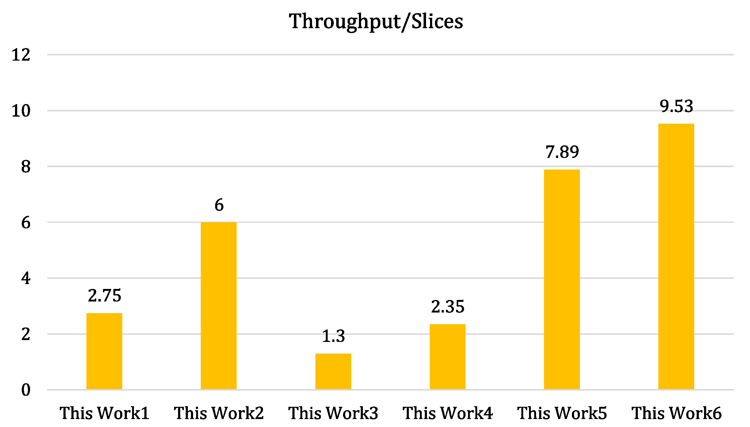
| Implemented Multiplier | Slices | LUTs | FFs | Freq. (MHz) | T/Slices |
|---|---|---|---|---|---|
| Schoolbook | 553 | 1479 | 493 | 97 | 753.4 |
| 2-way-karatsuba | 1341 | 3815 | 1206 | 86 | 556.5 |
| 3-way-toomcook | 1451 | 4816 | 3444 | 94 | 850.8 |
| 4-way-toomcook | 2052 | 4825 | 4981 | 436 | 3748.6 |
| hybrid Karatsuba | 3819 | 12,942 | 465 | 231 | 60,496.0 |
| least-significant-digit-parallel | 794 | 1573 | 233 | 416 | 526,315.7 |
| Ref #. | Area Information | Timing Information | Total Power (mW) | ||||
|---|---|---|---|---|---|---|---|
| Slices | LUTs | FFs | CCs | Freq. (MHz) | Latency (s) | ||
| This Work | 12,870 | 18,420 | 6167 | 1,382,492 | 49 | 28,214.1 | 1.46 |
| This Work | 13,658 | 20,756 | 6880 | 694,844 | 57 | 12,190.2 | 1.83 |
| This Work | 13,768 | 21,757 | 9118 | 463,652 | 83 | 5586.1 | 2.57 |
| This Work | 14,369 | 21,766 | 10,655 | 351,020 | 119 | 2949.7 | 2.92 |
| This Work | 8498 | 3999 | 5209 | 13,124 | 88 | 149.1 | 3.31 |
| This Work | 13,111 | 18,514 | 5907 | 13,124 | 164 | 80.0 | 3.16 |
| Ref #. | IMM | Device | Area Information | Timing Information | ||||
|---|---|---|---|---|---|---|---|---|
| Slices | LUTs | FFs | CCs | Freq. (MHz) | Latency (s) | |||
| [14] | 2013 | Virtex 7 | 6032 | – | – | 7370 | 183 | 40 |
| [13] | 2011 | Virtex 4 | 20,437 | – | – | 5913 | 81 | 73 |
| [17] | 2013 | Virtex 4 | 17,393 | – | – | 12,553 | 162 | 77 |
| Virtex 7 | 6342 | – | – | 12,553 | 369 | 34 | ||
| [18] | 2013 | Virtex 7 | 6083 | 22,254 | 4927 | 12,553 | 341 | 36 |
| 8866 | 23,017 | 4414 | 12,553 | 271 | 46 | |||
| [19] | 2013 | Virtex 7 | 7017 | – | – | 13,057 | 434 | 30 |
| [20] | 2018 | Virtex 7 | 7123 | – | – | 15,495 | 188 | 82.4 |
| This work | 2018 | Virtex 4 | 13,635 | 15,545 | 15,042 | 13,124 | 118 | 111 |
| This work | 2018 | Virtex 7 | 3948 | 12,652 | 6456 | 13,124 | 223 | 58 |
Publisher’s Note: MDPI stays neutral with regard to jurisdictional claims in published maps and institutional affiliations. |
© 2022 by the authors. Licensee MDPI, Basel, Switzerland. This article is an open access article distributed under the terms and conditions of the Creative Commons Attribution (CC BY) license (https://creativecommons.org/licenses/by/4.0/).
Share and Cite
Umer, U.; Rashid, M.; Alharbi, A.R.; Alhomoud, A.; Kumar, H.; Jafri, A.R. An Efficient Crypto Processor Architecture for Side-Channel Resistant Binary Huff Curves on FPGA. Electronics 2022, 11, 1131. https://doi.org/10.3390/electronics11071131
Umer U, Rashid M, Alharbi AR, Alhomoud A, Kumar H, Jafri AR. An Efficient Crypto Processor Architecture for Side-Channel Resistant Binary Huff Curves on FPGA. Electronics. 2022; 11(7):1131. https://doi.org/10.3390/electronics11071131
Chicago/Turabian StyleUmer, Usama, Muhammad Rashid, Adel R. Alharbi, Ahmed Alhomoud, Harish Kumar, and Atif Raza Jafri. 2022. "An Efficient Crypto Processor Architecture for Side-Channel Resistant Binary Huff Curves on FPGA" Electronics 11, no. 7: 1131. https://doi.org/10.3390/electronics11071131
APA StyleUmer, U., Rashid, M., Alharbi, A. R., Alhomoud, A., Kumar, H., & Jafri, A. R. (2022). An Efficient Crypto Processor Architecture for Side-Channel Resistant Binary Huff Curves on FPGA. Electronics, 11(7), 1131. https://doi.org/10.3390/electronics11071131