
Semiconducting Polymer Nanowires with Highly Aligned Molecules for Polymer Field Effect Transistors


Abstract
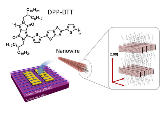
:
1. Introduction
2. Materials and Methods
2.1. Preparation of PDMS Stamps
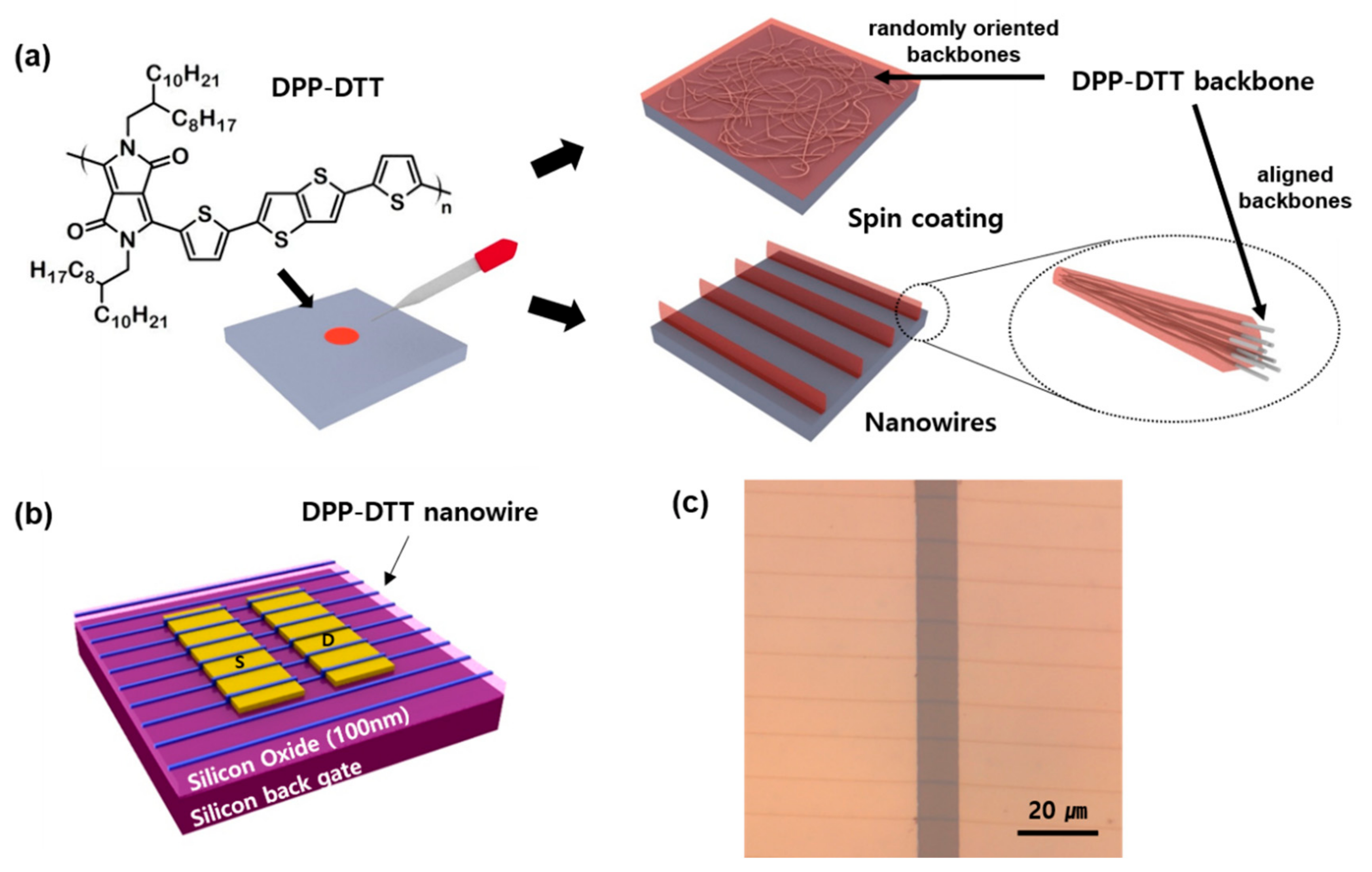
2.2. Fabrication of Polymer Nanowires
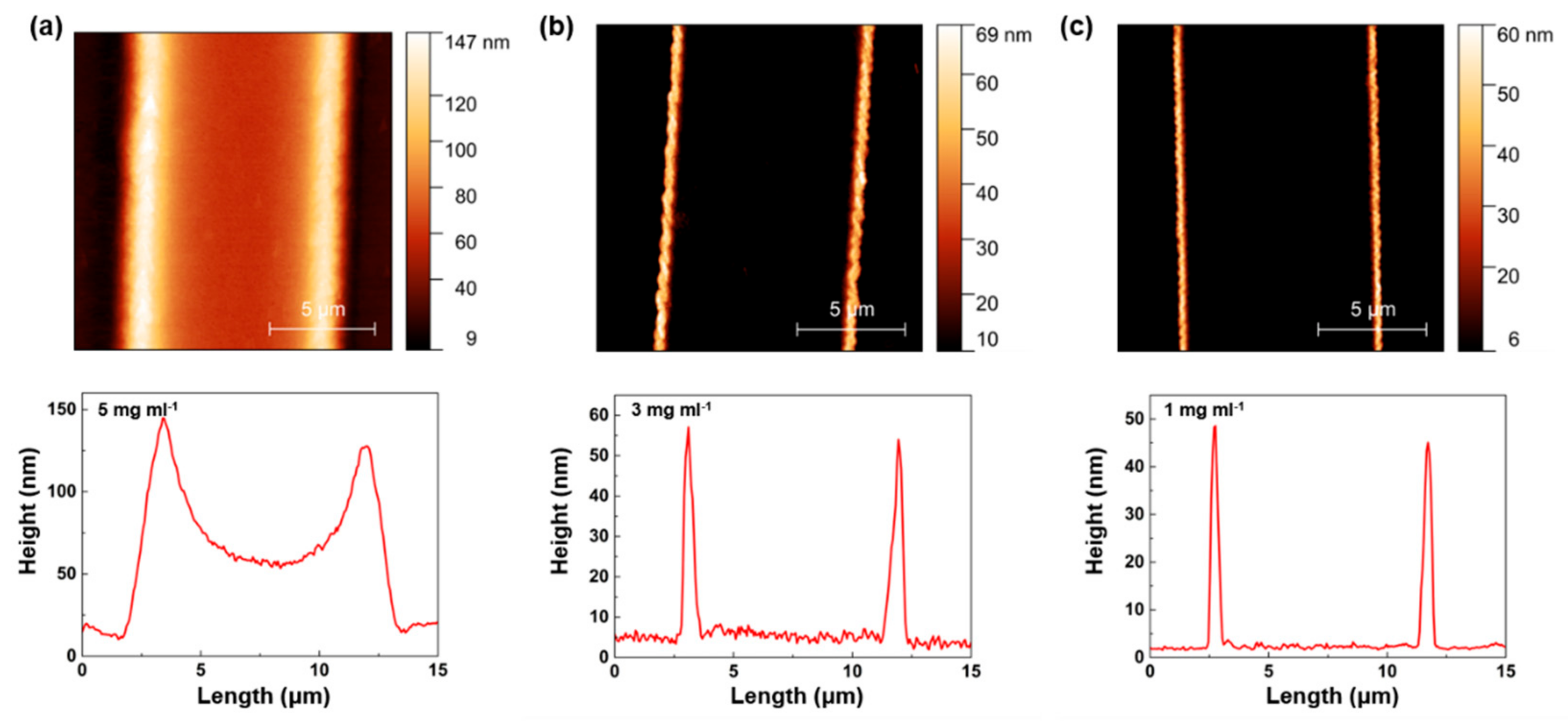
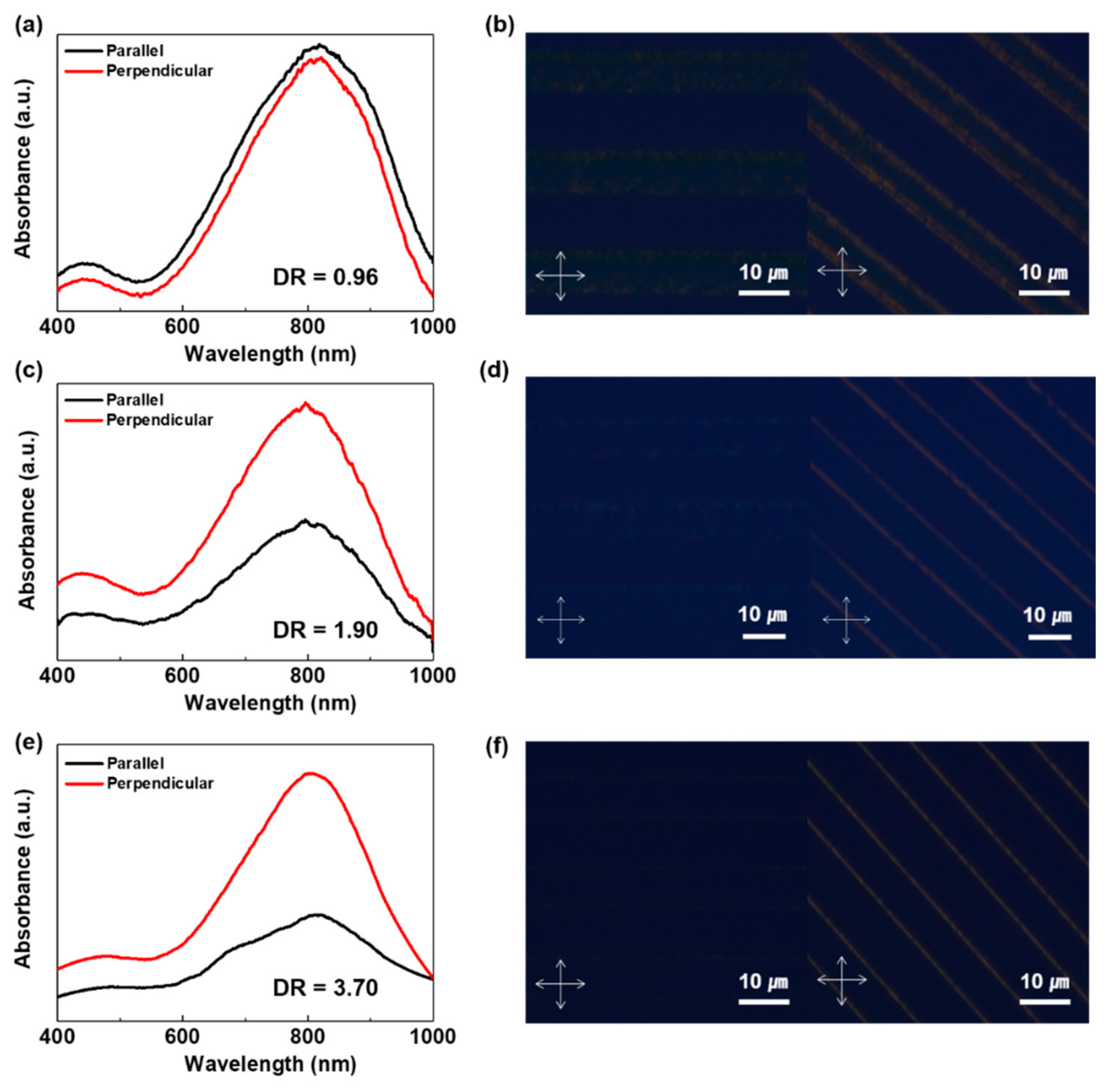
2.3. Optical and Structural Characterization
2.4. Electrical Characterization
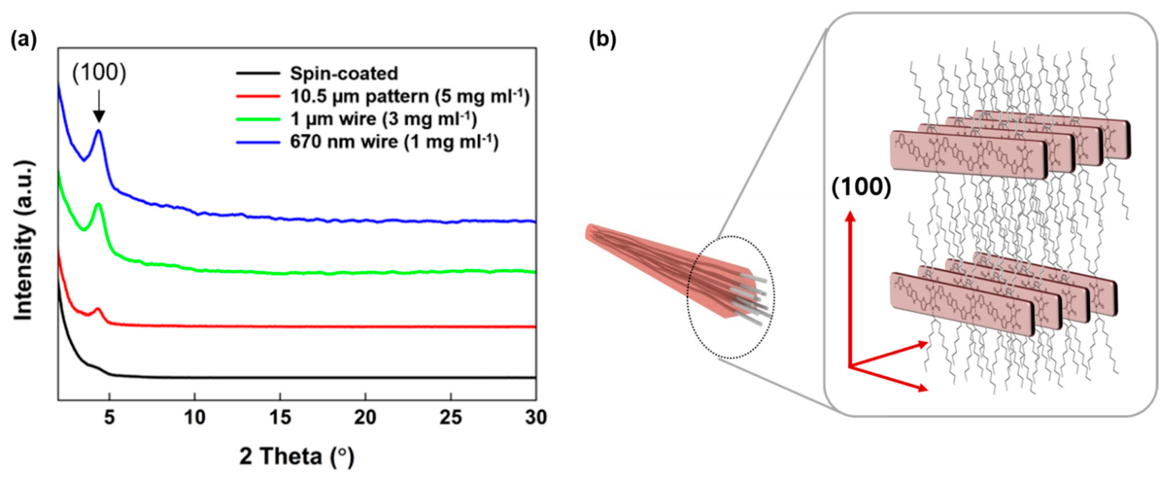
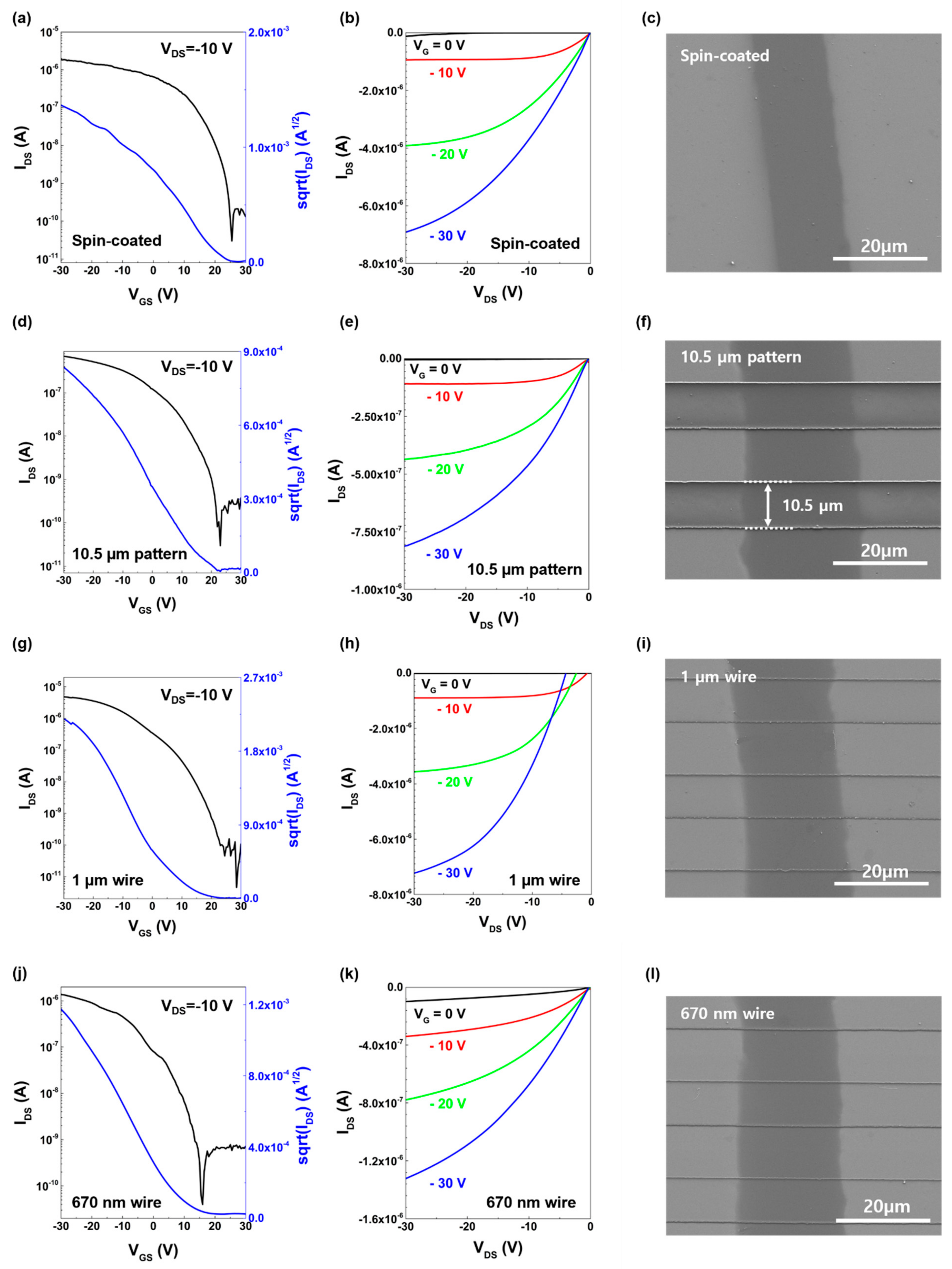
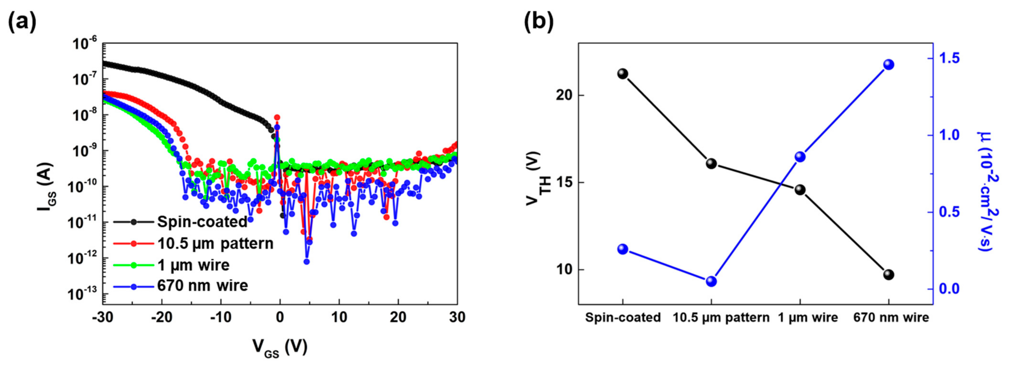
3. Results and Discussion
4. Conclusions
Author Contributions
Funding
Data Availability Statement
Conflicts of Interest
References
- Drury, C.J.; Mutsaers, C.M.J.; Hart, C.M.; Matters, M.; De Leeuw, D.M. Low-Cost All-Polymer Integrated Circuits. Appl. Phys. Lett. 1998, 73, 108–110. [Google Scholar] [CrossRef]
- Janoschka, T.; Martin, N.; Martin, U.; Friebe, C.; Morgenstern, S.; Hiller, H.; Hager, M.D.; Schubert, U.S. An Aqueous, Polymer-Based Redox-Flow Battery Using Non-Corrosive, Safe, and Low-Cost Materials. Nature 2015, 527, 78–81. [Google Scholar] [CrossRef]
- Zhang, R.; Moon, K.S.; Lin, W.; Agar, J.C.; Wong, C.P. A Simple, Low-Cost Approach to Prepare Flexible Highly Conductive Polymer Composites by in Situ Reduction of Silver Carboxylate for Flexible Electronic Applications. Compos. Sci. Technol. 2011, 71, 528–534. [Google Scholar] [CrossRef]
- Gao, H.; Li, J.; Zhang, F.; Liu, Y.; Leng, J. The Research Status and Challenges of Shape Memory Polymer-Based Flexible Electronics. Mater. Horiz. 2019, 6, 931–944. [Google Scholar] [CrossRef]
- Zardetto, V.; Brown, T.M.; Reale, A.; Di Carlo, A. Substrates for Flexible Electronics: A Practical Investigation on the Electrical, Film Flexibility, Optical, Temperature, and Solvent Resistance Properties. J. Polym. Sci. Part B Polym. Phys. 2011, 49, 638–648. [Google Scholar] [CrossRef]
- Søndergaard, R.R.; Hösel, M.; Espinosa, N.; Jørgensen, M.; Krebs, F.C. Practical Evaluation of Organic Polymer Thermoelectrics by Large-Area R2R Processing on Flexible Substrates. Energy Sci. Eng. 2013, 1, 81–88. [Google Scholar] [CrossRef] [Green Version]
- Sun, C.; Pan, F.; Bin, H.; Zhang, J.; Xue, L.; Qiu, B.; Wei, Z.; Zhang, Z.G.; Li, Y. A Low Cost and High Performance Polymer Donor Material for Polymer Solar Cells. Nat. Commun. 2018, 9, 1–10. [Google Scholar] [CrossRef]
- Tan, L.; Wang, Y.; Zhang, J.; Xiao, S.; Zhou, H.; Li, Y.; Chen, Y.; Li, Y. Highly Efficient Flexible Polymer Solar Cells with Robust Mechanical Stability. Adv. Sci. 2019, 6, 1801180. [Google Scholar] [CrossRef]
- Zheng, H.; Zheng, Y.; Liu, N.; Ai, N.; Wang, Q.; Wu, S.; Zhou, J.; Hu, D.; Yu, S.; Han, S.; et al. All-Solution Processed Polymer Light-Emitting Diode Displays. Nat. Commun. 2013, 4, 1971. [Google Scholar] [CrossRef]
- Gong, X.; Tong, M.; Xia, Y.; Cai, W.; Moon, J.S.; Cao, Y.; Yu, G.; Shieh, C.L.; Nilsson, B.; Heeger, A.J. High-Detectivity Polymer Photodetectors with Spectral Response from 300 Nm to 1450 Nm. Science 2009, 325, 1665–1667. [Google Scholar] [CrossRef]
- Boussaad, S.; Tao, N.J. Polymer Wire Chemical Sensor Using a Microfabricated Tuning Fork. Nano Lett. 2003, 3, 1173–1176. [Google Scholar] [CrossRef]
- Helgesen, M.; Søndergaard, R.; Krebs, F.C. Advanced Materials and Processes for Polymer Solar Cell Devices. J. Mater. Chem. 2010, 20, 36–60. [Google Scholar] [CrossRef]
- Wang, G.; Melkonyan, F.S.; Facchetti, A.; Marks, T.J. All-Polymer Solar Cells: Recent Progress, Challenges, and Prospects. Angew. Chem. -Int. Ed. 2019, 58, 4129–4142. [Google Scholar] [CrossRef] [PubMed]
- Liu, D.; Broer, D.J. Liquid Crystal Polymer Networks: Preparation, Properties, and Applications of Films with Patterned Molecular Alignment. Langmuir 2014, 30, 13499–13509. [Google Scholar] [CrossRef] [PubMed] [Green Version]
- Chang, M.; Choi, D.; Egap, E. Macroscopic Alignment of One-Dimensional Conjugated Polymer Nanocrystallites for High-Mobility Organic Field-Effect Transistors. ACS Appl. Mater. Interfaces 2016, 8, 13484–13491. [Google Scholar] [CrossRef] [PubMed]
- Wang, J.; Sun, X.; Chen, L.; Zhuang, L.; Chou, S.Y. Molecular Alignment in Submicron Patterned Polymer Matrix Using Nanoimprint Lithography. Appl. Phys. Lett. 2000, 77, 166–168. [Google Scholar] [CrossRef] [Green Version]
- Chang, M.; Su, Z.; Egap, E. Alignment and Charge Transport of One-Dimensional Conjugated Polymer Nanowires in Insulating Polymer Blends. Macromolecules 2016, 49, 9449–9456. [Google Scholar] [CrossRef]
- Luzio, A.; Martin, J.; Cheng, C.H.; Stingelin, N.; Toney, M.F.; Salleo, A.; Caironi, M. Improving Molecular Alignment and Charge Percolation in Semiconducting Polymer Films with Highly Localized Electronic States through Tailored Thermal Annealing. J. Mater. Chem. C 2021, 9, 15848–15857. [Google Scholar] [CrossRef]
- Khim, D.; Han, H.; Baeg, K.J.; Kim, J.; Kwak, S.W.; Kim, D.Y.; Noh, Y.Y. Simple Bar-Coating Process for Large-Area, High-Performance Organic Field-Effect Transistors and Ambipolar Complementary Integrated Circuits. Adv. Mater. 2013, 25, 4302–4308. [Google Scholar] [CrossRef]
- Lee, S.B.; Kang, B.; Kim, D.; Park, C.; Kim, S.; Lee, M.; Lee, W.B.; Cho, K. Motion-Programmed Bar-Coating Method with Controlled Gap for High-Speed Scalable Preparation of Highly Crystalline Organic Semiconductor Thin Films. ACS Appl. Mater. Interfaces 2019, 11, 47153–47161. [Google Scholar] [CrossRef]
- Yoon, D.K.; Kim, H.; Kim, B.S.; Han, M.J.; Kim, J.; Kim, B.; Park, S.M.; Ahn, H.; Shin, T.J. Orientation Control of Semiconducting Polymers Using Microchannel Molds. ACS Nano 2020, 14, 12951–12961. [Google Scholar] [CrossRef]
- Martin, C.R.; Aksay, I.A. Microchannel Molding: A Soft Lithography-Inspired Approach to Micrometer-Scale Patterning. J. Mater. Res. 2005, 20, 1995–2003. [Google Scholar] [CrossRef]
- Knobloch, A.; Bernds, A.; Clemens, W. Printed Polymer Transistors. In Proceedings of the First International IEEE Conference on Polymers and Adhesives in Microelectronics and Photonics, Incorporating POLY, PEP & Adhesives in Electronics. Proceedings (Cat. No.01TH8592), Potsdam, Germany, 21–24 October 2001; pp. 84–90. [Google Scholar]
- Balocco, C.; Majewski, L.A.; Song, A.M. Non-Destructive Patterning of Conducting-Polymer Devices Using Subtractive Photolithography. Org. Electron. 2006, 7, 500–507. [Google Scholar] [CrossRef]
- Li, S.; Chun, Y.T.; Zhao, S.; Ahn, H.; Ahn, D.; Sohn, J.I.; Xu, Y.; Shrestha, P.; Pivnenko, M.; Chu, D. High-Resolution Patterning of Solution-Processable Materials via Externally Engineered Pinning of Capillary Bridges. Nat. Commun. 2018, 9, 393. [Google Scholar] [CrossRef] [PubMed] [Green Version]
- Li, Q.Y.; Yao, Z.F.; Lu, Y.; Zhang, S.; Ahmad, Z.; Wang, J.Y.; Gu, X.; Pei, J. Achieving High Alignment of Conjugated Polymers by Controlled Dip-Coating. Adv. Electron. Mater. 2020, 6, 2000080. [Google Scholar] [CrossRef]
- Syafutra, H.; Pandey, M.; Kumari, N.; Pandey, S.S.; Benten, H.; Nakamura, M. Assisted Alignment of Conjugated Polymers in Floating Film Transfer Method Using Polymer Blend. Thin Solid Films 2021, 734, 138814. [Google Scholar] [CrossRef]
- Khim, D.; Luzio, A.; Bonacchini, G.E.; Pace, G.; Lee, M.-J.; Noh, Y.-Y.; Caironi, M. Uniaxial Alignment of Conjugated Polymer Films for High-Performance Organic Field-Effect Transistors. Adv. Mater. 2018, 30, 1705463. [Google Scholar] [CrossRef]
- Lin, F.J.; Guo, C.; Chuang, W.T.; Wang, C.L.; Wang, Q.; Liu, H.; Hsu, C.S.; Jiang, L. Directional Solution Coating by the Chinese Brush: A Facile Approach to Improving Molecular Alignment for High-Performance Polymer TFTs. Adv. Mater. 2017, 29, 1606987. [Google Scholar] [CrossRef]
- Lei, Y.; Wu, B.; Chan, W.-K.E.; Zhu, F.; Ong, B.S. Engineering Gate Dielectric Surface Properties for Enhanced Polymer Field-Effect Transistor Performance. J. Mater. Chem. C 2015, 3, 12267–12272. [Google Scholar] [CrossRef]
- Garnier, F.; Horowitz, G.; Peng, X.; Fichou, D. An All-organic “Soft” Thin Film Transistor with Very High Carrier Mobility. Adv. Mater. 1990, 2, 592–594. [Google Scholar] [CrossRef]
- Hengen, S.; Alt, M.; Hernandez-Sosa, G.; Giehl, J.; Lemmer, U.; Mechau, N. Modelling and Simulation of Gate Leakage Currents of Solution-Processed OTFT. Org. Electron. 2014, 15, 829–834. [Google Scholar] [CrossRef]
- Kehrer, L.A.; Winter, S.; Fischer, R.; Melzer, C.; Von Seggern, H. Temporal and Thermal Properties of Optically Induced Instabilities in P3HT Field-Effect Transistors. Synth. Met. 2012, 161, 2558–2561. [Google Scholar] [CrossRef]
- Zessin, J.; Xu, Z.; Shin, N.; Hambsch, M.; Mannsfeld, S.C.B. Threshold Voltage Control in Organic Field-Effect Transistors by Surface Doping with a Fluorinated Alkylsilane. ACS Appl. Mater. Interfaces 2019, 11, 2177–2188. [Google Scholar] [CrossRef] [PubMed]

| Threshold Voltage, VTH (V) | Mobility, μ (cm2 V−1 s−1) | On/Off Current Ratio | Gate Leakage Current, IGS (A) | |
|---|---|---|---|---|
| Spin-coated | 21.24 | 0.26 × 10⁻² | ~104 | 10−9~10−6 |
| 10.5 μm patterns (5 mg mL−1) | 16.08 | 0.05 × 10⁻² | ~104 | 10−10~10−7 |
| 1 μm wires (3 mg mL−1) | 14.58 | 0.86 × 10⁻² | ~105 | 10−10~10−7 |
| 670 nm wires (1 mg mL−1) | 9.71 | 1.46 × 10⁻² | ~105 | 10−11~10−7 |
Publisher’s Note: MDPI stays neutral with regard to jurisdictional claims in published maps and institutional affiliations. |
© 2022 by the authors. Licensee MDPI, Basel, Switzerland. This article is an open access article distributed under the terms and conditions of the Creative Commons Attribution (CC BY) license (https://creativecommons.org/licenses/by/4.0/).
Share and Cite
Park, K.J.; Kim, C.W.; Sung, M.J.; Lee, J.; Chun, Y.T. Semiconducting Polymer Nanowires with Highly Aligned Molecules for Polymer Field Effect Transistors. Electronics 2022, 11, 648. https://doi.org/10.3390/electronics11040648
Park KJ, Kim CW, Sung MJ, Lee J, Chun YT. Semiconducting Polymer Nanowires with Highly Aligned Molecules for Polymer Field Effect Transistors. Electronics. 2022; 11(4):648. https://doi.org/10.3390/electronics11040648
Chicago/Turabian StylePark, Keon Joo, Chae Won Kim, Min Jae Sung, Jiyoul Lee, and Young Tea Chun. 2022. "Semiconducting Polymer Nanowires with Highly Aligned Molecules for Polymer Field Effect Transistors" Electronics 11, no. 4: 648. https://doi.org/10.3390/electronics11040648
APA StylePark, K. J., Kim, C. W., Sung, M. J., Lee, J., & Chun, Y. T. (2022). Semiconducting Polymer Nanowires with Highly Aligned Molecules for Polymer Field Effect Transistors. Electronics, 11(4), 648. https://doi.org/10.3390/electronics11040648