Review

Ferroelectrics Based on HfO2 Film

by
Chong-Myeong Song
1 and
Hyuk-Jun Kwon
1,2,*
1
Department of Information and Communication Engineering, Daegu Gyeongbuk Institute of Science and Technology (DGIST), Daegu 42988, Korea
2
Convergence Research Advanced Centre for Olfaction, Daegu Gyeongbuk Institute of Science and Technology (DGIST), Daegu 42988, Korea
*
Author to whom correspondence should be addressed.
Electronics 2021, 10(22), 2759; https://doi.org/10.3390/electronics10222759
Submission received: 19 October 2021 / Revised: 8 November 2021 / Accepted: 9 November 2021 / Published: 11 November 2021
(This article belongs to the Special Issue Applications of Thin Films in Microelectronics)

Abstract

:
The discovery of ferroelectricity in HfO2 thin film, which is compatible with the CMOS process, has revived interest in ferroelectric memory devices. HfO2 has been found to exhibit high ferroelectricity at a few nanometers thickness, and studies have rapidly progressed in the past decade. Ferroelectricity can be induced in HfO2 by various deposition methods and heat treatment processes. By combining ferroelectric materials with field-effect transistors, devices that combine logic and memory functions can be implemented. Ferroelectric HfO2-based devices show high potential, but there are some challenges to overcome in endurance and characterization. In this paper, we discuss the fabrication and characteristics of ferroelectric HfO2 film and various applications, including negative capacitance (NC)), Ferroelectric random-access memory (FeRAM), Ferroelectric tunnel junction (FTJ), and Ferroelectric Field-effect Transistor (FeFET).

1. Introduction

With the increasing demand for AI technology, driven by the development of machine learning and deep learning, demand for computing power is also increasing [1]. However, there is a bottleneck in the von Neumann architecture still widely in use today, in that data cannot be processed and read simultaneously. This is due to the structure, where the storage space and computational space are separated. This bottleneck leads to low energy efficiency when processing large amounts of data. As an alternative to the von Neuman computer architecture, non-volatile memory (NVM) has been attracting attention, offering high energy efficiency, high densities, and merged logic-memory functionality. In addition, ferroelectrics are expected to be used as next-generation NVM devices because of their physical properties. Ferroelectric materials have two different remanent polarization states without an external electric field below the Curie temperature [2]. By taking advantage of these characteristics, a memory device can be made with a one transistor-one capacitor (1T-1C) structure that behaves like a 6T-SRAM, resulting in higher density [3,4]. Furthermore, ferroelectric devices can change their polarization state using voltage pulses to create multi-level current states, making them suitable for neuromorphic devices [5,6].
In the early days, ferroelectric devices were developed using perovskite materials such as Pb (Zr, Ti) O3 (PZT), BaTiO3 (BTO), and SrBi2Ta2O9 (SBT) [7,8]. However, to exhibit ferroelectricity, these perovskite materials require a relatively thick film (TFE > 100 nm) and have a relatively small energy bandgap of 3–4 eV, which is vulnerable to leakage current and electrical breakdown [8,9]. After the ferroelectric properties of Si-doped HfO2 thin films (which have excellent ferroelectricity even at thicknesses below 10 nm and a relatively large energy bandgap (Eg~5.7 eV)) were reported in 2011, many studies have actively reported using them [10,11]. HfO2 has already been used in high-k metal gate (HKMG) technology for logic transistors, and its compatibility and scalability with CMOS technology have supported its potential for ferroelectric devices in mass-produced semiconductor components. Accordingly, ferroelectric HfO2 based devices have been studied in various fields of application, including next-generation memory devices and logic devices such as FRAM [12,13,14], FTJ [15,16,17,18,19], and FeFET [20,21,22].
This review paper mainly discusses key points about the fabrication and applications of ferroelectric HfO2 films. For this purpose, in Section 2, we introduce the various deposition methods and annealing processes for fabricating ferroelectric HfO2 film. In Section 3, we present various measurements for analyzing ferroelectric HfO2 film. In Section 4, we will review the most representative application devices using ferroelectric HfO2 film: negative capacitance (NC), Ferroelectric random-access memory (FeRAM), Ferroelectric tunnel junction (FTJ), and Ferroelectric Field-effect Transistor (FeFET). We conclude in Section 5.

2. Fabrication of Ferroelectric HfO2 Film

Depending on process conditions, the properties of ferroelectric HfO2 film will differ, and this allows diverse device applications. The ferroelectricity in HfO2 arises from the metastable orthorhombic phase, which depends on the deposition method and heat treatment process. The metastable orthorhombic phase is typically generated from five roots: doping, oxygen vacancy, surface/interface/grain boundary energy, electrical field, and stress [23]. This makes it important to analyze the principles of deposition and heat treatment techniques to understand the HfO2 film. Deposition methods include atomic layer deposition (ALD—Section 2.1), physical vapor deposition (PVD—Section 2.2), pulsed laser deposition (PLD—Section 2.3), and chemical solution deposition (CSD—Section 2.3). Ferroelectricity is generally induced by the rapid thermal annealing (RTA) process and other heat sources after deposition (Section 2.4).

2.1. Atomic Layer Deposition (ALD)

ALD is a self-limiting growth method which forms a thin film based on the chemical reaction of a precursor and reactant molecules on the surface [24]. Because the atomic thickness can be precisely controlled, this provides advantages for three-dimensional (3D) structures in semiconductor device fabrication [21,25]. HfO2 films are also used in HKMG technology with mature ALD technology due to their high-k feature and low leakage current.
Various Hf precursors and oxygen sources, such as H2O, O2 plasma, and ozone are used for deposition of HfO2 film using ALD. In the case of an Hf Chloride precursor (HfCl4), high-temperature thermal ALD is possible due to its thermal stability, but corrosive by-products such as HCL and chlorine contamination can be induced. Cyclopentadienyl Hf precursors (Cp2HfMe2, (MeCp)2HfMe2, and (MeCp)2Hf(OMe)Me) have promising characteristics with good thermal stability and low impurity contamination, but the growth rate from cyclopentadienyl Hf precursors is lower than other Hf precursors. In general, alkylamides (e.g., alkoxide precursors (Hf(NetMe)4 and HF(NMe2)4)) show limited thermal stability of up to 250–300 °C, but show desirable properties with low impurity contamination and dense film, and thus are widely used to grow HfO2 films using thermal ALD and PEALD. In this respect, for tuning high-quality HfO2 films, precursor design and a well-established procedure are considered in the ALD process.
These HfO2 films have various phases: centrosymmetric structures (monoclinic (m-phase), tetragonal (t-phase), cubic (c-phase)) and a non-centrosymmetric structure (orthorhombic phase (o-phase)). In the centrosymmetric structures, the HfO2 film has dielectric properties, but when proper doping and annealing are used for the o-phase, it achieves a non-centrosymmetric meta-stable state and has ferroelectric properties [10] (Figure 1a). For example, dopants with various atomic radius can affect the bonding of metals and oxygen to induce a ferroelectric o-phase. Therefore, doping can help suppress monoclinic phase formation, which makes it difficult to transit to other phases of HfO2. In addition, the doping concentration should be sufficient to suppress the formation of monoclinic phases during the annealing process for crystallization. Too high doping concentrations make transition temperature and transition reaction to the orthorhombic phase difficult.
Various dopants such as Si, Al, Y, Gd, La, and Sr are used to induce ferroelectricity in ferroelectric HfO2 with ALD (Figure 1b) [26]. Groups below the crystal radius of Hf (<155 pm) (e.g., Si, Al, Zr) stabilize in the t-phase, and groups above the crystal radius of Hf (>155 pm) (e.g., Y, Gd, La, Sr) stabilize in the c-phase. HfO2, which has various phases depending on these dopants, becomes o-phase with ferroelectricity through an appropriate annealing process. (More details on the annealing process will be discussed in Section 2.4 below). Polarization of up to 50 μC/cm2 can be induced in these doped ferroelectric HfO2 films, and there is a suitable concentration range of dopants to form o-phases [27].
It has also been reported that the doping induced ferroelectricity of HfO2 can be increased more than tenfold when integrated into a 3D structure using ALD [25]. In addition, high density memory can be achieved with a 3D architecture and vertical integration because ALD provides excellent step coverage, in order to obtain uniform HfO2 thin film with a high aspect ratio structure compared to other PVD and CVD methods. However, ferroelectric HfO2 films made by ALD are polycrystalline and therefore have various non-ferroelectric phases [28,29].
In addition, it is difficult to achieve uniform ferroelectricity in very thin film. The disordered and polycrystalline oxide film causes various problems, with changing threshold voltage as well as the non-uniform doping [30]. These problems are challenges that remain to be solved by optimization of deposition techniques and by understanding ferroelectric mechanisms in HfO2 film.
Figure 1. (a) A qualitative model of film conditions, crystal, and thermal budget [31] Copyright 2015, AIP Publishing LLC. (b) Remnant polarization of ferroelectric HfO2 film as a function of dopant content and doping concentration. Reproduced with permission [23]. Copyright 2019, Elsevier Ltd.
Electronics 10 02759 g001

2.2. Sputtering

Sputtering is one of the PVD methods and forms a thin film by ejecting atoms from a target as accelerated plasma to collide at low pressure with a substrate. Unlike ALD, which has fewer deposition parameters, sputtering power, and atmosphere can be easily controlled, and thus it is widely used in research for forming ferroelectric HfO2 [24,32]. Olsen et al. first reported the ferroelectricity of sputtered HfO2 film by controlling the doping concentration of yttrium through the sputtering power of the Y2O3 target [33], and then Xu et al. induced ferroelectricity in HfO2 thin films by doping cations (e.g., Sc, Ge, Y, Zr, Nb) or an anion (N) at various doping concentrations by controlling sputter power [34]. Furthermore, it was reported that ferroelectric properties can be obtained from undoped HfO2 films by controlling oxygen flow during sputter deposition [35].
Sputtering has the advantages of high deposition rate due to the low-pressure deposition process, and having less binding to impure materials, such as C, N, or H, which affect the quality and polymorphism of the ferroelectric HfO2 thin films [36,37]. In addition, since the film can be grown at room temperature, it is expected to allow ferroelectric devices to be manufactured on flexible substrates with low thermal resistance [38,39]. However, high energy deposition can cause damage, and compared to ALD, it is more difficult to fabricate a 3D structure, and the many conditions used in deposition can be factors that make it difficult for various applications.

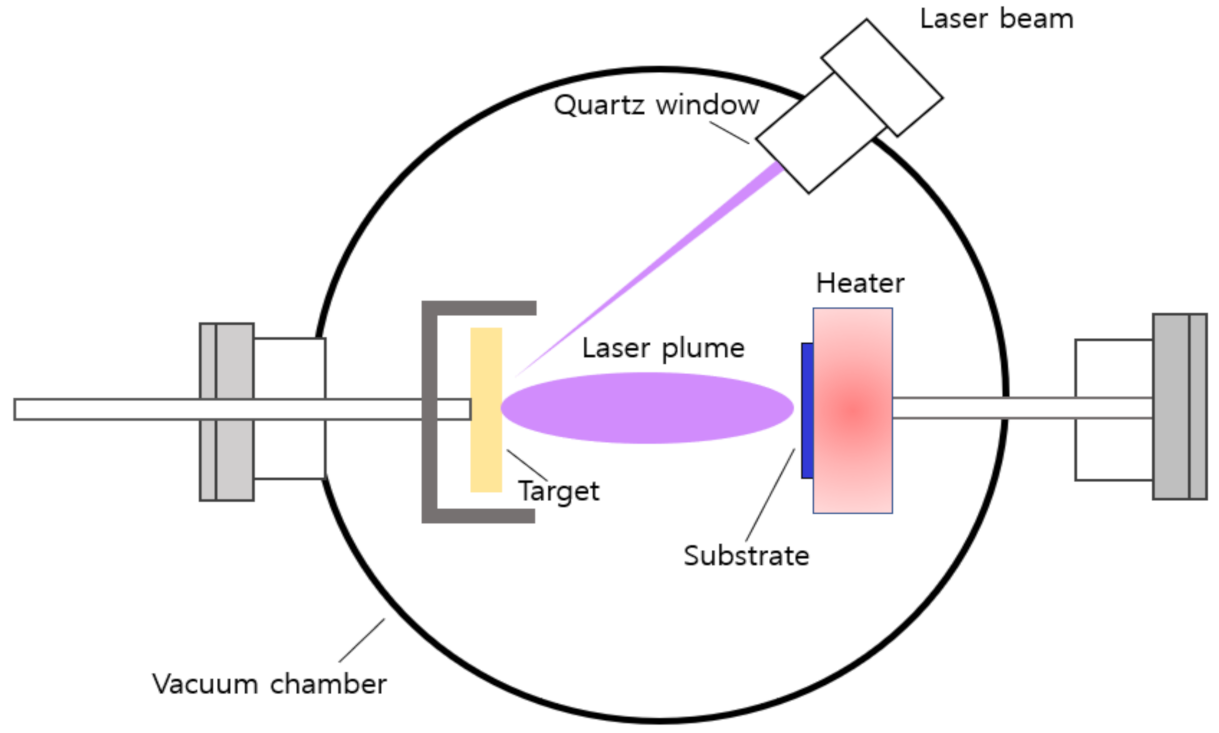
2.3. Pulsed Laser Deposition (PLD)

PLD is a method of forming a thin film by irradiating a strong pulsed laser beam onto a target, breaking the bonds of the target sample [40]. The plume generated by the reaction between the laser and the target reaches the surface of the substrate and forms a thin film (Figure 2). In general, PLD uses a KrF excimer laser with a wavelength of 248 nm and repetition rate of about several Hz. The thickness of the thin film can be controlled by the number of times the laser irradiation is repeated, and films with various crystallinity, from amorphous to polycrystalline, can be grown by controlling the conditions of the chamber and substrate. In particular, it is possible to form an epitaxial HfO2 film using PLD, which is the basis of research to understand the physical and structural properties of the grown ferroelectric HfO2 interface and crystal structure.
By providing nuclei with an appropriate lattice constant, such as yttria-stabilized zirconia (YSZ) and lanthanum strontium manganese oxide (LSMO), the epitaxial thin film HfO2 can be grown with an almost uniform direction under the environment of 600–1000 °C using heater and appropriate oxygen partial pressure in the chamber. By studying MFM structures with PLD-fabricated epitaxial HfO2, it was found that epitaxial HfO2 film has strong endurance, able to withstand 5 MV/cm, while Ec was 3–4 MV/cm [41,42]. While PLD has shortcomings, in that large-area deposition, it is difficult and particulates can occur, it also has the advantage of fabricating epitaxial thin film simply with various compositions. Therefore, using PLD can greatly contribute to understanding the structural and physical properties of HfO2. In addition, it is expected that fabricating devices based on epitaxial HfO2 will further understanding of ferroelectric HfO2 [16,43,44].

2.4. Chemical Solution Deposition (CSD)

CSD is a method of making oxide films through pyrolysis and the crystallization of precursors. Functional oxide films can be made using two pathways: sol-gel and metalloorganic deposition (MOD). The sol-gel method makes an oxide film with metal alkaline oxide using a hydrolysis and condensation process [45]. MOD is a method of making an oxide film without a condensation process after deposition using carboxylate and acetylacetonate educt [46].
Solutions dispensed via these two routes can be used to form an oxide thin film on the substrate by various coating methods (e.g., dip coating, spin coating, and spray coating) and can be prepared with various ratios of composition and dopant concentration [47,48,49,50,51,52,53,54,55,56,57,58,59]. Figure 3a shows a schematic of the workflow for preparing a sample by CSD. The solution dispensed on the substrate is subsequently thermal treated to crystallize it, by the evaporation of solvent and decomposition of the organic residues. When a ferroelectric HfO2 thin film was formed using Yttrium as a dopant with CSD, the Yttrium doping showed the highest remanent polarization, and the remanent polarization gradually decreased based on ionic radius, from the point showing the maximum polarization (Figure 3b) [55,56].
Ferroelectric HfO2 film made by CSD can be applied to NCFETs with improved on/off ratio and subthreshold swing (SS), demonstrating the potential of using solution processes to apply ferroelectric HfO2 to electronic devices [49,51,54]. However, compared to other deposition methods, it is not to precisely control the thin film and have good performance, but if a stable and homogeneous precursor solution can be produced through appropriate material selection, it is expected that rapid and simple deposition and environment-friendly device production will be possible [60].

2.5. Thermal Annealing

Most of the deposited HfO2 films have crystal seeds with an amorphous form of 2–3 nm diameter, and an annealing process is essential to induce a ferroelectric orthorhombic phase. Thermal annealing makes HfO2 film have thermodynamic stability at various temperatures in various phases. During the high-temperature annealing process, amorphous films are crystallized into various crystalline phases, transferring to monoclinic, tetragonal, and orthorhombic phases. In the process of thermal annealing, the crystallized film can be transformed into a ferroelectric orthorhombic phase.
Various annealing process can be used to induce ferroelectricity in HfO2 including RTA [58,61,62], furnace [49,63], hot plate [64], flash lamp [65], and laser [66,67] techniques. Among them, RTA is the most commonly used method for the crystallization of ferroelectric HfO2, and post-deposition annealing (PDA) and post-metallization annealing (PMA) can be used. Here, we note that PDA refers to a method of performing RTA without a TiN capping layer, and PMA refers to a method of performing RTA after depositing a TiN capping layer. The characteristics of HfO2 can also vary depending on the gas partial pressure, temperature rise rate, and annealing duration [58,61,62]. While a crystallization process through heat treatment is essential to induce ferroelectricity in HfO2, such heat treatment processes require a high temperature environment, and thus it is difficult to use with flexible substrates having low thermal resistance.
Because of this, studies on the formation of ferroelectric HfO2 thin film on PI films have reported poor physical and ferroelectric properties [64,68]. Recently, a mica substrate with high thermal resistance was used for flexible ferroelectric HfO2 film but had a problem with poor versatility [69]. Therefore, to employ ferroelectric HfO2 on a flexible device, it will be necessary to introduce a fundamentally low-temperature process. If new heat treatment methods, such as DUV irradiation (Figure 4a) [70], flash lamp [65], laser (Figure 4b) [66,67], etc., can be applied for low temperature processing, or the existing RTA technology can be made applicable at low temperature [71,72,73], it would open the door for ferroelectric HfO2-based flexible devices.

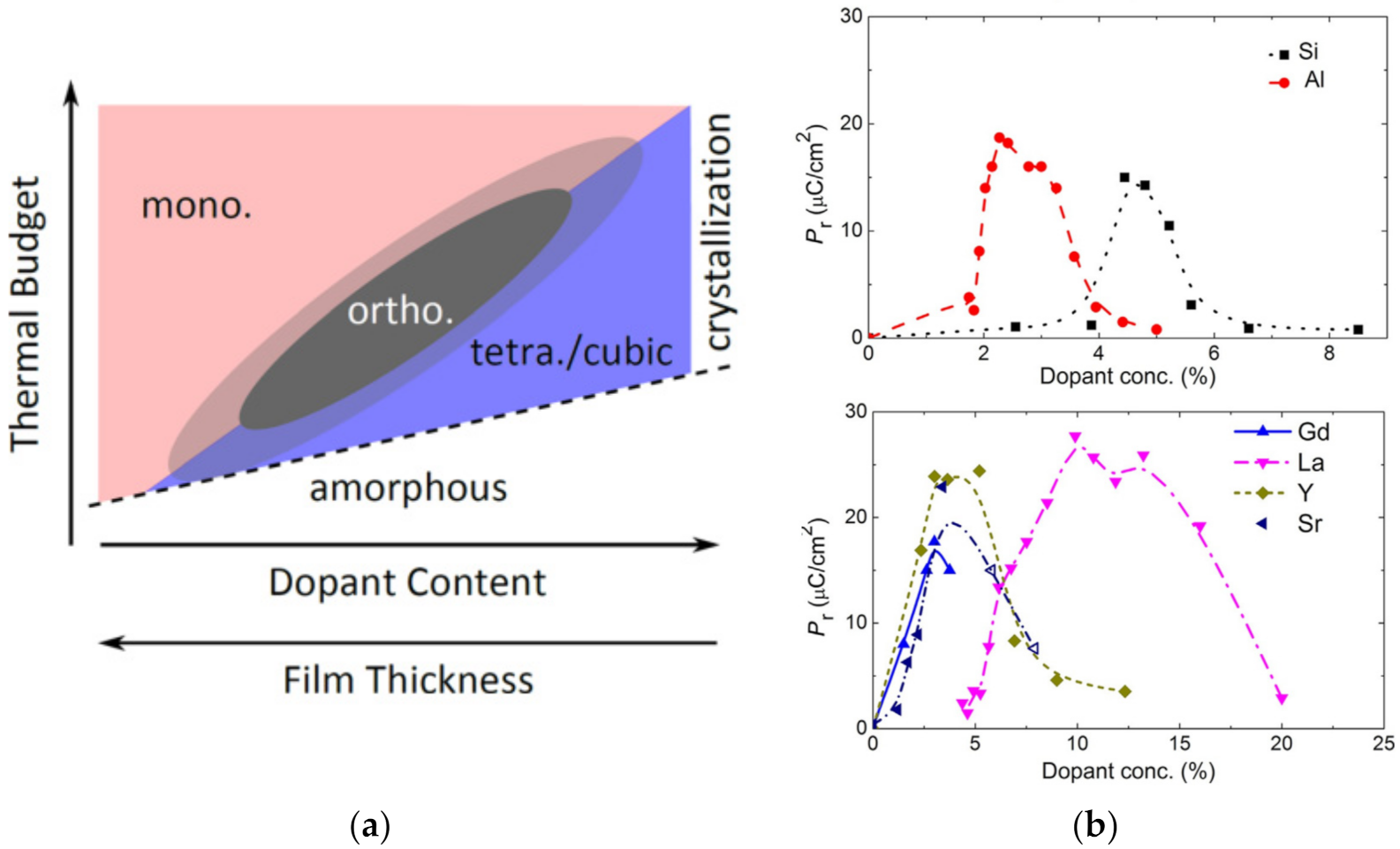
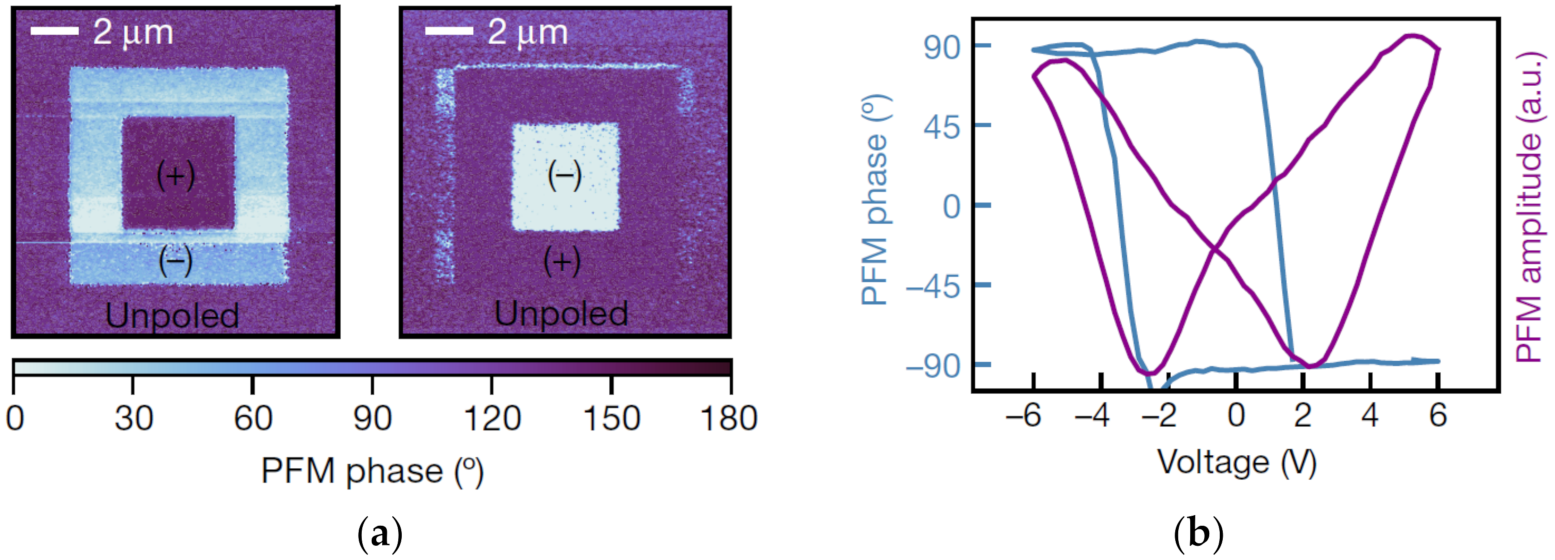
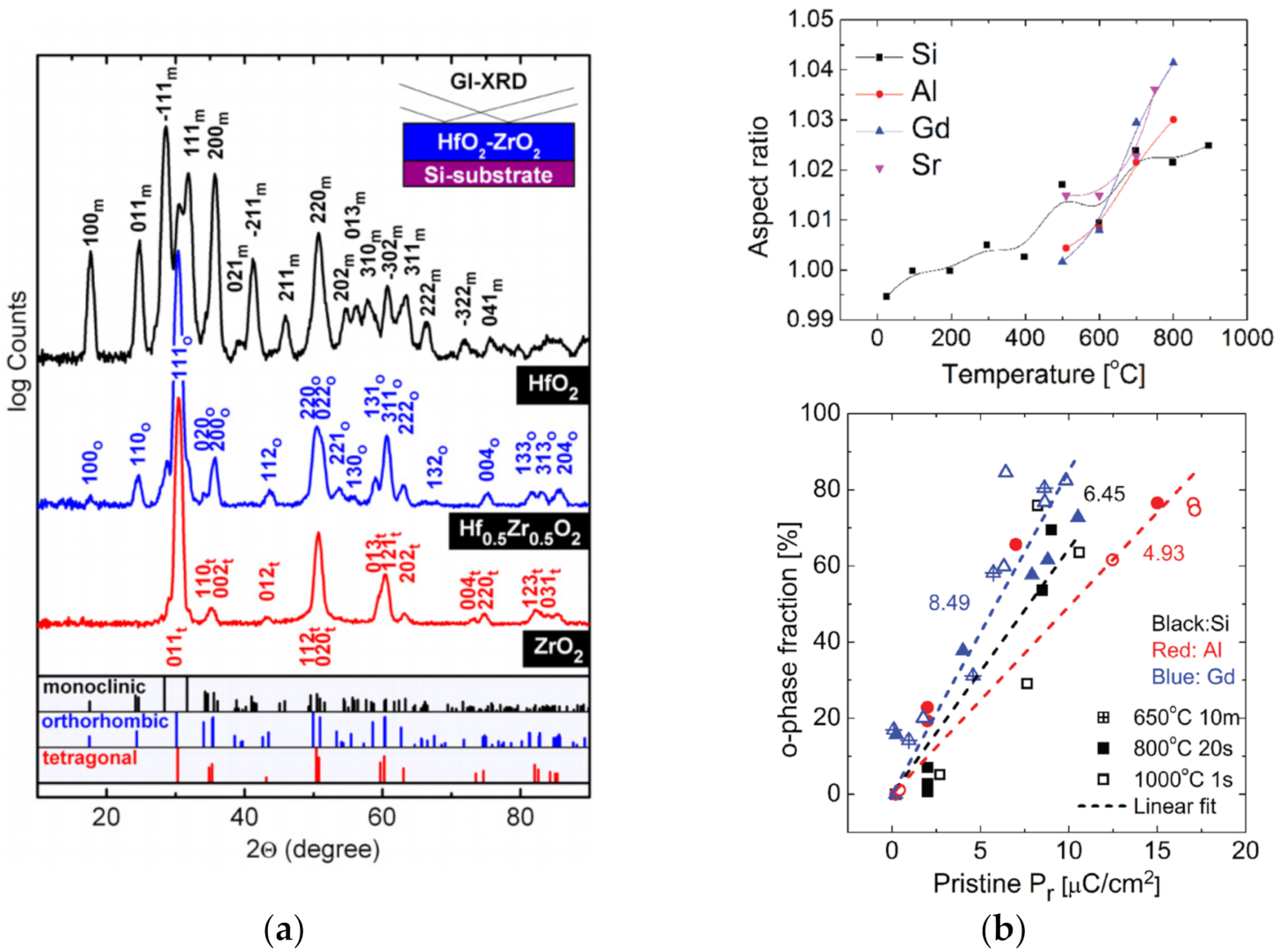
3. Analysis of Ferroelectric HfO2 Film

The P–V measurement is a representative method for confirming the presence of ferroelectricity and measuring the degree of polarization of a sample. Two types of stable polarization can be formed by domains using an external applied voltage, and physical switching variables such as remnant polarization (Pr) and coercive field (Ec) can be extracted from the measured P–V hysteresis curve [10,26,74]. However, in a film that is too thin, where the leakage current is greater than the polarization switching current, it is difficult to observe ferroelectricity in the thin film. In this case, the non-ferroelectric properties can be removed using the PUND method to extract the remnant polarization (Figure 5a) [75]. The PUND method measures polarization in the up state by applying two positive bias pulses and then two negative pulses to measure polarization in the down state (Figure 5b). The first positive pulse creates the polarization of the up state and the relaxed charge can be measured through the next positive pulse. After measuring with two positive pulses, the polarization of the down state is measured using two negative pulses.
Using the P–V measurement method, macroscopic switching characteristics can be measured, but the switching characteristics of nanoscale or local areas are difficult to measure. Piezoelectric force microscopy (PFM) can observe the changing piezoelectric effect on the surface by applying a single frequency AC field below the contact resistance frequency to the atomic force microscopy (AFM) tip. This is a way to measure microscopic polarization [26,67,76]; as shown in Figure 6, and a mixture of surface topography, amplitude, and phase can be obtained [77].
In addition to these electrical properties, structurally the ferroelectricity of HfO2 has its origin in the orthorhombic phase, which is a non-centrosymmetric structure. The peak (o-111) of the orthorhombic phase (about 2θ = 30.4°) can be checked with grazing incidence X-ray diffraction (GI-XRD), and the ferroelectricity of the HfO2 can also be confirmed by structural analysis (Figure 7a). Although the O-phase peak is difficult to distinguish from the Tetragonal peak, since ferro-genetic properties do not appear in the central symmetrical structure, an orthorhombic peak can be confirmed by comparing with the P–V characteristics. In addition to this analysis, XRD is a general technique for observing the structural properties of ferroelectric HfO2 thin films (such as aspect ratio, unit cell volume, phase ratio, and pristine Pr, etc.) (Figure 7b) [10,31,74,78,79].
STEM analysis helps to intuitively confirm the phase, phase transition, surface, thickness, and continuity of the ferroelectric HfO2 thin film [29,80,81]. Sang et al. directly confirmed the presence of an orthorhombic phase in a ferroelectric HfO2 thin film using STEM [81]. Furthermore, using STEM, it was found that abundant oxygen vacancies induce hysteresis pinching in non-uniform interfacial layers [29,80]. By redistributing the oxygen vacancies of a non-uniform interface through wake-up cycling, the internal bias fields can be reduced and the thin film can be made uniform. In addition, it was possible to directly observe the change from the m-phase to the o-phase at the interface during wake-up cycling using STEM (Figure 8) [80].

4. Application of Ferroelectric HfO2 Film

In this section, negative capacitor and memory devices such as FeRAM, FeFET, and FTJ using the aforementioned various characteristics of ferroelectric HfO2 are introduced. The NC characteristic of NCFETs can be used, where the ferroelectric layer is stacked for the gate insulating film of the FET in CMOS logic devices, and utilized for low power and fast device implementation (Section 4.1).
In addition, it is expected that polarization switching in the ferroelectric layer by external voltage can be used for ferroelectric memory, to store information in a low power and fast memory device, to replace the currently used DRAM or flash memory. Information about various ferroelectric memories is summarized in Table 1 below.
FeRAM has a 1T–1F structure and has destructive characteristics in the read process, but it can read and write faster than other NVM devices (Section 4.2). FTJ is a ferroelectric memory based on a change in resistance due to a change in tunneling barrier when switching the polarization state in an MFM structure (Section 4.3). Due to its non-destructive characteristics and simple structure, a high-density memory can be implemented, but there is a problem with endurance due to tunneling current.
Finally, FeFET, introduced in Section 4.4, combines a ferroelectric layer into the gate stack, so it can achieve higher integration than FeRAM in a device that functions as a memory through a change in threshold voltage, like a flash memory. The discovery of ferroelectricity in HfO2 thin films with non-volatile properties, suitable for such CMOS processes, has not only revived interest in non-volatile memory, but is also attracting attention as a powerful next-generation memory device.

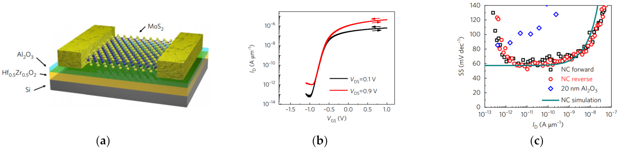
4.1. Negative Capacitance (NC)

The very important discovery of NC in ferroelectric thin films can enable the realization of low-power CMOS logic devices, by exploiting the NC effect in ferroelectric gate FETs. The NC effect in ferroelectric materials occurs when the polarization state is changed by an external electric field passing through the NC region. The Landau–Ginzburg–Devonshire approach is the model for understanding this thermodynamic property in a ferroelectric material, and predicting NC. To explain the thermodynamic properties of ferroelectrics, Devonshire introduced a phase transformation thermodynamic equation based on Landau’s symmetry [83]. In particular, the Landau–Ginzburg equation was proposed by Ginzburg to express the thermodynamic state of a finite system such as a thin film, and the following Ginzburg–Devonshire equation is currently used to simulate the thermodynamic state of a ferroelectric thin film:
α P + β P 3 + δ P 5 ξ 2 P z 2 η 2 P x 2 + 2 P y 2 = φ z
The Landau–Khalatnikov equation is a brief representation of a one-dimensional relationship, by application to a dynamic situation, as when the polarization of a ferroelectric capacitor is reversed [84]:
U = α P 2 + β P 4 + γ P 6 E e x t · P S
when this Equation (2) is differentiated with respect to P, a relational expression for P-E in general ferroelectrics can be obtained (Figure 9a), which is expressed as the following equation:
E e x t = 2 α P + 4 β P 3 + 6 γ P 5
The region with a negative slope in the P–E curve is the region in the circuit that can work as a negative capacitor (Figure 9b). The ‘Boltzmann tyranny’ can be overcome by driving the device below 60 mV/dec with a steep SS using a negative capacitor. The SS of an FET is written as
S S = V G log I D = V G ψ S ψ S log I D
where ψS is the surface potential of the FET channel, VG is the gate voltage, and ID is the drain current. The first term is called the body factor (m) and the second term corresponds to the transport mechanism. The body factor corresponds to
m = V G ψ S = 1 + C S C O X
For an FET with a general dielectric, the FET has an SS value of 60 mV/dec or more, which is the Boltzmann limit. Otherwise, the ferroelectric layer has a value of m to 1 or less due to the NC effect, which can be used to implement an FET with an SS of 60 mV/dec or less, enabling low-power, low-voltage driving. This NC effect cannot be observed in general ferroelectrics because it corresponds to the maximum value from the energy curve and is energetically unstable (Figure 9c). However, in 2008, Salahuddin reported that a ferroelectric capacitor exhibits an NC effect by stabilizing a region with a negative slope in the ferroelectric energy curve, and obtaining a higher value than the capacitance of the dielectric in which the total capacitance is stacked [85].
Figure 9. (a) Comparison of LK equation and P-E curve in an actual experiment; (b) negative and positive slope region in the energy density function of a ferroelectric capacitor; and (c) Energy density function of a ferroelectric film; the A line is the unstable NC in a ferroelectric capacitor, the B line is a stable NC in a series capacitor with a ferroelectric and dielectric, and the C line is a dielectric capacitor. Reproduced with permission [86]. Copyright 2019, Springer Nature Limited.
Electronics 10 02759 g009
Since then, studies have been conducted on devices with steep-slope characteristics using various ferroelectric materials (perovskite, PVDF, etc.), but they are difficult to apply to nanoscale processes and to Si-based CMOS processes. However, the suitability of ferroelectric HfO2 for CMOS processes has renewed interest in applying the NC effect to FETs. Many studies have been reported based on ferroelectric HfO2 film which apply a negative capacitor to MFIS-structured FET devices [87,88,89,90,91,92]. A device using the NC effect with an HfO2-based ferroelectric was implemented in 2014 [88], and FET experiment results with SS value of less than 60 mV/decade with various materials and structures using HfO2-based have been reported, using 2D channel materials such as MoS2 [54,90,91] and 3D device structures such as FinFET [89,92,93], GAA [94], etc.
Devices with little hysteresis have also been reported (Figure 10) [54,91] but still show results that depend on the measurement frequency. Therefore, there is a limit of it being difficult to explain results with the existing ferroelectric domain switching mechanism.
To develop NCFETs using ferroelectric HfO2, better understanding of the NCFET mechanism when applying the ferroelectric HfO2 polycrystalline film is required. Although creating ferroelectric properties on silicon at 1 nm scale has recently succeeded [77], it will be necessary to study uniformity before it can be applied to nanoscale high-density transistors, and to fabricate uniformly good ultra-thin ferroelectric HfO2 film (<5 nm). In addition, a standardized method is required that can measure electrical characteristics depending on voltage sweep range and speed.

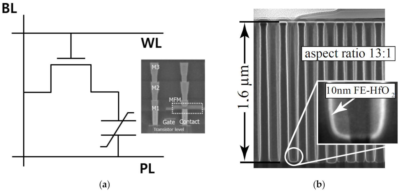
4.2. Ferroelectric Randon Access Memory (FeRAM)

FeRAM is a memory device that stores information based on the characteristics of ferroelectricity and is considered one of the next generation non-volatile memories. Because spontaneous polarization can be induced by an external electric field, ferroelectric materials can have two stable polarization states (positive + Pr, negative – Pr), which can be expressed as logical binaries 0 and 1.
The idea for these ferroelectric memories was first proposed by MIT researchers in 1950 [95]. Since then, FeRAMs have been developed based on perovskite-based materials such as PZT, BTO, and SBT. However, perovskite ferroelectrics have a problem of disappearing polarization as thickness decreases, limiting their use in highly-integrated memory. For PZT, a thickness of at least 100 nm is required to obtain sufficient ferroelectricity, and PZT is not suitable for CMOS processes due to instability and contamination.
The discovery of ferroelectricity in HfO2 suitable for CMOS has revived interest in FeRAM. FeRAM based on ferroelectric HfO2 has a 1T-1C memory cell structure similar to DRAM (Figure 11a). FeRAM can be characterized by measuring switching current depending on polarization, which can be distinguished in a small area of 1/10 compared to DRAM. This reduces the energy required to detect memory states to 1/10, to implement low-power NVMs.
Furthermore, for high integration, 3D integration is required, and HfO2 can make a 3D structure capacitor with a high aspect ratio using the mature ALD technique (Figure 11b) [21,25]. Since FeRAM loses information in the read cycle, it is necessary to rewrite. Because of this destructive memory read-out process, the endurance of the ferroelectric layer (more than 1015) is very important. An optimized perovskite-based FeRAM is known to have an endurance of more than 1016 cycles [96], but unlike PZT, HfO2 has much lower durability (<1010) due to its high coercive field. The high coercive field of ferroelectric HfO2 needed to drive the FeRAM causes high stress, leading to breakdown. Recently studies using la-doped HZO have shown endurance up to 1011 cycles, but they still have low endurance compared to perovskite-based FeRAM [97,98]. In order to manufacture a highly durable HfO2-based FeRAM, it will be necessary to understand structural changes, defects, and internal physical mechanisms in the process.
Figure 11. (a) Schematic of a 1T-1F FeRAM and cross section SEM image of an MFM capacitor integrated by BEOL process. Reproduced with permission [3]. Copyright 2020, IEEE. (b) ferroelectric HfO2 based high aspect ratio 3D 1T-1C FeRAM. Reproduced with permission [99]. Copyright 2013, IEEE.
Electronics 10 02759 g011

4.3. Ferroelectric Tunnel Junction (FTJ)

FTJ is a memory device that uses a few nanometer thick ferroelectric film as a tunneling barrier and changes its resistance depending on its polarization. Unlike FeRAM, which requires rewriting when reading information, FTJ can read information non-destructively, and is also capable of reading and erasing information using very little energy and a few nanoseconds [100]. Esaki et al. first proposed an FTJ under the name ‘polar switch’ in 1970 [101]. However, a very thin film with ferroelectricity was not found, and an actual FTJ was not developed until the 2000s [102]. A successful FTJ using BaTiO3 was demonstrated in 2009 [103].
The ferroelectric layer operates as a memory by switching polarization by increasing (ON state) or lowering (Off state) the conductivity of the junction. The tunneling electroresistance (TER) effect is observed in the ferroelectric thin film as the height of the tunnel barrier changes according to the change in polarization. The TER effect occurs mainly through three mechanisms: Direct tunneling, FN tunneling, and thermal current. In Direct tunneling, electrons pass directly through a tunneling barrier. In FN tunneling, electrons pass between tunneling barriers due to an applied voltage and is a phenomenon that occurs in a relatively thick ferroelectric layer. Thermionic current occurs in a ferroelectric layer thick enough to sufficiently reduce direct tunneling:
T E R = exp 2 m Δ φ φ ¯ d
The TER value is expressed in the following Equation (6), and it has a larger value in a thicker barrier. Therefore, in polarization switching, the FN tunneling mechanism results in a larger TER value than direct tunneling. However, it should be noted that the thick ferroelectric layer affects current density and stable and fast memory operation.
Ferroelectric HfO2 is more suitable for FTJ because it can easily form a thinner ferroelectric layer compared to perovskite. An HfO2-based FTJ made in this way can be applied to neuromorphic devices or memristors as NVM devices [104,105]. However, FTJ based on ferroelectric HfO2 have a small voltage margin when polarization is reversed due to the high Ec value (~1 MV/cm) which causes breakdown and lowers cycling endurance. In addition, high tunneling current that traps electrons can occur during operation. This electron trapping affects the barrier caused by remanent polarization, and lowers the LRS/HRS value. To solve this problem, an improved approach combining dielectric layers has been reported [106].

4.4. Ferroelectric Field-Effect Transistor (FeFET)

The idea to change the conductivity of semiconductor layers using ferroelectrics was proposed in 1957 [107]. In 1960, experimental results with FeFETs were reported, changing the threshold voltage of the FETs using a ferroelectric insulating film [108]. Since then, FeFETs have been extensively studied, with the development of perovskite materials and film growth, but perovskite FETs were not commercialized, even though they were proposed earlier than floating gate memory transistors, due to their many disadvantages when applied to silicon technology [109]. After the discovery of ferroelectric HfO2, the potential for CMOS-based FeFETs has stimulated renewed interest, given ferroelectric HfO2 compatibility with CMOS [6,20,21,22]. Furthermore, recently, ferroelectric HfO2 FeFETs have been demonstrated on 22 nm FDSOI technology using existing HKMG technology and mature ALD [20]. In addition, FeFETs have been applied to various applications, such as NVM, neuromorphic, and logic-in memory computing [110,111,112].
Similar to flash memory, the conductivity of the channel is changed by the polarization of the ferroelectric layer, to induce a low threshold voltage (LVT) or a high threshold voltage (HVT). Since the memory window is determined to be 2 × Ec × t (t is thickness), a high Ec value is required. HfO2 generally has an Ec value of 1 MV/cm, and assuming that the thickness is 5 nm, the achievable memory window is about 1 V. The high Ec value of HfO2 has great advantages for scaling and memory windows, but it brings disadvantages for retention and endurance.
The pulse voltage of the program/erase (PGM/ERS) process causes a strong electric field to be applied to the very thin HfO2 thin film, which reduces endurance. In addition, it is known that trapped charges appearing at the interface during the PGM and ERS processes reduce data retention [113,114]. However, even if the reduction of endurance at the interface is solved, this does not solve the fundamentally low endurance of 107, so new structure and methods must be introduced, such as the introduction of MFMIS structure or subloop driving. Obtaining a sufficient number of ferroelectric domains at very small scale will likely require the introduction of 3D structures.

5. Conclusions

The unexpected discovery of ferroelectricity in HfO2 has revived interest in non-volatile memory. Ferroelectric HfO2 can be fabricated by inducing an orthorhombic phase using various dopants and deposition methods. In order to obtain a uniform film on the entire surface, it seems that among various materials Zr is suitable for Hf doping because its atomic structure and atomic radius are similar. Since heat treatment is required in the crystallization process after deposition, there are limitations on the structure and application range of the device. If ferroelectricity can be derived through a low temperature process with various heat sources and pretreatment processes, it would be possible to apply ferroelectric HfO2 to various electronic devices such as flexible devices as well as to the BEOL process. Ferroelectric HfO2 can be analyzed using various measurements such as P–V loop, PFM XRD, and TEM, which can be the basis for improving endurance and performance as well as understanding physical characteristics.
Ferroelectric gated FETs with the NC effect enable low power CMOS logic devices. Ferroelectric HfO2 thin film is CMOS compatible and has been applied in sub-5 nm technology, so supply voltage can be lower than 0.5 V. The ‘Boltzmann tyranny’ can be overcome by driving the device below 60 mV/dec with a steep subthreshold swing. FeRAM has a very fast access time, and 10 ns can be realized. FTJ can be used as a multi-level brain-like device, as well as to improve understanding of the polarization switching mechanism. FeFETs can also be applied to non-volatile memory devices, if the characteristics and endurance of the film are sufficiently improved. An FeFET with a 1 T structure enables high-density integration, implementing the same functions as an existing 14 T CPU register and 6 T SRAM. Ferroelectrics do not allow a device with a simple memory function, but a multi-functional device can be used in various ways, such as NCFET, neurocomputing, in-memory computing, and analog computing. By applying FeFETs to high-performance, low-energy, high-density, and integrated logic devices, they are expected to be used as a next generation NVM device for AI computing and data processor.

Author Contributions

Conceptualization, C.-M.S. and H.-J.K.; investigation, C.-M.S. and H.-J.K.; writing-original draft preparation, C.-M.S.; writing-review and editing, C.-M.S. and H.-J.K. All authors contributed to the present paper with the same effort in finding available literature resources, as well as writing the paper. All authors have read and agreed to the published version of the manuscript.

Funding

This work was supported by the Next-Generation Intelligent Semiconductor Technology Development Program through the National Research Foundation of Korea (NRF) funded by Ministry of Science and ICT (2020M3F3A2A02082437) and by the Basic Science Research Program through NRF funded by the MSIT (2019M3C1B8090840 and 2019R1F1A1061883). This work was also performed under the DGIST R&D Program of the Ministry of Science and ICT (21-IJRP-01).

Data Availability Statement

Not applicable.

Conflicts of Interest

The authors declare no conflict of interest.

References

  1. Keshavarzi, A.; Ni, K.; Van Den Hoek, W.; Datta, S.; Raychowdhury, A. Ferroelectronics for edge intelligence. IEEE Micro 2020, 40, 33–48. [Google Scholar] [CrossRef]
  2. Lines, M.E.; Glass, A.M. Principles and Applications of Ferroelectrics and Related Materials; Oxford University Press: New York, NY, USA, 2001. [Google Scholar]
  3. Okuno, J.; Kunihiro, T.; Konishi, K.; Maemura, H.; Shute, Y.; Sugaya, F.; Materano, M.; Ali, T.; Kuehnel, K.; Seide, K. SoC compatible 1T1C FeRAM memory array based on ferroelectric Hf0.5Zr0.5O2. In Proceedings of the 2020 IEEE Symposium on VLSI Technology, Honolulu, HI, USA, 16–19 June 2020; pp. 1–2. [Google Scholar]
  4. Okuno, J.; Kunihiro, T.; Konishi, K.; Maemura, H.; Shuto, Y.; Sugaya, F.; Materano, M.; Ali, T.; Lederer, M.; Kuehnel, K. High-Endurance and Low-Voltage operation of 1T1C FeRAM Arrays for Nonvolatile Memory Application. In Proceedings of the 2021 IEEE International Memory Workshop, Dresden, Germany, 16–19 May 2021; pp. 1–3. [Google Scholar]
  5. Jerry, M.; Chen, P.-Y.; Zhang, J.; Sharma, P.; Ni, K.; Yu, S.; Datta, S. Ferroelectric FET analog synapse for acceleration of deep neural network training. In Proceedings of the 2017 IEEE International Electron Devices Meeting, San Francisco, CA, USA, 2–6 December 2017; pp. 6.2.1–6.2.4. [Google Scholar]
  6. Sun, X.; Wang, P.; Ni, K.; Datta, S.; Yu, S. Exploiting hybrid precision for training and inference: A 2T-1FeFET based analog synaptic weight cell. In Proceedings of the 2018 IEEE International Electron Devices Meeting, San Francisco, CA, USA, 1–5 December 2018; pp. 3.1.1–3.1.4. [Google Scholar]
  7. Fong, D.D.; Stephenson, G.B.; Streiffer, S.K.; Eastman, J.A.; Auciello, O.; Fuoss, P.H.; Thompson, C. Ferroelectricity in ultrathin perovskite films. Science 2004, 304, 1650–1653. [Google Scholar] [CrossRef]
  8. Scott, J. Applications of modern ferroelectrics. Science 2007, 315, 954–959. [Google Scholar] [CrossRef] [PubMed]
  9. Ihlefeld, J.F.; Harris, D.T.; Keech, R.; Jones, J.L.; Maria, J.P.; Trolier-McKinstry, S. Scaling effects in perovskite ferroelectrics: Fundamental limits and process-structure-property relations. J. Am. Ceram. Soc. 2016, 99, 2537–2557. [Google Scholar] [CrossRef]
  10. Böscke, T.; Müller, J.; Bräuhaus, D.; Schröder, U.; Böttger, U. Ferroelectricity in hafnium oxide thin films. Appl. Phys. Lett. 2011, 99, 102903. [Google Scholar] [CrossRef]
  11. Cheynet, M.C.; Pokrant, S.; Tichelaar, F.D.; Rouvière, J.-L. Crystal structure and band gap determination of HfO2 thin films. J. Appl. Phys. 2007, 101, 054101. [Google Scholar] [CrossRef] [Green Version]
  12. Khanna, S.; Bartling, S.C.; Clinton, M.; Summerfelt, S.; Rodriguez, J.A.; McAdams, H.P. An FRAM-Based Nonvolatile Logic MCU SoC Exhibiting 100% Digital State Retention at VDD = 0 V Achieving Zero Leakage with <400-ns Wakeup Time for ULP Applications. IEEE J. Solid State Circuits 2013, 49, 95–106. [Google Scholar]
  13. Koo, J.-M.; Seo, B.-S.; Kim, S.; Shin, S.; Lee, J.-H.; Baik, H.; Lee, J.-H.; Lee, J.H.; Bae, B.-J.; Lim, J.-E. Fabrication of 3D trench PZT capacitors for 256Mbit FRAM device application. In Proceedings of the IEEE InternationalElectron Devices Meeting, 2005. IEDM Technical Digest, Washington, DC, USA, 5 December 2005; pp. 4–343. [Google Scholar]
  14. McAdams, H.P.; Acklin, R.; Blake, T.; Du, X.-H.; Eliason, J.; Fong, J.; Kraus, W.F.; Liu, D.; Madan, S.; Moise, T. A 64-Mb embedded FRAM utilizing a 130-nm 5LM Cu/FSG logic process. IEEE J. Solid State Circuits 2004, 39, 667–677. [Google Scholar] [CrossRef]
  15. Boyn, S.; Grollier, J.; Lecerf, G.; Xu, B.; Locatelli, N.; Fusil, S.; Girod, S.; Carrétéro, C.; Garcia, K.; Xavier, S. Learning through ferroelectric domain dynamics in solid-state synapses. Nat. Commun. 2017, 8, 14736. [Google Scholar] [CrossRef]
  16. Cervo Sulzbach, M.; Tan, H.; Estandía, S.; Gàzquez, J.; Sánchez, F.; Fina, I.; Fontcuberta, J. Polarization and Resistive Switching in Epitaxial 2nm Hf 0.5Zr0.5O2 Tunnel Junctions. ACS Appl. Electron. Mater. 2021, 3, 3657–3666. [Google Scholar] [CrossRef]
  17. Gajek, M.; Bibes, M.; Fusil, S.; Bouzehouane, K.; Fontcuberta, J.; Barthelemy, A.; Fert, A. Tunnel junctions with multiferroic barriers. Nat. Mater. 2007, 6, 296–302. [Google Scholar] [CrossRef] [PubMed]
  18. Li, J.; Li, N.; Ge, C.; Huang, H.; Sun, Y.; Gao, P.; He, M.; Wang, C.; Yang, G.; Jin, K. Giant electroresistance in ferroionic tunnel junctions. IScience 2019, 16, 368–377. [Google Scholar] [CrossRef] [Green Version]
  19. Yoon, C.; Lee, J.H.; Lee, S.; Jeon, J.H.; Jang, J.T.; Kim, D.H.; Kim, Y.H.; Park, B.H. Synaptic plasticity selectively activated by polarization-dependent energy-efficient ion migration in an ultrathin ferroelectric tunnel junction. Nano Lett. 2017, 17, 1949–1955. [Google Scholar] [CrossRef]
  20. Dünkel, S.; Trentzsch, M.; Richter, R.; Moll, P.; Fuchs, C.; Gehring, O.; Majer, M.; Wittek, S.; Müller, B.; Melde, T. A FeFET based super-low-power ultra-fast embedded NVM technology for 22 nm FDSOI and beyond. In Proceedings of the 2017 IEEE International Electron Devices Meeting, San Francisco, CA, USA, 2–6 December 2017; pp. 19.7.1–19.7.4. [Google Scholar]
  21. Florent, K.; Pesic, M.; Subirats, A.; Banerjee, K.; Lavizzari, S.; Arreghini, A.; Di Piazza, L.; Potoms, G.; Sebaai, F.; McMitchell, S. Vertical ferroelectric HfO2 FET based on 3-D NAND architecture: Towards dense low-power memory. In Proceedings of the 2018 IEEE International Electron Devices Meeting, San Francisco, CA, USA, 1–5 December 2018; pp. 2.5.1–2.5.4. [Google Scholar]
  22. Mulaosmanovic, H.; Breyer, E.T.; Mikolajick, T.; Slesazeck, S. Reconfigurable frequency multiplication with a ferroelectric transistor. Nat. Electron. 2020, 3, 391–397. [Google Scholar] [CrossRef]
  23. Schroeder, U.; Hwang, C.S.; Funakubo, H. Ferroelectricity in Doped Hafnium Oxide: Materials, Properties and Devices; Woodhead Publishing: Cambridge, UK, 2019. [Google Scholar]
  24. George, S.M. Atomic layer deposition: An overview. Chem. Rev. 2010, 110, 111–131. [Google Scholar] [CrossRef] [PubMed]
  25. Polakowski, P.; Riedel, S.; Weinreich, W.; Rudolf, M.; Sundqvist, J.; Seidel, K.; Muller, J. Ferroelectric deep trench capacitors based on Al: HfO2 for 3D nonvolatile memory applications. In Proceedings of the 2014 IEEE 6th International Memory Workshop, Taipei, Taiwan, 18–21 May 2014; pp. 1–4. [Google Scholar]
  26. Schroeder, U.; Yurchuk, E.; Müller, J.; Martin, D.; Schenk, T.; Polakowski, P.; Adelmann, C.; Popovici, M.I.; Kalinin, S.V.; Mikolajick, T. Impact of different dopants on the switching properties of ferroelectric hafniumoxide. Jpn. J. Appl. Phys. 2014, 53, 08LE02. [Google Scholar] [CrossRef]
  27. Clima, S.; Wouters, D.; Adelmann, C.; Schenk, T.; Schroeder, U.; Jurczak, M.; Pourtois, G. Identification of the ferroelectric switching process and dopant-dependent switching properties in orthorhombic HfO2: A first principles insight. Appl. Phys. Lett. 2014, 104, 092906. [Google Scholar] [CrossRef]
  28. Lederer, M.; Kämpfe, T.; Olivo, R.; Lehninger, D.; Mart, C.; Kirbach, S.; Ali, T.; Polakowski, P.; Roy, L.; Seidel, K. Local crystallographic phase detection and texture mapping in ferroelectric Zr doped HfO2 films by transmission-EBSD. Appl. Phys. Lett. 2019, 115, 222902. [Google Scholar] [CrossRef]
  29. Pešić, M.; Fengler, F.P.G.; Larcher, L.; Padovani, A.; Schenk, T.; Grimley, E.D.; Sang, X.; LeBeau, J.M.; Slesazeck, S.; Schroeder, U. Physical mechanisms behind the field-cycling behavior of HfO2-based ferroelectric capacitors. Adv. Funct. Mater. 2016, 26, 4601–4612. [Google Scholar] [CrossRef]
  30. Ni, K.; Chakraborty, W.; Smith, J.; Grisafe, B.; Datta, S. Fundamental understanding and control of device-to-device variation in deeply scaled ferroelectric FETs. In Proceedings of the 2019 Symposium on VLSI Technology, Kyoto, Japan, 9–14 June 2019; pp. T40–T41. [Google Scholar]
  31. Hoffmann, M.; Schroeder, U.; Schenk, T.; Shimizu, T.; Funakubo, H.; Sakata, O.; Pohl, D.; Drescher, M.; Adelmann, C.; Materlik, R. Stabilizing the ferroelectric phase in doped hafnium oxide. J. Appl. Phys. 2015, 118, 072006. [Google Scholar] [CrossRef]
  32. Wasa, K.; Hayakawa, S. Handbook of Sputter Deposition Technology; Noyes Publications: New York, NY, USA, 1992. [Google Scholar]
  33. Olsen, T.; Schröder, U.; Müller, S.; Krause, A.; Martin, D.; Singh, A.; Müller, J.; Geidel, M.; Mikolajick, T. Co-sputtering yttrium into hafnium oxide thin films to produce ferroelectric properties. Appl. Phys. Lett. 2012, 101, 082905. [Google Scholar] [CrossRef]
  34. Xu, L.; Nishimura, T.; Shibayama, S.; Yajima, T.; Migita, S.; Toriumi, A. Kinetic pathway of the ferroelectric phase formation in doped HfO2 films. J. Appl. Phys. 2017, 122, 124104. [Google Scholar] [CrossRef]
  35. Mittmann, T.; Materano, M.; Lomenzo, P.D.; Park, M.H.; Stolichnov, I.; Cavalieri, M.; Zhou, C.; Chung, C.C.; Jones, J.L.; Szyjka, T. Origin of ferroelectric phase in undoped HfO2 films deposited by sputtering. Adv. Mater. Interfaces 2019, 6, 1900042. [Google Scholar] [CrossRef] [Green Version]
  36. Kim, K.; Park, M.; Kim, H.; Kim, Y.; Moon, T.; Lee, Y.; Hyun, S.; Gwon, T.; Hwang, C. Ferroelectricity in undoped-HfO2 thin films induced by deposition temperature control during atomic layer deposition. J. Mater. Chem. C 2016, 4, 6864–6872. [Google Scholar] [CrossRef]
  37. Park, M.H.; Lee, D.H.; Yang, K.; Park, J.-Y.; Yu, G.T.; Park, H.W.; Materano, M.; Mittmann, T.; Lomenzo, P.D.; Mikolajick, T. Review of defect chemistry in fluorite-structure ferroelectrics for future electronic devices. J. Mater. Chem. C 2020, 8, 10526–10550. [Google Scholar] [CrossRef]
  38. Liang, H.; Zhang, B.; Guo, Y.; Guo, X.; Ren, S.; Li, Y.; Lu, Y.; Lang, R. New approach for fabrication of annealing-free ferroelectric HfO2-based films at room temperature. Ceram. Int. 2021, 47, 27843–27848. [Google Scholar] [CrossRef]
  39. Mimura, T.; Shimizu, T.; Uchida, H.; Funakubo, H. Room-temperature deposition of ferroelectric HfO2-based films by the sputtering method. Appl. Phys. Lett. 2020, 116, 062901. [Google Scholar] [CrossRef]
  40. Eason, R. Pulsed Laser Deposition of Thin Films: Applications-Led Growth of Functional Materials; John Wiley & Sons: Hoboken, NJ, USA, 2007. [Google Scholar]
  41. Lyu, J.; Song, T.; Fina, I.; Sánchez, F. High polarization, endurance and retention in sub-5 nm Hf0.5Zr0.5O2 films. Nanoscale 2020, 12, 11280–11287. [Google Scholar] [CrossRef]
  42. Shimizu, T.; Katayama, K.; Kiguchi, T.; Akama, A.; Konno, T.J.; Funakubo, H. Growth of epitaxial orthorhombic YO1.5-substituted HfO2 thin film. Appl. Phys. Lett. 2015, 107, 032910. [Google Scholar] [CrossRef]
  43. Wang, B.; Leonardi, M.J.; Huang, W.; Chen, Y.; Zeng, L.; Eckstein, B.J.; Marks, T.J.; Facchetti, A. Marked cofuel tuning of combustion synthesis pathways for metal oxide semiconductor films. Adv. Electron. Mater. 2019, 5, 1900540. [Google Scholar] [CrossRef]
  44. Yoong, H.Y.; Wu, H.; Zhao, J.; Wang, H.; Guo, R.; Xiao, J.; Zhang, B.; Yang, P.; Pennycook, S.J.; Deng, N. Epitaxial Ferroelectric Hf0.5Zr0.5O2 Thin Films and Their Implementations in Memristors for Brain-Inspired Computing. Adv. Funct. Mater. 2018, 28, 1806037. [Google Scholar] [CrossRef]
  45. Hench, L.L.; West, J.K. The sol-gel process. Chem. Rev. 1990, 90, 33–72. [Google Scholar] [CrossRef]
  46. Vest, R.W. Metallo-organic decomposition (MOD) processing of ferroelectric and electro-optic films: A review. Ferroelectrics 1990, 102, 53–68. [Google Scholar] [CrossRef]
  47. Abe, C.; Nakayama, S.; Shiokawa, M.; Kawashima, H.; Katayama, K.; Shiraishi, T.; Shimizu, T.; Funakubo, H.; Uchida, H. Crystal structure and dielectric/ferroelectric properties of CSD-derived HfO2-ZrO2 solid solution films. Ceram. Int. 2017, 43, S501–S505. [Google Scholar] [CrossRef]
  48. Chen, H.; Chen, Y.; Tang, L.; Luo, H.; Zhou, K.; Yuan, X.; Zhang, D. Obvious ferroelectricity in undoped HfO2 films by chemical solution deposition. J. Mater. Chem. C 2020, 8, 2820–2826. [Google Scholar] [CrossRef]
  49. Hasan, M.M.; Ahn, C.W.; Kim, T.H.; Jang, J. Solution processed high performance ferroelectric Hf0.5Zr0.5O2 thin film transistor on glass substrate. Appl. Phys. Lett. 2021, 118, 152901. [Google Scholar] [CrossRef]
  50. Kim, S.; Hong, J. Ferroelectricity in ultrathin yttrium-doped hafnium oxide films prepared by chemical solution deposition based on metal chlorides and alcohol. Ceram. Int. 2017, 43, S158–S161. [Google Scholar] [CrossRef]
  51. Miyasako, T.; Tokumitsu, E. Indium oxide and indium-tin-oxide channel ferroelectric gate thin film transistors with yttrium doped hafnium-zirconium dioxide gate insulator prepared by chemical solution process. Jpn. J. Appl. Phys. 2021, 60, SBBM02. [Google Scholar]
  52. Murakami, T.; Haga, K.-i.; Tokumitsu, E. Impact of annealing environment on electrical properties of yttrium-doped hafnium zirconium dioxide thin films prepared by the solution process. Jpn. J. Appl. Phys. 2020, 59, SPPB03. [Google Scholar]
  53. Nakayama, S.; Funakubo, H.; Uchida, H. Crystallization behavior and ferroelectric property of HfO2–ZrO2 films fabricated by chemical solution deposition. Jpn. J. Appl. Phys. 2018, 57, 11UF06. [Google Scholar] [CrossRef]
  54. Pujar, P.; Cho, H.; Gandla, S.; Naqi, M.; Hong, S.; Kim, S. Sub-Thermionic Negative Capacitance Field Effect Transistors with Solution Combustion-Derived Hf0.5Zr0.5O2. Adv. Funct. Mater. 2021, 31, 2103748. [Google Scholar] [CrossRef]
  55. Starschich, S.; Boettger, U. An extensive study of the influence of dopants on the ferroelectric properties of HfO2. J. Mater. Chem. C 2017, 5, 333–338. [Google Scholar] [CrossRef]
  56. Starschich, S.; Griesche, D.; Schneller, T.; Böttger, U. Chemical solution deposition of ferroelectric hafnium oxide for future lead free ferroelectric devices. ECS J. Solid State Sci. Technol. 2015, 4, P419–P423. [Google Scholar] [CrossRef]
  57. Starschich, S.; Griesche, D.; Schneller, T.; Waser, R.; Böttger, U. Chemical solution deposition of ferroelectric yttrium-doped hafnium oxide films on platinum electrodes. Appl. Phys. Lett. 2014, 104, 202903. [Google Scholar] [CrossRef] [Green Version]
  58. Wang, J.; Zhou, D.; Dong, W.; Yao, Y.; Sun, N.; Ali, F.; Hou, X.; Liu, F. Optimizing Annealing Process for Ferroelectric Y-Doped HfO2 Thin Films by All-Inorganic Aqueous Precursor Solution. Adv. Electron. Mater. 2021, 7, 2000585. [Google Scholar] [CrossRef]
  59. Wei, A.; Chen, C.; Tang, L.; Zhou, K.; Zhang, D. Chemical solution deposition of ferroelectric Sr: HfO2 film from inorganic salt precursors. J. Alloy. Compd. 2018, 731, 546–553. [Google Scholar] [CrossRef]
  60. Bretos, I.; Jiménez, R.; Ricote, J.; Calzada, M.L. Low-temperature crystallization of solution-derived metal oxide thin films assisted by chemical processes. Chem. Soc. Rev. 2018, 47, 291–308. [Google Scholar] [CrossRef] [Green Version]
  61. Das, D.; Buyantogtokh, B.; Gaddam, V.; Jeon, S. Influence of High-Pressure Annealing Conditions on Ferroelectric and Interfacial Properties of Zr-Rich HfₓZr₁₋ ₓO₂Capacitors. IEEE Trans. Electron Devices 2021, 68, 1996–2002. [Google Scholar] [CrossRef]
  62. Lee, Y.H.; Hyun, S.D.; Kim, H.J.; Kim, J.S.; Yoo, C.; Moon, T.; Kim, K.D.; Park, H.W.; Lee, Y.B.; Kim, B.S. Nucleation-Limited Ferroelectric Orthorhombic Phase Formation in Hf0.5Zr0.5O2 Thin Films. Adv. Electron. Mater. 2019, 5, 1800436. [Google Scholar] [CrossRef]
  63. Lehninger, D.; Olivo, R.; Ali, T.; Lederer, M.; Kämpfe, T.; Mart, C.; Biedermann, K.; Kühnel, K.; Roy, L.; Kalkani, M. Back-End-of-Line Compatible Low-Temperature Furnace Anneal for Ferroelectric Hafnium Zirconium Oxide Formation. Phys. Status Solidi (A) 2020, 217, 1900840. [Google Scholar] [CrossRef] [Green Version]
  64. Yu, H.; Chung, C.C.; Shewmon, N.; Ho, S.; Carpenter, J.H.; Larrabee, R.; Sun, T.; Jones, J.L.; Ade, H.; O’Connor, B.T. Flexible inorganic ferroelectric thin films for nonvolatile memory devices. Adv. Funct. Mater. 2017, 27, 1700461. [Google Scholar] [CrossRef]
  65. O’Connor, É.; Halter, M.; Eltes, F.; Sousa, M.; Kellock, A.; Abel, S.; Fompeyrine, J. Stabilization of ferroelectric HfxZr1-xO2 films using a millisecond flash lamp annealing technique. APL Mater. 2018, 6, 121103. [Google Scholar] [CrossRef] [Green Version]
  66. Grenouillet, L.; Francois, T.; Coignus, J.; Kerdilès, S.; Vaxelaire, N.; Carabasse, C.; Mehmood, F.; Chevalliez, S.; Pellissier, C.; Triozon, F. Nanosecond Laser Anneal (NLA) for Si-implanted HfO2 Ferroelectric Memories Integrated in Back-End of Line (BEOL). In Proceedings of the 2020 IEEE Symposium on VLSI Technology, Honolulu, HI, USA, 16–19 June 2020; pp. 1–2. [Google Scholar]
  67. Volodina, N.; Dmitriyeva, A.; Chouprik, A.; Gatskevich, E.; Zenkevich, A. Ferroelectric Hf0.5Zr0.5O2 Thin Films Crystallized by Pulsed Laser Annealing. Phys. Status Solidi Rapid Res. Lett. 2021, 15, 2100082. [Google Scholar] [CrossRef]
  68. Hsain, H.A.; Sharma, P.; Yu, H.; Jones, J.L.; So, F.; Seidel, J. Enhanced piezoelectricity of thin film hafnia-zirconia (HZO) by inorganic flexible substrates. Appl. Phys. Lett. 2018, 113, 022905. [Google Scholar] [CrossRef]
  69. Liu, H.; Lu, T.; Li, Y.; Ju, Z.; Zhao, R.; Li, J.; Shao, M.; Zhang, H.; Liang, R.; Wang, X.R. Flexible Quasi-van der Waals Ferroelectric Hafnium-Based Oxide for Integrated High-Performance Nonvolatile Memory. Adv. Sci. 2020, 7, 2001266. [Google Scholar] [CrossRef]
  70. Joh, H.; Anoop, G.; Lee, W.-J.; Das, D.; Lee, J.Y.; Kim, T.Y.; Kim, H.; Seol, W.; Yeom, J.; Jeon, S. Low-Temperature Growth of Ferroelectric Hf0.5Zr0.5O2 Thin Films Assisted by Deep Ultraviolet Light Irradiation. ACS Appl. Electron. Mater. 2021, 3, 1244–1251. [Google Scholar] [CrossRef]
  71. Gaddam, V.; Das, D.; Jung, T.; Jeon, S. Ferroelectricity Enhancement in Hf0.5Zr0.5O2 Based Tri-Layer Capacitors at Low-Temperature (350 °C) Annealing Process. IEEE Electron Device Lett. 2021, 42, 812–815. [Google Scholar] [CrossRef]
  72. Hur, J.; Luo, Y.-C.; Tasneem, N.; Khan, A.I.; Yu, S. Ferroelectric Hafnium Zirconium Oxide Compatible With Back-End-of-Line Process. IEEE Trans. Electron Devices 2021, 68, 3176–3180. [Google Scholar] [CrossRef]
  73. Kim, S.; Narayan, D.; Lee, J.-G.; Mohan, J.; Lee, J.S.; Lee, J.; Young, C.; Kim, J.; Summerfelt, S.; San, T.; et al. Low Temperature (400 °C) Ferroelectric Hf0.5Zr0.5O2 Capacitors for Next-Generation FRAM Applications. In Proceedings of the 2017 IEEE International Memory Workshop, Monterey, CA, USA, 14–17 May 2017; pp. 1–4. [Google Scholar]
  74. Muller, J.; Boscke, T.S.; Schroder, U.; Mueller, S.; Brauhaus, D.; Bottger, U.; Frey, L.; Mikolajick, T. Ferroelectricity in simple binary ZrO2 and HfO2. Nano Lett. 2012, 12, 4318–4323. [Google Scholar] [CrossRef]
  75. Zhou, D.; Guan, Y.; Vopson, M.; Xu, J.; Liang, H.; Cao, F.; Dong, X.; Mueller, J.; Schenk, T.; Schroeder, U. Electric field and temperature scaling of polarization reversal in silicon doped hafnium oxide ferroelectric thin films. Acta Mater. 2015, 99, 240–246. [Google Scholar] [CrossRef] [Green Version]
  76. Guethner, P.; Dransfeld, K. Local poling of ferroelectric polymers by scanning force microscopy. Appl. Phys. Lett. 1992, 61, 1137–1139. [Google Scholar] [CrossRef]
  77. Cheema, S.S.; Kwon, D.; Shanker, N.; Dos Reis, R.; Hsu, S.-L.; Xiao, J.; Zhang, H.; Wagner, R.; Datar, A.; McCarter, M.R. Enhanced ferroelectricity in ultrathin films grown directly on silicon. Nature 2020, 580, 478–482. [Google Scholar] [CrossRef]
  78. Park, M.H.; Chung, C.-C.; Schenk, T.; Richter, C.; Opsomer, K.; Detavernier, C.; Adelmann, C.; Jones, J.L.; Mikolajick, T.; Schroeder, U. Effect of Annealing Ferroelectric HfO2 Thin Films: In Situ, High Temperature X-Ray Diffraction. Adv. Electron. Mater. 2018, 4, 1800091. [Google Scholar] [CrossRef]
  79. Fields, S.S.; Smith, S.W.; Ryan, P.J.; Jaszewski, S.T.; Brummel, I.A.; Salanova, A.; Esteves, G.; Wolfley, S.L.; Henry, M.D.; Davids, P.S. Phase-Exchange-Driven Wake-Up and Fatigue in Ferroelectric Hafnium Zirconium Oxide Films. ACS Appl. Mater. Interfaces 2020, 12, 26577–26585. [Google Scholar] [CrossRef]
  80. Grimley, E.; Schenk, T.; Sang, X.; Pfaj, M.; Schroeder, U.; Mikolajick, T.; Lebeau, J. Structural Changes Underlying Field Cycling Phenomena in Ferroelectric HfO2 Thin Films. Adv. Electron. Mater. 2016, 2, 1600173. [Google Scholar] [CrossRef]
  81. Sang, X.; Grimley, E.; Schenk, T.; Schroeder, U.; Lebeau, J. On the structural origins of ferroelectricity in HfO2 thin films. Appl. Phys. Lett. 2015, 106, 162905. [Google Scholar] [CrossRef]
  82. Khan, A.I.; Keshavarzi, A.; Datta, S. The future of ferroelectric field-effect transistor technology. Nat. Electron. 2020, 3, 588–597. [Google Scholar] [CrossRef]
  83. Devonshire, A.F. XCVI. Theory of barium titanate. Philos. Mag. Ser. 1949, 40, 1040–1063. [Google Scholar] [CrossRef]
  84. Landau, L.D.; Khalatnikov, I.M. On the anomalous absorption of sound near a second order phase transition point. Dokl. Akad. Nauk. SSSR 1954, 96, 469–472. [Google Scholar]
  85. Salahuddin, S.; Datta, S. Use of negative capacitance to provide voltage amplification for low power nanoscale devices. Nano Lett. 2008, 82, 405–410. [Google Scholar] [CrossRef] [PubMed]
  86. Saeidi, A.; Jazaeri, F.; Stolichnov, I.; Enz, C.C.; Ionescu, A.M. Negative capacitance as universal digital and analog performance booster for complementary MOS transistors. Sci. Rep. 2019, 9, 9105. [Google Scholar] [CrossRef] [Green Version]
  87. Chatterjee, K.; Rosner, A.J.; Salahuddin, S. Intrinsic speed limit of negative capacitance transistors. IEEE Electron Device Lett. 2017, 38, 1328–1330. [Google Scholar] [CrossRef]
  88. Cheng, C.-H.; Chin, A. Low-Voltage Steep Turn-On pMOSFET Using Ferroelectric High- κ Gate Dielectric. IEEE Electron Device Lett. 2014, 35, 274–276. [Google Scholar] [CrossRef]
  89. Kwon, D.; Chatterjee, K.; Tan, A.J.; Yadav, A.K.; Zhou, H.; Sachid, A.B.; Dos Reis, R.; Hu, C.; Salahuddin, S. Improved subthreshold swing and short channel effect in FDSOI n-channel negative capacitance field effect transistors. IEEE Electron Device Lett. 2017, 39, 300–303. [Google Scholar] [CrossRef]
  90. McGuire, F.A.; Lin, Y.-C.; Price, K.; Rayner, G.B.; Khandelwal, S.; Salahuddin, S.; Franklin, A.D. Sustained sub-60 mV/decade switching via the negative capacitance effect in MoS2 transistors. Nano Lett. 2017, 17, 4801–4806. [Google Scholar] [CrossRef]
  91. Si, M.; Su, C.; Jiang, C.; Conrad, N.; Zhou, H.; Maize, K.; Qiu, G.; Wu, C.; Shakouri, A.; Alam, M.; et al. Steep-slope hysteresis-free negative capacitance MoS2 transistors. Nat. Nanotechnol. 2017, 13, 24–28. [Google Scholar] [CrossRef] [Green Version]
  92. Zhang, Z.; Xu, G.; Zhang, Q.; Hou, Z.; Li, J.; Kong, Z.; Zhang, Y.; Xiang, J.; Xu, Q.; Wu, Z.; et al. FinFET With Improved Subthreshold Swing and Drain Current Using 3-nm Ferroelectric Hf0.5Zr0.5O2. IEEE Electron Device Lett. 2019, 40, 367–370. [Google Scholar] [CrossRef]
  93. Krivokapic, Z.; Rana, U.; Galatage, R.; Razavieh, A.; Aziz, A.; Liu, J.; Shi, J.; Kim, H.; Sporer, R.; Serrao, C. 14nm ferroelectric FinFET technology with steep subthreshold slope for ultra low power applications. In Proceedings of the 2017 IEEE International Electron Devices Meeting, San Francisco, CA, USA, 2–6 December 2017; pp. 15.1.1–15.1.4. [Google Scholar]
  94. Lee, M.; Chen, K.-T.; Liao, C.-Y.; Gu, S.-S.; Siang, G.-Y.; Chou, Y.-C.; Chen, H.-Y.; Le, J.; Hong, R.-C.; Wang, Z.-Y. Extremely steep switch of negative-capacitance nanosheet GAA-FETs and FinFETs. In Proceedings of the 2018 IEEE International Electron Devices Meeting, San Francisco, CA, USA, 1–5 December 2018; pp. 31.8.1–31.8.4. [Google Scholar]
  95. Buck, D.A. Ferroelectrics for Digital Information Storage and Switching; Massachusetts Institute of Technology Cambridge Digital Computer Lab: Cambridge, MA, USA, 1952. [Google Scholar]
  96. Jung, D.; Ahn, W.; Hong, Y.; Kim, H.; Kang, Y.; Kang, J.; Lee, E.; Ko, H.; Kim, S.; Jung, W. An endurance-free ferroelectric random access memory as a non-volatile RAM. In Proceedings of the 2008 Symposium on VLSI Technology, Honolulu, HI, USA, 17–19 June 2008; pp. 102–103. [Google Scholar]
  97. Chernikova, A.G.; Kozodaev, M.G.; Negrov, D.V.; Korostylev, E.V.; Park, M.H.; Schroeder, U.; Hwang, C.S.; Markeev, A.M. Improved ferroelectric switching endurance of La-doped Hf0.5Zr0.5O2 thin films. ACS Appl. Mater. Interfaces 2018, 10, 2701–2708. [Google Scholar] [CrossRef] [PubMed]
  98. Kozodaev, M.G.; Chernikova, A.G.; Korostylev, E.V.; Park, M.H.; Khakimov, R.R.; Hwang, C.S.; Markeev, A.M. Mitigating wakeup effect and improving endurance of ferroelectric HfO2-ZrO2 thin films by careful La-doping. J. Appl. Phys. 2019, 125, 034101. [Google Scholar] [CrossRef]
  99. Muller, J.; Boscke, T.; Muller, S.; Yurchuk, E.; Polakowski, P.; Paul, J.; Martin, D.; Schenk, T.; Khullar, K.; Kersch, A.; et al. Ferroelectric hafnium oxide: A CMOS-compatible and highly scalable approach to future ferroelectric memories. In Proceedings of the 2013 IEEE International Electron Devices Meeting, Washington, DC, USA, 9–11 December 2013; pp. 10.8.1–10.8.4. [Google Scholar]
  100. Chanthbouala, A.; Crassous, A.; Garcia, V.; Bouzehouane, K.; Fusil, S.; Moya, X.; Allibe, J.; Dlubak, B.; Grollier, J.; Xavier, S. Solid-state memories based on ferroelectric tunnel junctions. Nat. Nanotechnol. 2012, 7, 101–104. [Google Scholar] [CrossRef] [PubMed]
  101. Esaki, A.L.; Laibowitz, R.; Stiles, P. Polar switch. IBM Tech. Discl. Bull 1971, 13, 114. [Google Scholar]
  102. Junquera, J.; Ghosez, P. Critical thickness for ferroelectricity in perovskite ultrathin films. Nature 2003, 422, 506–509. [Google Scholar] [CrossRef] [PubMed]
  103. Garcia, V.; Fusil, S.; Bouzehouane, K.; Enouz-Vedrenne, S.; Mathur, N.D.; Barthelemy, A.; Bibes, M. Giant tunnel electroresistance for non-destructive readout of ferroelectric states. Nature 2009, 460, 81–84. [Google Scholar] [CrossRef]
  104. Chen, L.; Wang, T.-Y.; Dai, Y.-W.; Cha, M.-Y.; Zhu, H.; Sun, Q.-Q.; Ding, S.-J.; Zhou, P.; Chua, L.; Zhang, D.W. Ultra-low power Hf0.5Zr0.5O2 based ferroelectric tunnel junction synapses for hardware neural network applications. Nanoscale 2018, 10, 15826–15833. [Google Scholar] [CrossRef]
  105. Ryu, H.; Wu, H.; Rao, F.; Zhu, W. Ferroelectric tunneling junctions based on aluminum oxide/zirconium-doped hafnium oxide for neuromorphic computing. Sci. Rep. 2019, 9, 20383. [Google Scholar] [CrossRef] [PubMed] [Green Version]
  106. Max, B.; Hoffmann, M.; Slesazeck, S.; Mikolajick, T. Ferroelectric tunnel junctions based on ferroelectric-dielectric Hf0. In 5Zr0.5.O2/A12O3 capacitor stacks. In Proceedings of the 2018 48th European Solid-State Device Research Conference (ESSDERC), Dresden, Germany, 3–6 September 2018; pp. 142–145. [Google Scholar]
  107. Looney, D.H. Semiconductive Translating Device. U.S. Patent 2,791,758, 7 May 1957. [Google Scholar]
  108. Moll, J.; Tarui, Y. A new solid state memory resistor. IEEE Trans. Electron Devices 1963, 10, 338. [Google Scholar] [CrossRef]
  109. Kahng, D.; Sze, S.M. A floating gate and its application to memory devices. Bell Syst. Tech. J. 1967, 46, 1288–1295. [Google Scholar] [CrossRef]
  110. Seo, M.; Kang, M.-H.; Jeon, S.-B.; Bae, H.; Hur, J.; Jang, B.C.; Yun, S.; Cho, S.; Kim, W.-K.; Kim, M.-S. First demonstration of a logic-process compatible junctionless ferroelectric FinFET synapse for neuromorphic applications. IEEE Electron Device Lett. 2018, 39, 1445–1448. [Google Scholar] [CrossRef]
  111. Mulaosmanovic, H.; Ocker, J.; Müller, S.; Noack, M.; Müller, J.; Polakowski, P.; Mikolajick, T.; Slesazeck, S. Novel ferroelectric FET based synapse for neuromorphic systems. In Proceedings of the 2017 Symposium on VLSI Technology, Kyoto, Japan, 5–8 June 2017; pp. T176–T177. [Google Scholar]
  112. Ali, T.; Polakowski, P.; Riedel, S.; Büttner, T.; Kämpfe, T.; Rudolph, M.; Pätzold, B.; Seidel, K.; Löhr, D.; Hoffmann, R. High endurance ferroelectric hafnium oxide-based FeFET memory without retention penalty. IEEE Trans. Electron Devices 2018, 65, 3769–3774. [Google Scholar] [CrossRef]
  113. Gong, N.; Ma, T.-P. A study of endurance issues in HfO2-based ferroelectric field effect transistors: Charge trapping and trap generation. IEEE Electron Device Lett. 2017, 39, 15–18. [Google Scholar] [CrossRef]
  114. Zeng, B.; Liao, M.; Liao, J.; Xiao, W.; Peng, Q.; Zheng, S.; Zhou, Y. Program/erase cycling degradation mechanism of HfO2-based FeFET memory devices. IEEE Electron Device Lett. 2019, 40, 710–713. [Google Scholar] [CrossRef]
Figure 2. Schematic diagram of a PLD system.
Electronics 10 02759 g002
Figure 3. (a) Workflow for sample preparation. Reproduced with permission. [54] Copyright 2021, Wiley-VCH. (b) remanent polarization depending on the ionic radius of various dopants [55]. Copyright 2017, The Royal Society of Chemistry.
Electronics 10 02759 g003
Figure 4. (a) Schematic view of low temperature RTA annealing with DUV irradiation. Reproduced with permission [70]. Copyright 2021, American Chemical Society. (b) schematic view of laser irradiation on HZO film. Reproduced with permission [67]. Copyright 2021 Wiley-VCH.
Electronics 10 02759 g004
Figure 5. (a) Example of P–V hysteresis obtained with the PUND method and (b) schematic diagram of electric field pulses in the PUND test. Reproduced with permission [75]. Copyright 2015, Elsevier Ltd.
Electronics 10 02759 g005
Figure 6. PFM data with electric polarization switching: (a) phase-contrast PFM images of 1 nm ferroelectric HZO film and (b) phase-amplitude switching spectroscopy loops for a 1 nm ferroelectric HZO film. Reproduced with permission [77]. Copyright 2020, Springer Nature Limited.
Electronics 10 02759 g006
Figure 7. (a) GI-XRD measurement depending on the fraction of Hf-Zr. Reproduced with permission. [74] Copyright 2012, American Chemical Society. (b) Aspect ratio and o-phase fraction plot for Si-, Al-, Gd-doped HfO2 film from XRD data. Reproduced with permission [78]. Copyright 2018, Wiley-VCH.
Electronics 10 02759 g007
Figure 8. STEM images of ferroelectric HfO2 in Pristine, Wake-up, Fatigue: observation of the phase transition by cycling [29]. Copyright 2016, Wiley-VCH.
Electronics 10 02759 g008
Figure 10. HZO MoS2 NC-FET: (a) Schematic view of a MoS2 NC-FET; (b) IDS-VGS characteristics of MoS2 NC-FET, and (c) the measured and simulated SS of the MoS2 NC-FET in forward and reverse sweeps. Reproduced with permission [91]. Copyright 2017, Springer Nature Limited.
Electronics 10 02759 g010
Table 1. Summary of NVM devices based on HfO2 such as FeRAM, FeFET, and FTJ (BL: bitline, WL:wordline, PL: plateline, DE: dielectric layer, FE: Ferroelectric layer, n: n-type semiconductor, p: p-type semiconductor), data from [82].
TypeFeRAMFeFETFTJ
Structure Electronics 10 02759 i001 Electronics 10 02759 i002 Electronics 10 02759 i003
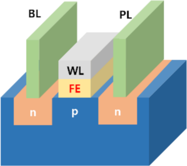
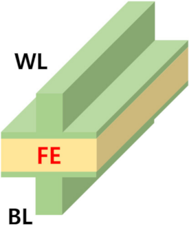
Electrical Characteristics
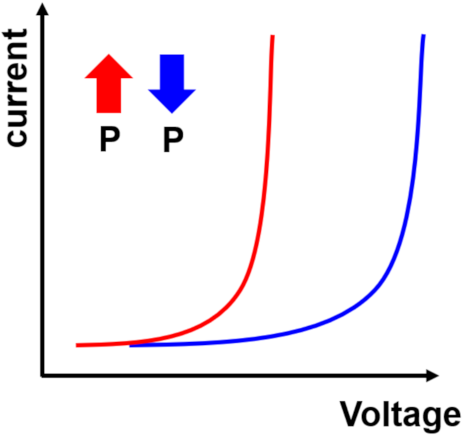
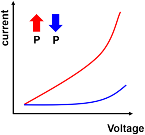
 Electronics 10 02759 i004 Electronics 10 02759 i005 Electronics 10 02759 i006
ReadDestructiveNon-destructiveNon-destructive
Energy/bi~100 fJ~10 fJ~1 pJ
Endurance>1012>1010>107
Cell size30–40 F210–30 F24–8 F2
Cell structure1 T–1 F1 T1 F
Publisher’s Note: MDPI stays neutral with regard to jurisdictional claims in published maps and institutional affiliations.

