Article

A PVT-Insensitive Optimal Phase Noise Point Tracking Bias Calibration in Class-C VCO

School of Electrical Engineering and Computer Science, Gwangju Institute of Science and Technology, Gwangju 61005, Korea
*
Author to whom correspondence should be addressed.
Electronics 2022, 11(4), 629; https://doi.org/10.3390/electronics11040629
Submission received: 28 December 2021 / Revised: 14 February 2022 / Accepted: 15 February 2022 / Published: 17 February 2022
(This article belongs to the Special Issue Mixed Signal Circuit Design)

Abstract

:
This paper presents a Class-C voltage-controlled oscillator (VCO) with bias voltage calibration that automatically finds the low-phase noise point and achieves robust start-up regardless of PVT variation. This VCO structure also has the bias circuit that compensates for temperature changes even when calibration is not applied. Through these techniques, the problems of robust start-up and vulnerability to PVT variation, which are chronic problems of Class-C VCO, are overcome. The proposed VCO was designed in a 28 nm CMOS process. Simulation results show that this VCO has an operating range from 3.717 to 4.675 GHz, resulting in a frequency tuning range (FTR) of 22.8%. In addition, power consumption was 2.135 mW, phase noise at 1 MHz was −124.1 dBc/Hz, and the figure of merit (FoM) was −192.2 dBc/Hz. The chip area was very small at 0.196 mm 2 .

1. Introduction

In transceiver design for wireless communication, one of the key blocks included in the phase-locked loop (PLL) is a voltage-controlled oscillator (VCO). Therefore, optimizing the VCO block is very important as it greatly contributes to improving the overall performance of the transceiver [1]. Recent studies focused on Class-C operation that could improve the performance of VCO, and studies are also frequently conducted to solve problems caused by applying Class-C operation [2,3,4,5,6,7,8,9]. The Class-C operation of an oscillator is implemented by lowering the gate bias voltage by adding an RC network to the MOS cross-coupled pair in the Class-B structure, as shown in Figure 1. There are advantages to Class-C operation. First, the reduced gate voltage bias shows 36% lower power consumption compared to that of Class-B operation [2]. Second, an optimal bias voltage shows better phase noise performance [3], resulting in a superior figure of merit (FoM).
However, there are several problems that need to be solved: (1) the start-up robustness problem due to low bias voltage [5]; and (2) sensitivity to process, supply-voltage, and temperature (PVT) variation. This paper presents solutions to these two problems. First, the proposed algorithm solves the start-up problem using digital calibration and determines the bias voltage appropriate for a given PVT variation. Next, the proposed bias circuit makes it possible to stably maintain Class-C operation against changing temperature.
Attempts to calibrate the bias voltage of Class-B and -C VCOs are steadily ongoing [4,7,8,9,10,11]. Most of these methods use analog and digital feedback loops to put the oscillation amplitude or the voltage of the tail current source within a certain range. This specific range can be changed by the external reference voltage included in the loop, so it is difficult to say that the specific range is determined at the design stage. This is because the range showing the best performance can be adjusted by changing the reference voltage in the measurement step. These methods have limitations in the process variation of chips and are difficult to use for real applications. In addition, the authors in [4,8] included simulation results assuming process variation, showing only transient response showing robust start-up, and did not analyze phase noise with process variations. According to subsequent analysis in this paper, the change in phase noise was very large when PVT variations were given. Therefore, so far, it is difficult to design Class-C VCOs that are actually applicable to the industry while overcoming PVT variations with the calibration method.
Therefore, this work proposes the calibration method of not requiring manual measurement after tape out to find an appropriate reference voltage for optimal phase noise. In this paper, the tendency of phase noise according to bias voltage is analyzed, and an appropriate bias voltage is automatically found by the proposed calibration process.

2. Proposed Circuit Implementation

The entire block diagram of the proposed Class-C VCO system is shown in Figure 1b. The output of the VCO was connected by a peak detector to detect the output amplitude and compare this value with the supply voltage in the comparator. The output of the comparator was connected to the digital calibration block, and the calibration output enters the bias circuit and adjusts the gate bias voltage of the VCO.
In this part, each block in Figure 1b is described in detail. Firstly, the proposed bias circuit is compared with the conventional design and the complementation of the temperature variation of the proposed scheme is explained. Subsequently, we introduce the digital calibration algorithm that implements the robust start-up of Class-C operation and automatically finds the optimal performance bias point without affecting PVT variation. Lastly, several detailed characteristics of this system such as OFF detection scheme are described.

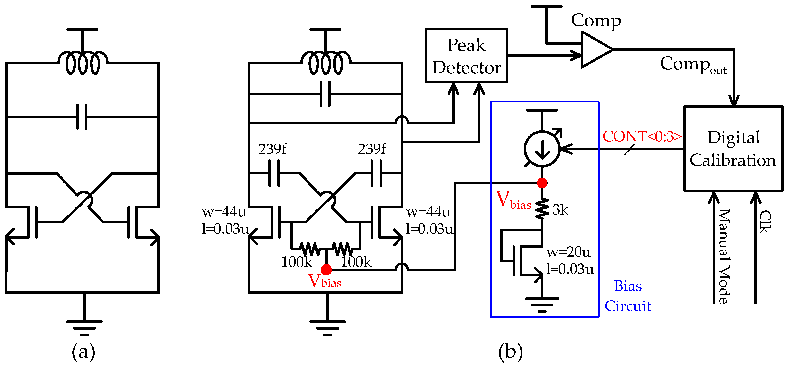
2.1. Bias Circuit for Class-C VCO

2.1.1. Conventional Bias Circuit

For Class-C operation, a robust start-up is typically implemented with a high gate bias voltage for Class-B operation when the oscillation starts, and the bias voltage is dropped to a low voltage to enter the Class-C operation region. In order to properly generate this bias voltage, as shown in Figure 2a, the analog bias circuit of a Class-C oscillator is typically used [6]. This structure can generate a bias voltage that is initially high and then decreases without a certain calibration, as shown in Figure 2b.
However, this conventional structure needs to have the selected current bias to have the Class-C operating bias voltage. As shown in Figure 2b, the settling point of the bias voltage differs by current. By changing just one code of the current, the VCO can be turned off. So, there must be a process to find the appropriate current range that the VCO can operate to avoid the risk of turning off. With this conventional bias circuit, the optimal phase noise point cannot be expected, so finding the current for the optimal point is also needed every time. Moreover, this range and the optimal point are very sensitive to PVT variations. Therefore, the operating current range and the optimal point of the VCO must be checked every time the measuring circumstance changes.

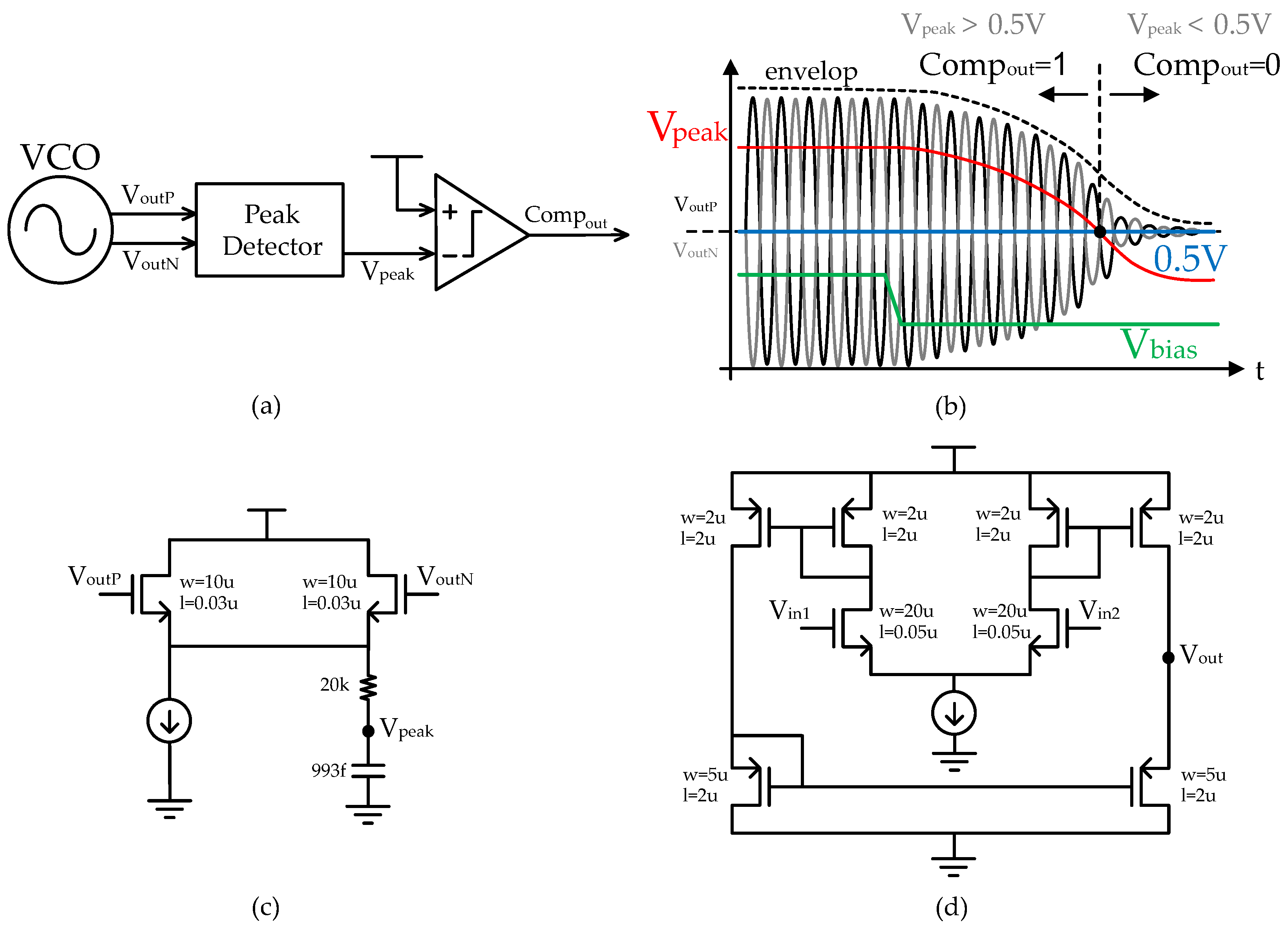
2.1.2. Proposed Bias Circuit

As the conventional structure has the inconvenience of finding the optimal current every time, and some drawbacks such as design complexity and large area due to a large capacitance, we propose a simple bias circuit with digital calibration in Figure 3. This intuitive structure consists of a load part and a current generator, and the current is controlled by proposed bias calibration to provide bias voltage for Class-C operation as shown in Figure 3b. Through the method of adjusting the current with digital calibration, Class-C bias circuit can be implemented that not only eliminates the disadvantages of conventional bias circuit, but also guarantees a robust start-up of Class-C VCO.
As the temperature changes, the threshold voltage of core MOS pair changes. When the threshold voltage of Core MOS changes rapidly, VCO can be turned off when it operates in the Class-C region. For example, since the threshold voltage is low at high temperature, suppose that a low bias voltage for Class-C operation is applied accordingly. If the temperature drops rapidly in this state, the threshold voltage of the MOS increases, and the VCO may be turned off. Therefore, if the bias voltage tracks as the threshold voltage changes, the overdrive voltage of the Core MOS is maintained, thus preventing the VCO from turning off.
To generate the bias voltage that tracks the threshold voltage, the load part consisted of a resistor and diode-connected MOS, as shown in Figure 3a. The diode-connected MOS was designed in a constant ratio with that of VCO Core, which compensated for the temperature variation of VCO. Referring to Equation (1), V T H increases when the temperature decreases.
V T H = V T H 0 + γ ( 2 Φ F + V S B Φ F ) , Φ F = ( k T q ) l n ( N A n i )
I D S = 1 2 μ n C o x W L ( V G S V T H ) 2 = 1 2 μ n C o x W L V O V 2
At this time, the V T H of the load MOS also increases. When referring to Equation (2), if V T H of the load MOS increases while the current is fixed, V G S increases. Therefore, as V T H increases, V b i a s increases. Therefore, from the point of view of the core MOS, the overdrive voltage is maintained, so it does not deviate from the existing operational region.
Figure 4 shows the threshold voltage and bias voltage of the core MOS according to temperature change. The proposed load model in Figure 3a applied to the structure of this paper and the resistor-only load model as shown in the same figure were compared and plotted. The resistance value of the resistor-only model was set to have the same bias voltage as the proposed model at 27 °C. Figure 4b compares the overdrive voltage of the Core MOS of the two models. When −40 °C and 125 °C are compared, the amount of change of the overdrive voltage in the proposed model is 26.76 mV, whereas the amount of change in the overdrive voltage of the resistor only model is 92.94 mV. In the case of the proposed model, the amount of change in overdrive voltage was reduced by 71%.

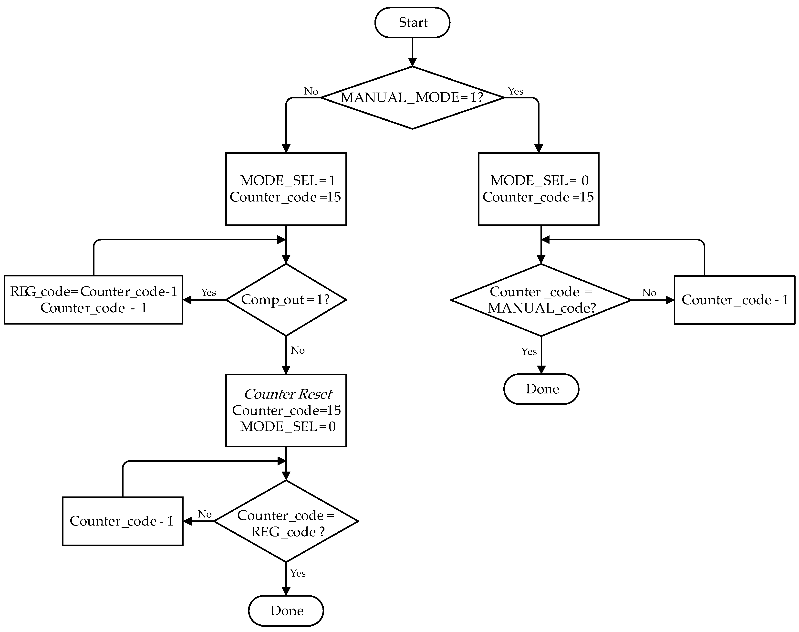
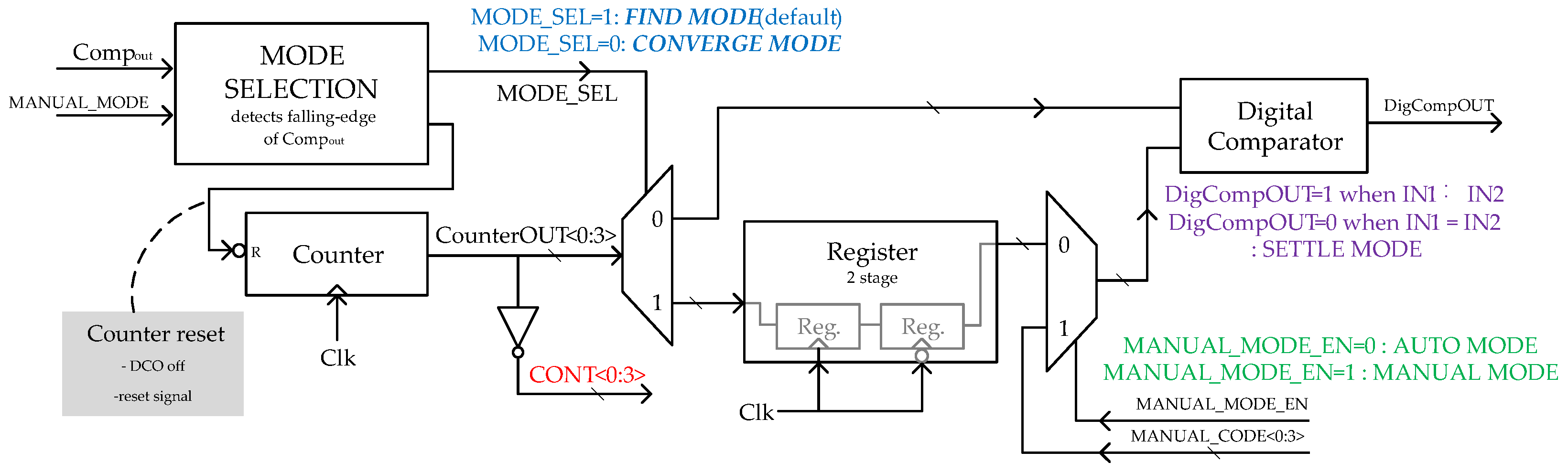
2.2. Proposed Algorithm for Digital Calibration

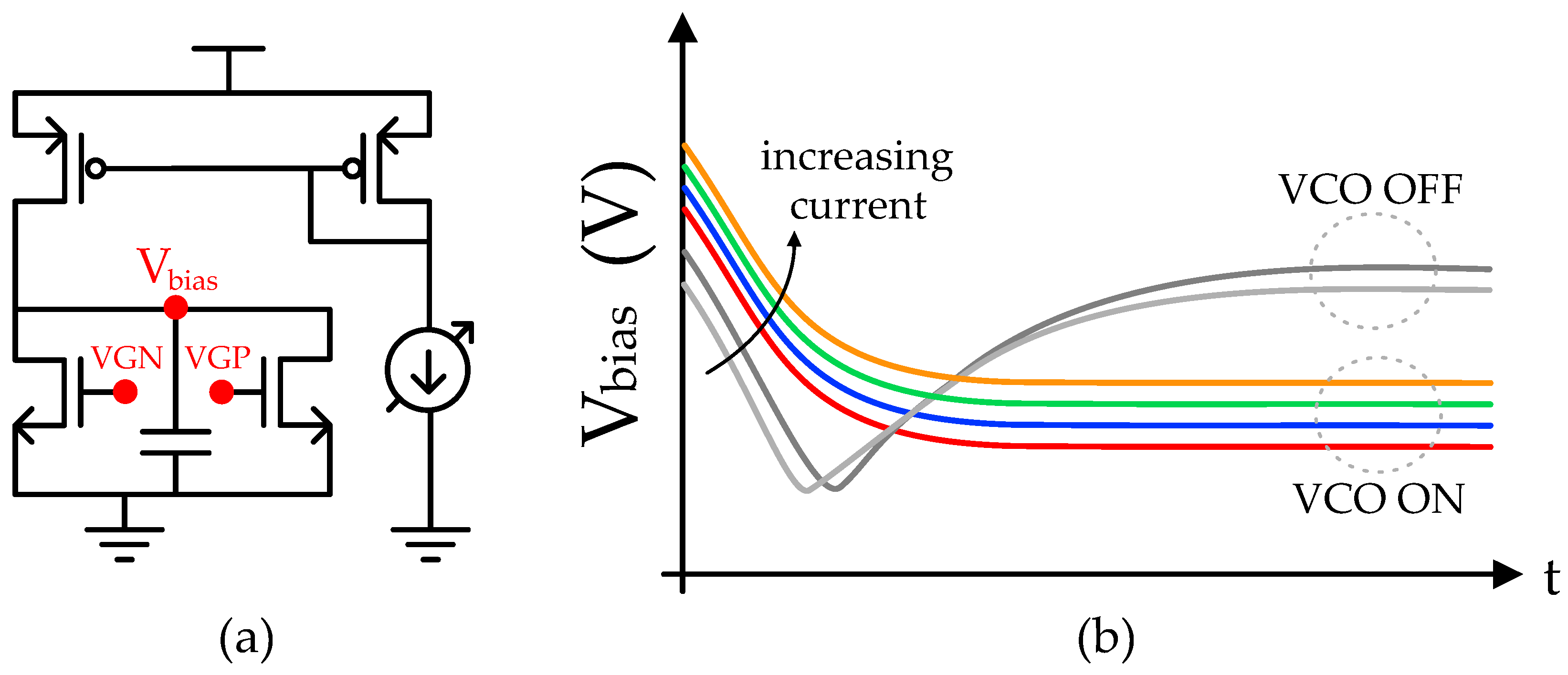
2.2.1. Tendency of Phase Noise According to Bias Voltage

In order to find the optimal bias level regardless of PVT variation, we plotted the phase noise for bias voltage as shown in Figure 5. PVT variation was assumed in this way: process variation (nn, ff, ss), ±10% supply voltage variations (0.45, 0.5, and 0.55 V), and temperature variation (−40, 27, and 125 °C) were plotted for 9 cases.
In all cases, there was a similar trend. The lower the bias level code was, the lower the bias voltage level. In all cases, the lower the bias voltage was, the more the phase noise tended to improve. If the bias voltage became too low, the VCO did not operate and turned off. On average, it showed the best phase noise at the 2–3 codes before the turn-off code. For example, in Figure 5, the blue graph was the case of the nn corner, 27 °C, and 0.5 V, and it operated up to code level 7 because VCO turned off at code level 6. In this case, the optimal point showing the best phase noise performance is code level 8 and it can be seen that it is before 2 codes from the OFF point of code level 6. When analyzing the optimal point in this way, each had a different optimal code.
As analyzed above, PVT variation is severe for VCOs operating in Class-C, and a different bias voltage is required according to each situation. In [4,8,9], regarding the bias control of Class-C VCO, the optimal bias voltage was found using a specific reference voltage level from the outside. In order for a circuit to actually be used, it is difficult to find an optimal point in a different situation each time. Therefore, we tried to construct an algorithm, so that the circuit could adjust the bias voltage close to the optimal point by itself in a given situation. Figure 5 shows that the bias voltage of the oscillator showed the best phase noise just before it was turned off. Using this, the algorithm was configured to detect the bias point where VCO was off and to converge near the off point. The transient response plot of VCO to which this algorithm was applied is shown in Figure 6.

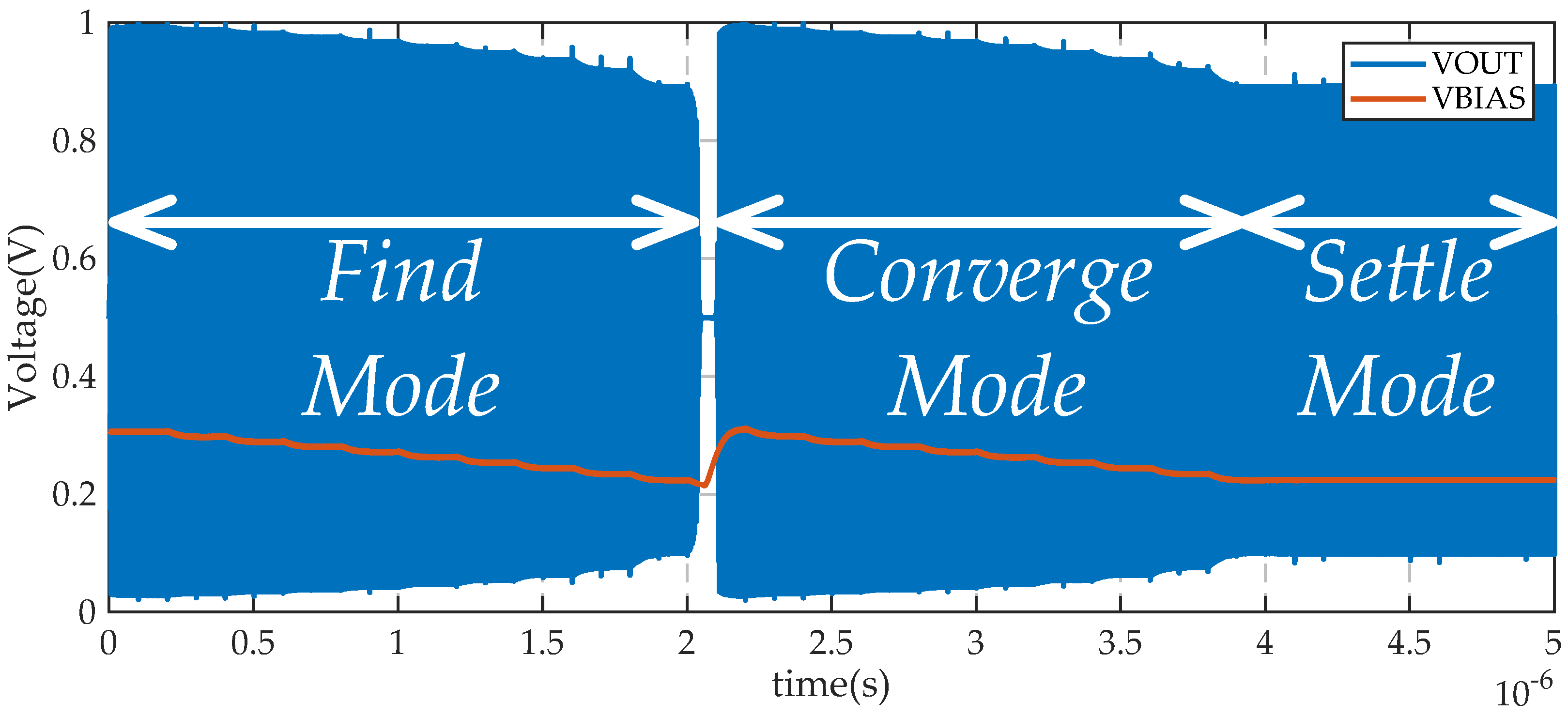
2.2.2. Bias Calibration Algorithm

In Figure 6, the red line is the transient response of the bias voltage and the green line is the VCO output node voltage. This algorithm is largely divided into three modes. First, in Find   mode , the optimal point is found and stored in the register. Second, in Converge   mode , the bias level converges with the stored optimal point. Lastly, when the stored optimal point and the bias level are the same, the bias level no longer changes and goes into Settle   mode .
In Find   mode , the initial bias level begins with a maximal point. The bias level is lowered one by one to detect the operating state of the VCO and reflect it in the adjustment of the bias level. If the VCO maintains ON operation for a specified time, the bias level is lowered by one step. However, if the VCO fails to operate and turns OFF, the bias level is reset to the maximal point. When the VCO is in the ON state in Find mode, the code indicating the bias level is stored in the register. Therefore, it is stored up to the code just before it is turned off, and this is referred to as an optimal code.
In Converge   mode , the bias level converges to the stored optimal code. As VCO OFF was detected and Find mode ends, the bias level was reset to the maximal point. Therefore, the VCO begins to operate again. As in Find   mode , the bias level goes down one code at a time. However, unlike Find Mode, in Converge Mode, the bias code is not stored in the register. On the other hand, it compares the already stored optimal code and bias code in real-time, and the bias code continues to go down until these two codes are the same, and when they are the same, the bias level is no longer changed and fixed. This is the Settle   mode .
Figure 7 shows the creation of the above bias calibration concept as a flow chart. Figure 8 is the structure of a digital block designed x on the basis of the flow chart. This calibration block consists of the counter, register, Mode Selection block, digital comparator, MUX, and DEMUX. The counter is reset when the VCO is OFF or the external reset signal is applied. Along with the clock signal, the counter makes the bias codes for the bias circuit, which is represented as CONTS<0:3> in the figure. The Mode Selection block detects the falling edge of the comparator output which means the ON/OFF state of the oscillator. From this information, the Mode Selection block distinguishes whether the current calibration state is Find   mode or Converge   mode . When it is Find   mode , the counter output is saved at the register and when it is in the Converge   mode , the saved code is compared to the counter output until these two codes are equal. This comparison process is conducted at the digital comparator block. When the counter output becomes equal to the saved codes, the output of the digital comparator stops the clock signal of the whole calibration block.

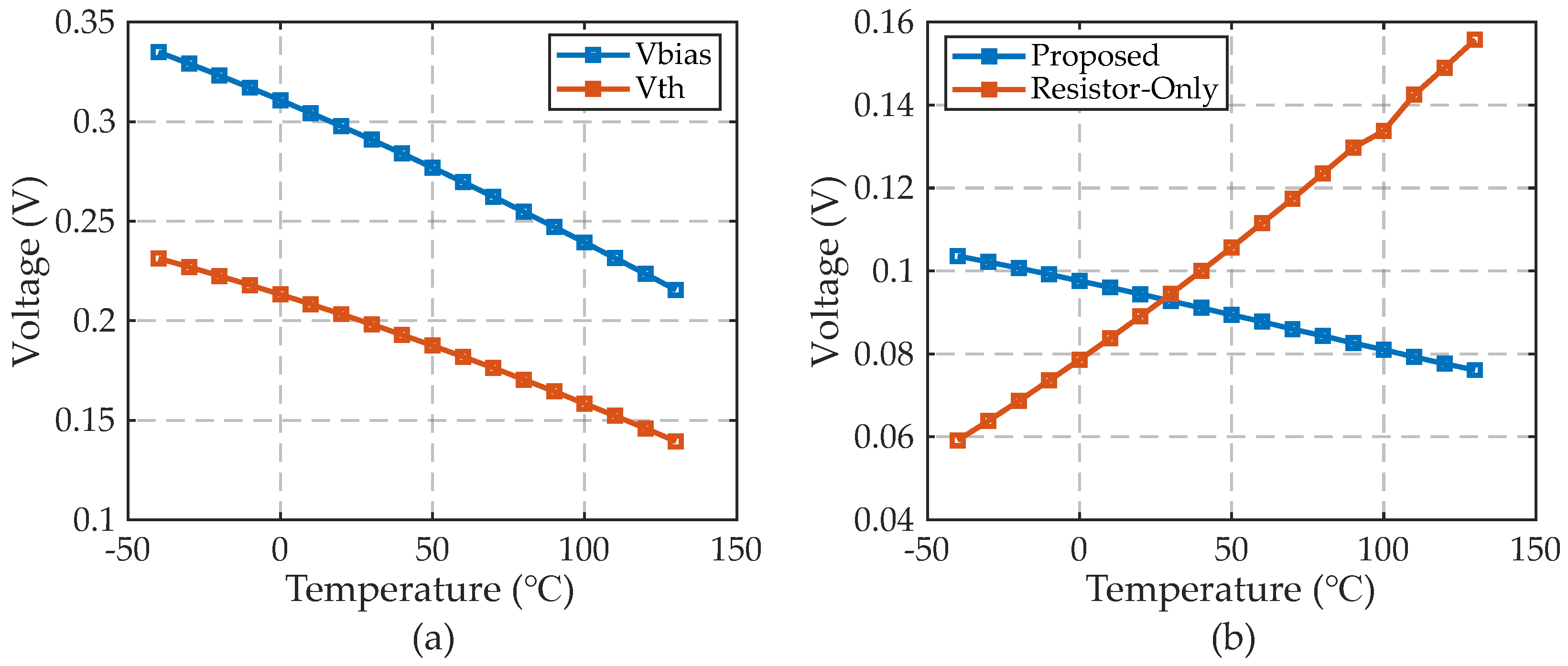
2.2.3. Detailed Characteristics

  • Bias Level Control Method
As mentioned, it is necessary to lower the bias level one by one in Find   mode . As shown in Figure 3a, the bias circuit of the designed VCO consists of the current generator and load. The current generator receives 4-bit binary code and generates a current change amount proportional to it. The bias level is changed by the 4-bit binary code, which is the input of the current generator.
Therefore, this 4-bit binary code is generated by the counter. (Figure 8) The counter output was lowered by one code by a clock signal. The counter contains a reset. If VCO is OFF or an external reset signal is entered, the bias code is reset to the maximum code again. In addition, when the interval code and counter output are the same in Converge mode, the counter clock stops.
  • VCO OFF Detection
The most important function in Find   Mode is VCO OFF detection. The ON/OFF state of VCO should be recognized and expressed in digital code. When the VCO is turned off, the swing decreases rapidly. The rapid change in the swing level may be detected using a peak detector and a comparator [12]. The circuit for OFF detection and its transient response is shown in Figure 9. To this end, VCO output is received as a peak detector, which detects the envelope of the swing of VCO oscillation swing. V p e a k signal is compared to the reference voltage, which was set to 500 mV in this paper. This reference voltage is connected to the supply voltage. This value is designated as a value that can determine ON/OFF on the basis of the value of V p e a k through simulation. When PVT variations are given, this value may change. However, this change is insignificant, so there is no problem in catching the rapid change in V p e a k . Then C o m p o u t signal expresses the ON/OFF status of VCO as 1 and 0. Using this C o m p o u t value, transition from Find   Mode to Converge   Mode is possible.
  • Manual Mode
Figure 8 shows that the manual mode was added as an option to this calibration. Class-C operation has the advantage of low power consumption, but manual mode can be used if operating at a bias level is preferred to more robust operation or a code by calibration. Auto Mode was named when the above-described calibration was used as it is, not in manual mode.
In Manual Mode, since it converges to the Manual Code entered from the outside, Find Mode is omitted and immediately enters Converge Mode. In the existing calibration, it converged to the code stored in the register, but in Manual Mode, the manual code is input to the input of the digital computer. If Class-C operation is not necessary, this manual mode option can be used.

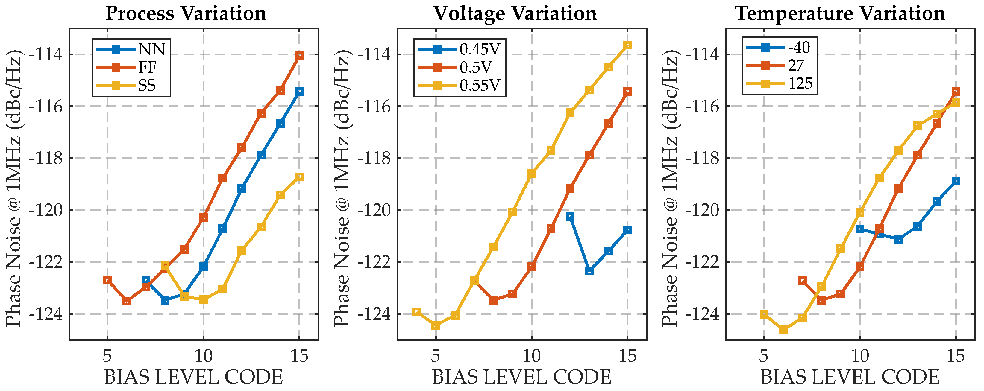
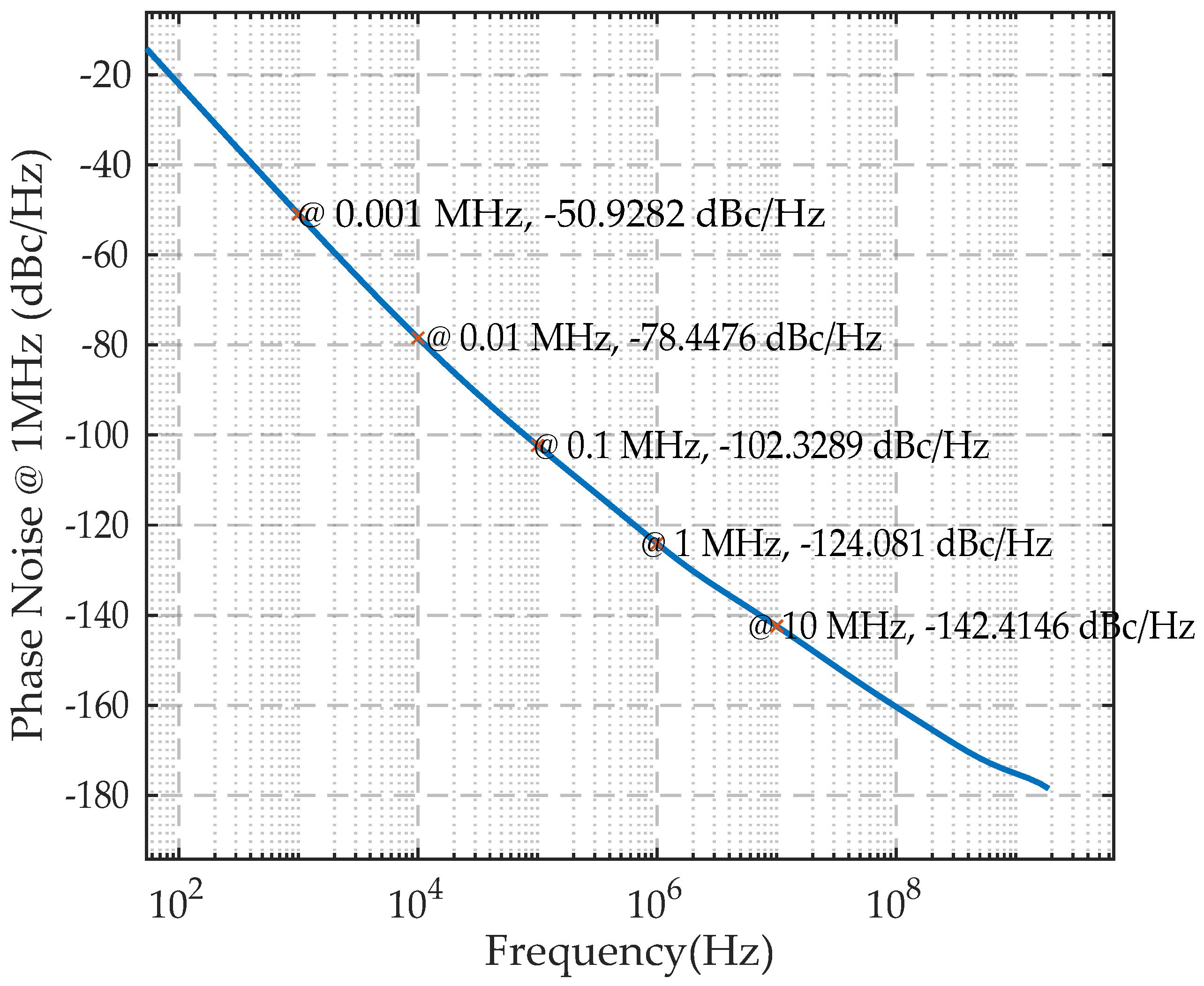
3. Simulation Results

Class-C VCO and calibration block introduced in this paper were designed as Samsung 28 nm CMOS process. The simulated Q value of the inductor used in this VCO for optimal phase noise is 16.6. The layout design is shown in Figure 10a. The area of VCO that is composed of the inductor, capacitor banks, oscillator core, calibration block, current generator for calibration block, and the output buffer is 0.45 × 0.43 mm 2 . This VCO is included in the Phase-Locked Loop (PLL), and the entire layout design can be seen in Figure 10b. According to the post-layout simulation result, the tuning range of the proposed VCO at NN corner was 3.717 at 4.675 GHz. In each case, the power consumption was 2.135 and 1.966 mW. When the output frequency is 3.717 GHz in the NN corner, the phase noise plot is shown in Figure 11. Phase noise was −124.1 dBc/Hz at 1 MHz offset frequency and −142.4 dBc/Hz at 10 MHz. Accordingly, F o M and F o M T can be calculated as in Equations (3) and (4). At 1 MHz offset frequency, F o M is −192.2 dBc/Hz and F o M T is −199.4 dBc/Hz.
F o M = P N 20 log 10 ( f 0 Δ f ) + 10 log 10 ( P D C 1 m W )
F o M T = P N 20 log 10 ( f 0 Δ f ) + 10 log 10 ( P D C 1 m W ) 20 log 10 ( T R 10 )
In addition, Figure 12 shows the transient simulation results of bias voltages of the VCO with bias calibration with 7 corner variations (NN, FF, SS, 125 °C, −40 °C, 0.55 V, 0.45 V) applied, and bias calibration operated well in each corner. The start-up time of this VCO was less than 10 ns. The entire calibration loop time differs by PVT variations, but the time was less than 5 μ s in all cases. As a result, all cases with PVT variations were starting up well.
Table 1 compares the characteristics of the calibration scheme with other papers suggesting the bias voltage calibration of Class-C VCO. All reference papers calibrate VCO’s output amplitude through the feedback loop, and all use the external reference voltages within that feedback, which means that the external voltages can be modified during the measurement process. These works focus on ensuring the robust start-up of Class-C operation through amplitude feedback. However, most studies do not include the ways to overcome PVT variations within the calibration design stage. Therefore, this study is meaningful in that it is equally applicable in all situations of PVT variations and it is the only calibration method that tracks the optimal bias point.
Performance comparison table is shown in Table 2. Compared to [14], the proposed calibration resulted in better F o M , F o M T at the 1 M offset frequency, but the tuning range is slightly worse than that of [14] because of the degraded on/off tank capacitor ratio, which would have been improved by a better layout. The simulated Q value of our inductor was 16.6, which was lower than the 18 in [14]. Higher Q would result in better phase noise according to [15].

4. Conclusions

In this paper, a 4 GHz Class-C VCO was implemented with digital bias calibration to optimize the bias voltage and bias circuit load model compensating the temperature changes. Through this structure, it was possible to solve the start-up robustness problem and the sensitivity to PVT variations, which are problems in the Class-C operation of VCO. It was possible to detect the OFF point of VCO through bias calibration and automatically track to the low phase noise point by aligning the bias level near the OFF point. The optimal phase noise point was different depending on the PVT variation, and this calibration method allowed for finding the bias level suitable for the PVT situation. In addition, more stable oscillation can be continued by applying the bias circuit load model that can respond to temperature changes even when the bias voltage is fixed after calibration. Post-layout simulation confirmed that when corner variations are given, it works as designed by bias calibration. The proposed VCO had a turning range from 3.717 to 4.675 GHz and a TR value of 22.8%. Power consumption was 2.135 mW. When the offset frequency was 1 MHz, phase noise is −124.1 dBc/Hz, and F o M is −192.2 dBc/Hz. The area of the VCO block is 0.45 × 0.43 mm 2 . The proposed VCO was designed with Samsung 28 nm CMOS.

Author Contributions

Conceptualization, G.J., S.S. and M.L.; methodology, G.J.; validation, G.J.; formal analysis, G.J.; investigation, G.J. and S.S.; data curation, G.J.; writing—Original draft preparation, G.J.; writing—Review and editing, G.J.; visualization, G.J.; supervision, M.L.; project administration, M.L.; funding acquisition, M.L. All authors have read and agreed to the published version of the manuscript.

Funding

This work was supported by the Commercializations Promotion Agency for R&D Outcomes (COMPA) grant funded by the Korean government (MSIT) (No.2021I100) This work was also supported in part by Samsung Electronics Co., Ltd. The EDA Tool was supported by the IC Design Education Center.

Data Availability Statement

All the data are reported/cited in the paper.

Acknowledgments

This work was supported by the Commercializations= Promotion Agency for R&D Outcomes(COMPA) grant funded by the Korean government (MSIT) (No.2021I100) This work was also supported in part by Samsung Electronics Co., Ltd. The EDA Tool was supported by the IC Design Education Center.

Conflicts of Interest

The authors declare no conflict of interest.

References

  1. Xie, J.; Vamshi, M.K.; Do, M.A.; Boon, C.C.; Yeo, K.S. A low power low phase noise dual-band multiphase VCO. Microelectron. J. 2012, 43, 1016–1022. [Google Scholar] [CrossRef]
  2. Fanori, L.; Andreani, P. Highly Efficient Class-C CMOS VCOs, Including a Comparison with Class-B VCOs. IEEE J. Solid-State Circuits 2013, 48, 1730–1740. [Google Scholar] [CrossRef]
  3. Hu, Y.; Siriburanon, T.; Staszewski, R.B. Intuitive Understanding of Flicker Noise Reduction via Narrowing of Conduction Angle in Voltage-Biased Oscillators. IEEE Trans. Circuits Syst. II Express Briefs 2019, 66, 1962–1966. [Google Scholar] [CrossRef] [Green Version]
  4. Liao, X.; Liu, L. A Low-Voltage Robust Class-C VCO With Dual Digital Feedback Loops. IEEE Trans. Circuits Syst. II Express Briefs 2020, 67, 2347–2351. [Google Scholar] [CrossRef]
  5. Mazzanti, A.; Andreani, P. Class-C Harmonic CMOS VCOs, With a General Result on Phase Noise. IEEE J. Solid-State Circuits 2008, 43, 2716–2729. [Google Scholar] [CrossRef]
  6. Tohidian, M.; Fotowat-Ahmadi, A.; Kamarei, M.; Ndagijimana, F. High-swing class-C VCO. In Proceedings of the 2011 Proceedings of the ESSCIRC (ESSCIRC), Helsinki, Finland, 12–16 September 2011; pp. 495–498. [Google Scholar] [CrossRef]
  7. Xu, X.; Yang, X.; Yoshimasu, T. 2.4-GHz band low-voltage class-C PMOS VCO IC with amplitude feedback loop. In Proceedings of the 2015 Asia-Pacific Microwave Conference (APMC), Nanjing, China, 6–9 December 2015; Volume 3, pp. 1–3. [Google Scholar] [CrossRef]
  8. Yang, X.; Xu, X.; Yoshimasu, T. An ultra-low-voltage Class-C PMOS VCO IC with PVT compensation in 180-nm CMOS. In Proceedings of the 2016 IEEE 16th Topical Meeting on Silicon Monolithic Integrated Circuits in RF Systems (SiRF), Austin, TX, USA, 24–27 January 2016; pp. 107–109. [Google Scholar]
  9. Zhu, Z.; Liang, L.; Yang, Y. A Startup Robust Feedback Class-C VCO With Constant Amplitude Control in 0.18 μm CMOS. IEEE Microw. Wirel. Compon. Lett. 2015, 25, 541–543. [Google Scholar] [CrossRef]
  10. Zhang, Y.; Boon, C.C.; Miao, Y.; Do, M.A.; Yeo, K.S. Novel hybrid type Automatic Amplitude Control loop VCO. In Proceedings of the 2011 International Conference on Electronics, Communications and Control (ICECC), Ningbo, China, 9–11 September 2011; pp. 356–359. [Google Scholar] [CrossRef]
  11. Jia, L.; Ma, J.G.; Yeo, K.S.; Yu, X.P.; Do, M.A.; Lim, W.M. A 1.8-V 2.4/5.15-GHz dual-band LCVCO in 0.18-μm CMOS technology. IEEE Microw. Wirel. Compon. Lett. 2006, 16, 194–196. [Google Scholar] [CrossRef]
  12. Chen, J.; Jonsson, F.; Carlsson, M.; Hedenas, C.; Zheng, L.R. A Low Power, Startup Ensured and Constant Amplitude Class-C VCO in 0.18 μm CMOS. IEEE Microw. Wirel. Compon. Lett. 2011, 21, 427–429. [Google Scholar] [CrossRef]
  13. Deng, W.; Okada, K.; Matsuzawa, A. Class-C VCO With Amplitude Feedback Loop for Robust Start-Up and Enhanced Oscillation Swing. IEEE J. Solid-State Circuits 2013, 48, 429–440. [Google Scholar] [CrossRef]
  14. Murphy, D.; Darabi, H.; Wu, H. Implicit Common-Mode Resonance in LC Oscillators. IEEE J. Solid-State Circuits 2017, 52, 812–821. [Google Scholar] [CrossRef]
  15. Hajimiri, A.; Lee, T. A general theory of phase noise in electrical oscillators. IEEE J. Solid-State Circuits 1998, 33, 179–194. [Google Scholar] [CrossRef] [Green Version]
  16. Perticaroli, S.; Dal Toso, S.; Palma, F. A Harmonic Class-C CMOS VCO-Based on Low Frequency Feedback Loop: Theoretical Analysis and Experimental Results. IEEE Trans. Circuits Syst. I Regul. Pap. 2014, 61, 2537–2549. [Google Scholar] [CrossRef]
Figure 1. (a) VCO structure for Class-B operation; (b) entire block diagram of proposed Class-C VCO system.
Electronics 11 00629 g001
Figure 2. (a) Conventional structure of bias circuit for Class-C VCO and (b) its transient response of bias voltage for different current levels.
Electronics 11 00629 g002
Figure 3. (a) Proposed bias circuit and resistor load model for comparison. (b) Modeling of digital calibration for Class-C VCO bias voltage.
Electronics 11 00629 g003
Figure 4. (a) Bias voltage tracking threshold voltage in proposed bias circuit and (b) overdrive voltages according to temperature.
Electronics 11 00629 g004
Figure 5. Tendency of phase noise according to bias voltage with process, voltage and temperature variations.
Electronics 11 00629 g005
Figure 6. Transient response of VCO with bias calibration.
Electronics 11 00629 g006
Figure 7. Flow chart of proposed bias calibration algorithm.
Electronics 11 00629 g007
Figure 8. Bias calibration block diagram.
Electronics 11 00629 g008
Figure 9. (a) Block diagram of OFF detection circuit, (b) its transient response detecting the OFF state of the oscillator, (c) structure of peak detector, and (d) comparator.
Electronics 11 00629 g009
Figure 10. Layout design of (a) proposed VCO block and (b) entire PLL block including VCO block.
Electronics 11 00629 g010
Figure 11. Post-layout simulation phase noise at NN corner and 3.717 GHz output frequency.
Electronics 11 00629 g011
Figure 12. Post-layout simulation transient response of bias voltage in NN, FF, SS, 125 °C, −40 °C corners.
Electronics 11 00629 g012
Table 1. Comparison of characteristics of bias calibration for Class-C VCO.
Proposed[4][12][13][8][9]
Calibration MethodDigitalDigitalDigitalAnalogAnalogAnalog
External reference voltagesXOOOOO
Number of calibration loops121112
Optimal phase noise trackingOXXXXX
Table 2. Performance comparison table among recently published state-of-art CMOS VCOs.
Proposed *[16][12][14][6][2][11]
Tech.28 nm55 nm180 nm28 nm180 nm90 nm180 nm
Config.Class-CClass-CClass-CClass-BClass-CClass-CClass-B
Supply
Voltage (V)
0.51.51.00.91.21.21.5
Tuning
Range (GHz)
3.717–4.6756.5–7.82.6–3.12.85–3.754.84 (N.A.)3.4–4.52.2–2.85
/4.4–5.7
TR(%)22.818.22027.3N.A. **2825.7/25.7
Phase Noise
@1 MHz
(dBc/Hz)
−124.1−127−123.0−131−125−127 ***−110 ***/ −97 ***
F o M
(dBc/Hz)
−192.2@1 MHz
−205.3@5 MHz
−187
@1 MHz
−191.1
@1 MHz
−192
@5 MHz
−193
@1 MHz
−191
@1 MHz
−188.3
/−183.7
@3 MHz
F o M T
(dBc/Hz)
−199.4@1 MHz
−212.5@5 MHz
−192.2
@1 MHz
−197.1
@1 MHz
−200.7
@5 MHz
N.A. **−199.9
@5 MHz
−196.5
/−191.9
@3 MHz
P D C (mW)2.135–1.966181.576.63.46.65.4/8
Area (mm 2 )0.1960.4590.770.190.1470.080.04
* Post-layout simulation results. ** Not announced. *** Approximated from the graph.
Publisher’s Note: MDPI stays neutral with regard to jurisdictional claims in published maps and institutional affiliations.

