Article

A 0.17 pJ/bit 28 Gb/s/pin Single-Ended PAM-4 Transmitter for On-Chip Short-Reach Unterminated Channels

Department of Electrical and Electronics Engineering, Konkuk University, Seoul 05029, Korea
*
Author to whom correspondence should be addressed.
Electronics 2022, 11(16), 2525; https://doi.org/10.3390/electronics11162525
Submission received: 25 July 2022 / Revised: 8 August 2022 / Accepted: 9 August 2022 / Published: 12 August 2022
(This article belongs to the Special Issue Mixed Signal Circuit Design)

Abstract

:
This paper presents the design of a single-ended four-level pulse-amplitude modulation (PAM-4) transmitter for an on-chip short-reach unterminated channel. To achieve multi-output generation, a local voltage buffer consisting of a diode-connected device and a leaker transistor is introduced. By charge-sharing between a local reservoir capacitor and an unterminated channel, the proposed transmitter generates mid-level output voltages without using the DC current, thereby realizing multi-level signaling without significantly increasing the static current. A prototype chip was fabricated by 28 nm CMOS process, and the transmitter exhibits an energy efficiency of 0.17 pJ/bit at 28 Gb/s/pin, which is state-of-the-art energy efficiency as a multi-level transmitter having a data rate beyond 20 Gb/s.

1. Introduction

The advent of data-intensive applications such as artificial intelligence (AI) and cloud services requires huge amount of data processing between processors and memories. In such massively parallel memory–processor interfaces, a single-ended link is a preferred electrical interface because reducing the pin count is the most compelling system constraint. A few such examples are the dynamic random access memory (DRAM) interface and high bandwidth memory (HBM) interface. In addition, a short-reach chip-to-chip “chiplet” interface such as bunch-of-wires (BoW) also adopts a single-ended link as a physical layer.
In high-speed single-ended links, a primary design objective is to maximize the data transfer rate per pin while minimizing the energy cost to transfer the bit. Traditionally, increasing the data rate means reducing the bit time, or equivalently increasing the symbol frequency, in combination with mild channel equalization. However, recent developments [1,2] demonstrated the possibility of using multi-level signaling for single-ended links, which allows us to increase the data rate without reducing the bit time. For instance, the authors in [1] demonstrated 22 Gb/s/pin for a single-ended GDDR6X interface using four-level pulse-amplitude modulation (PAM-4) signaling scheme, where a source series termination (SST) voltage-mode structure is used as a transmitter. In [3,4], a pseudo-open-drain logic (PODL) transmitter generates a PAM-4 signal by adjusting the resistance value in the driver.
One challenge of using multi-level signaling is minimizing the energy cost. Specifically, generating mid-level outputs in both SST and PODL structures relies on resistive voltage dividers. Considering the impedance matching with channel impedance, this approach inevitably consumes a large amount of static current when generating mid-level outputs. Accordingly, the energy cost of a previously published single-ended PAM-4 transmitter is generally higher than a binary transmitter, e.g., approximately 1 pJ/bit for 12 Gb/s [5] and 3.1 pJ/bit for 18 Gb/s [3].
This paper presents a low-power 28 Gb/s/pin PAM-4 transmitter optimized for an on-chip short-reach unterminated channel, achieving an energy efficiency of 0.17 pJ/bit. The proposed PAM-4 transmitter generates mid-level outputs using capacitive charge sharing rather than resistive division, leading to substantial power saving. While the use of a capacitive-coupled nonreturn-to-zero (NRZ) driver without termination resistance has been subject of a previous publication [6], such structures are not compatible with the generation of multi-level outputs. In contrast, our proposed transmitter structure overcomes such limitations and achieves both a low energy cost and multi-level generations for unterminated channels.
This paper is organized as follows. Section 2 describes the architecture of the transmitter. Section 3 presents the concept and transistor-level design of the proposed transmitter circuit. The measured performance is shown in Section 4. Section 5 concludes the paper with summary.

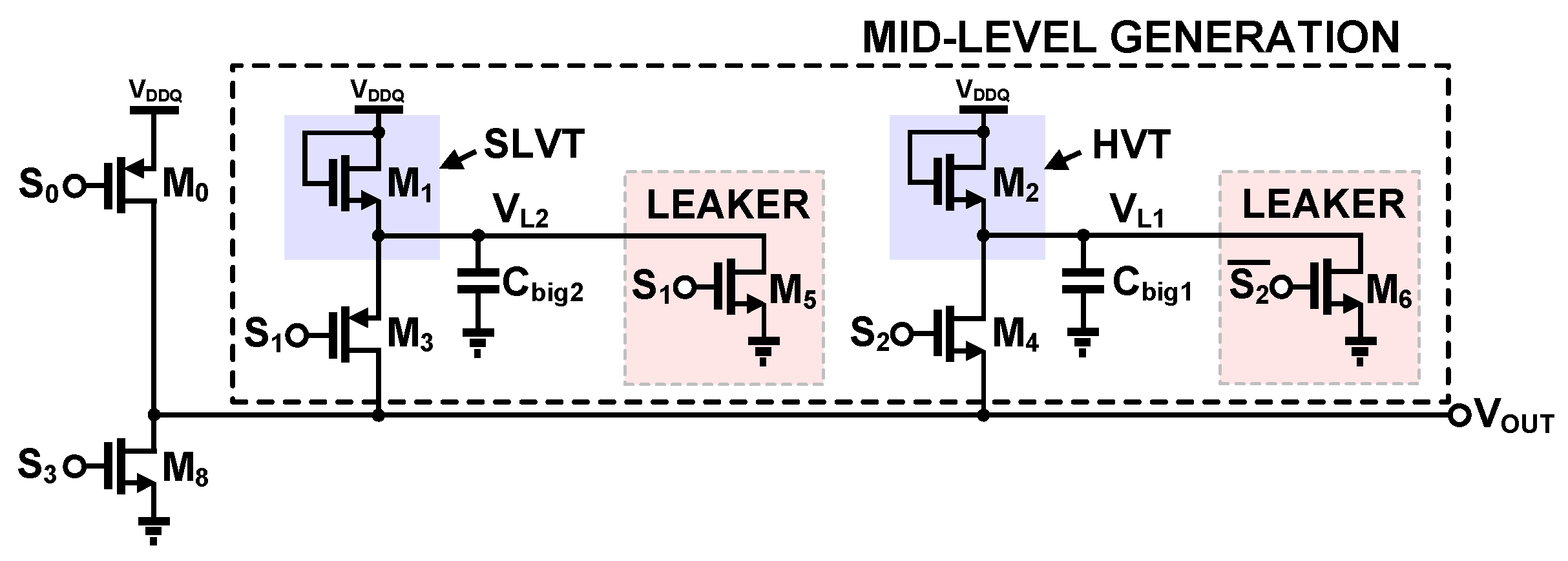
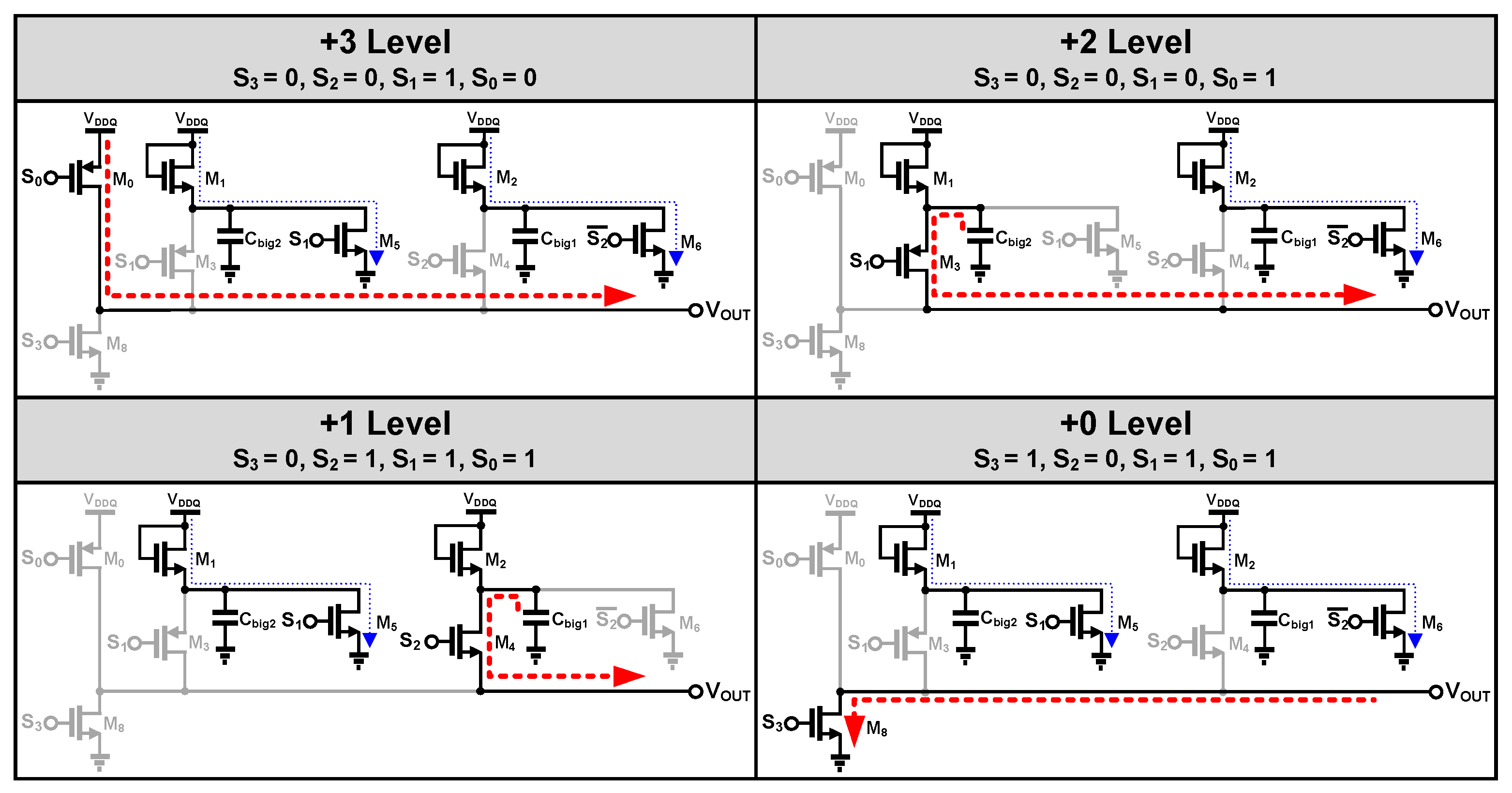
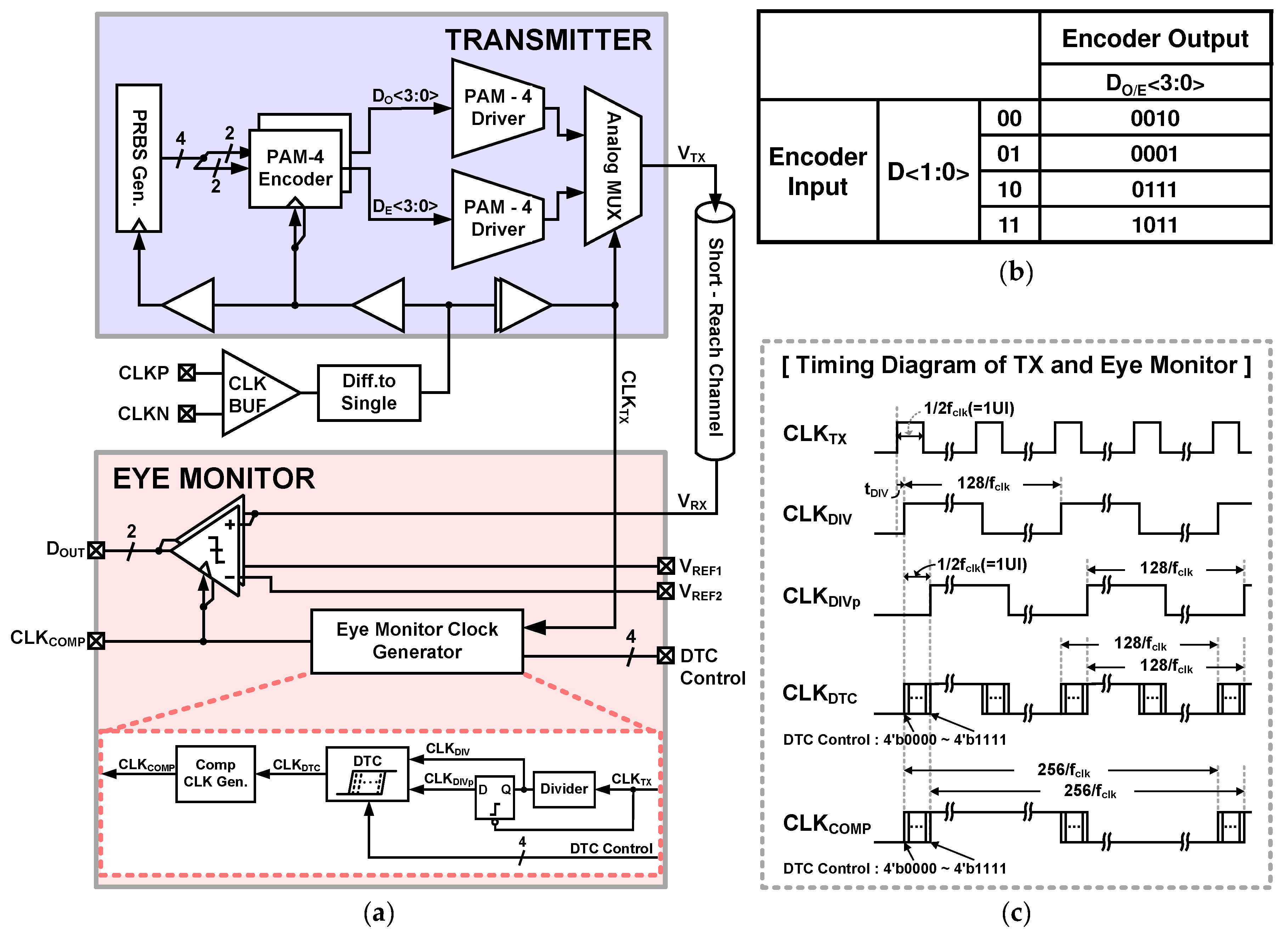
2. Transmitter Architecture

Figure 1a shows the block diagram of the proposed transmitter along with an embedded eye monitor for measuring the on-chip eye diagram. The transmitter consists of a 2 7 1 pseudo random binary sequence (PRBS) generator, a PAM-4 encoder, two PAM-4 drivers and a 2-to-1 analog multiplexer (MUX). The PRBS generator drives the PAM-4 encoder with 4-bit-wide random digital bits, producing a pair of 4-bit-wide bitstream DE<3:0> and DO<3:0>.
The PAM-4 encoder, whose encoding table is shown in Figure 1b, is constructed to control the switches in the transmitter in such a way that four distinct levels are generated. The two bitstreams from the encoders are synchronized at both the rising and the falling edge of CLKTX, respectively, and drive respective PAM-4 drivers. The generated two output voltages are then directly multiplexed by the analog MUX, producing 28 Gb/s PAM-4 signal at VTX when CLKTX is 7 GHz.
The eye monitor, shown in the red box in Figure 1a, consists of two comparators and a clock generator which includes a frequency divider, a 4-bit digital-to-time converter (DTC) and a comparator clock generator. The timing diagram for the DTC and comparators are illustrated in Figure 1c. The DTC is designed to have a full-scale range of 1 unit-interval (UI) by interpolating the CLKDIV and the CLKDIVp, where the CLKDIVp is the delayed CLKDIV synchronized at the falling edges of CLKTX. Two comparators generate outputs by comparing the received voltage VRX with the respective reference voltages, VREF1 and VREF2, where a constant offset is applied for the two references, i.e., VREF2 = VREF1 + VOS. The comparator runs at fclk/256 so that the metastability error of the comparator is negligible. To obtain the eye diagram, the outputs of two comparators are collected while sweeping both the reference voltages and the DTC control bits. Afterwards, a two-dimensional histogram of the VRX is created by post-processing the distribution of the outputs.

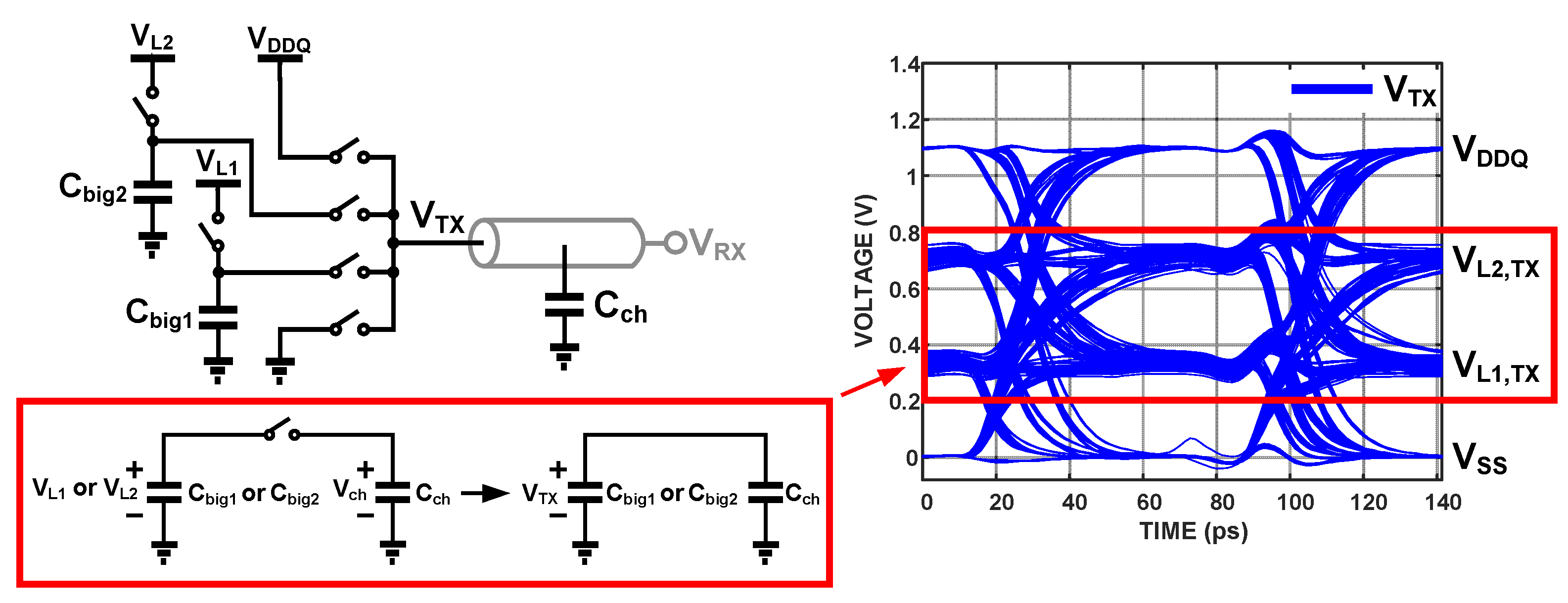
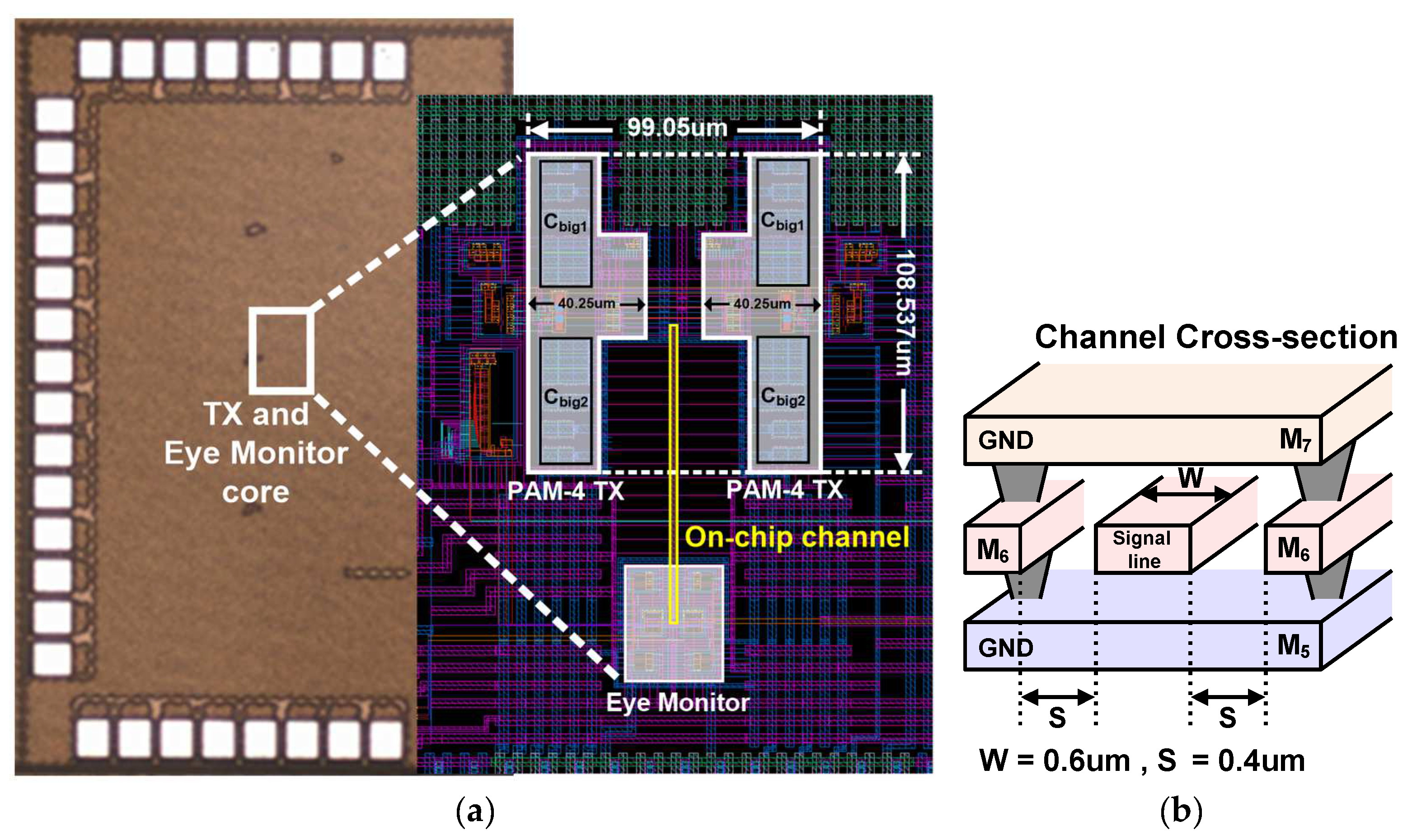
3. Circuit Implementation

Figure 2 shows a transistor-level circuit diagram of the PAM-4 driver that generates four-level outputs, i.e., VDDQ, VL2, VL1 and VSS. The highest and lowest levels are generated by turning on M0 and M8, respectively, which is essentially same as SST drivers. The key difference is generating mid-level outputs, VL1 and VL2. Unlike the SST driver that uses resistive voltage division [1], the proposed transmitter utilizes capacitors and diode-connected devices having two different flavors of threshold voltage to define the mid-level outputs.
More specifically, the mid-level voltage levels are defined by the local voltage buffer consisting of diode-connected devices (M1 and M2) and the leaker transistors (M5 and M6). The diode-connected M1 and M2 operate in a saturation region and therefore the gate-source voltage increases with threshold voltage and bias current. To generate two different mid-levels, we use super low-VTH (SLVT) device for M1 and High-VTH (HVT) device for M2 so that VL2 is higher than VL1. The leaker transistors provide a static current path to the diode-connected devices when the corresponding voltage level is not transmitted, and hence slightly degrade the overall power efficiency. However, they are required to finely adjust the VL1 and VL2 to the desired voltage levels. In our implementation in 28 nm CMOS, VL1 and VL2 are tuned at 720 mV and 330 mV, respectively, by choosing the DC current in the leaker as 90 uA.
The generated mid-levels are transmitted by charge sharing between the local reservoir capacitor Cbig1 or Cbig2 and the total capacitance of the unterminated channel. Note that in a short-reach unterminated interface whose trace length is less than 1 mm, it is common to model the channel as purely capacitive with channel capacitance ranging from 200 fF/mm to 500 fF/mm depending on the channel structure and process [7,8]. Therefore, the on-chip TX can be designed as a high-impedance capacitive driver.
Figure 3 illustrates the details of the operation of the PAM-4 driver. For the convenience of notation, we refer to the signal levels as +3, +2, +1 and +0 from the highest to the lowest, respectively. When transmitting at the +3 level, the PFET M0 turns on to connect VOUT to VDDQ. Similarly, the NFET M8 connects VOUT with ground when transmitting +0 level. For +2 or +1 levels, the pre-charged Cbig2 or Cbig1 is connected to the channel through M3 or M4 while the leaker transistors are disconnected. Note that M3 is PFET because +2 level is close to VDDQ, while M4 is NFET given that +1 level is close to ground. Since the output is not truly “driven” when transmitting +2 or +1 level, the output of the PAM-4 encoder ensures that Cbig1 and Cbig2 are fully pre-charged when they are not being used. For instance, when transmitting at the +3, +1 or +0 level, the leaker transistor M5 turns on so that Cbig2 is quickly pre-charged to the desired voltage level. Similarly, the PAM-4 encoder ensures that Cbig1 is pre-charged when the transmitter it not transmitting at the +1 level.
Figure 4 shows a conceptual circuit diagram along with a simulated eye diagram of the driver where Cch is the channel capacitor. When mid-levels are transmitted, charge sharing occurs between the Cbig1 or Cbig2 and the channel to form the TX voltage. Specifically, the voltage formed by the charge sharing can be expressed as
V L 1 , TX = C big 1 · V L 1 + C ch · V ch C big 1 + C ch     and   V L 2 , TX = C big 2 · V L 2 + C ch · V ch C big 2 + C ch
Therefore, to keep the transmitted mid-level voltage as close as possible to the VL2 or VL1, Equation (1) indicates that Cbig1 or Cbig2 needs to be much greater than Cch. Note that a subthreshold conduction of M1 or M2 may impact the VL1,TX or VL2,TX if long repeated +1 or +2 levels are transmitted because the subthreshold current slowly charges Cbig1 or Cbig2. In this design, up to approximately 40 repeated +1 or +2 levels can be sent without causing a noticeable voltage level change. In practical situations, most memory interface systems utilize some encoding schemes such as 8 b/10 b in peripheral component interconnect express (PCIe) or cyclic-redundancy-check (CRC) in a double data rate (DDR) system, and these extra encodings prevent the transmitter from sending a long and identical repeated bit pattern.
In this work, we target the total channel capacitance less than 100 fF, which corresponds to approximately 0.1 mm of the on-chip interconnect. Therefore, our design uses 9 pF of Cbig1 and Cbig2, respectively, which is approximately 190 times greater than Cch. For area efficiency, we use a low-VTH NFET to build the MOS capacitor to implement Cbig1 and Cbig2 instead of the metal-finger capacitor because the linearity of the capacitor is not critical.
The micrograph of the prototype and the cross-section structure of a short-reach channel used in this work are shown in Figure 5. The channel structure, which is similar to that used in [7], uses metal 6 as a signal layer with metal 7 and metal 5 as the top and bottom ground shielding layers, respectively. The signal line is 0.6 μ m -wide and the adjacent shielding wires are spaced 0.4 μ m apart. Our extracted simulation reveals that this structure exhibits a channel capacitance of 0.47 fF/ μ m . In this work, the length of on-chip interconnect is 100 μ m , which corresponds to total channel capacitance of roughly 47 fF.

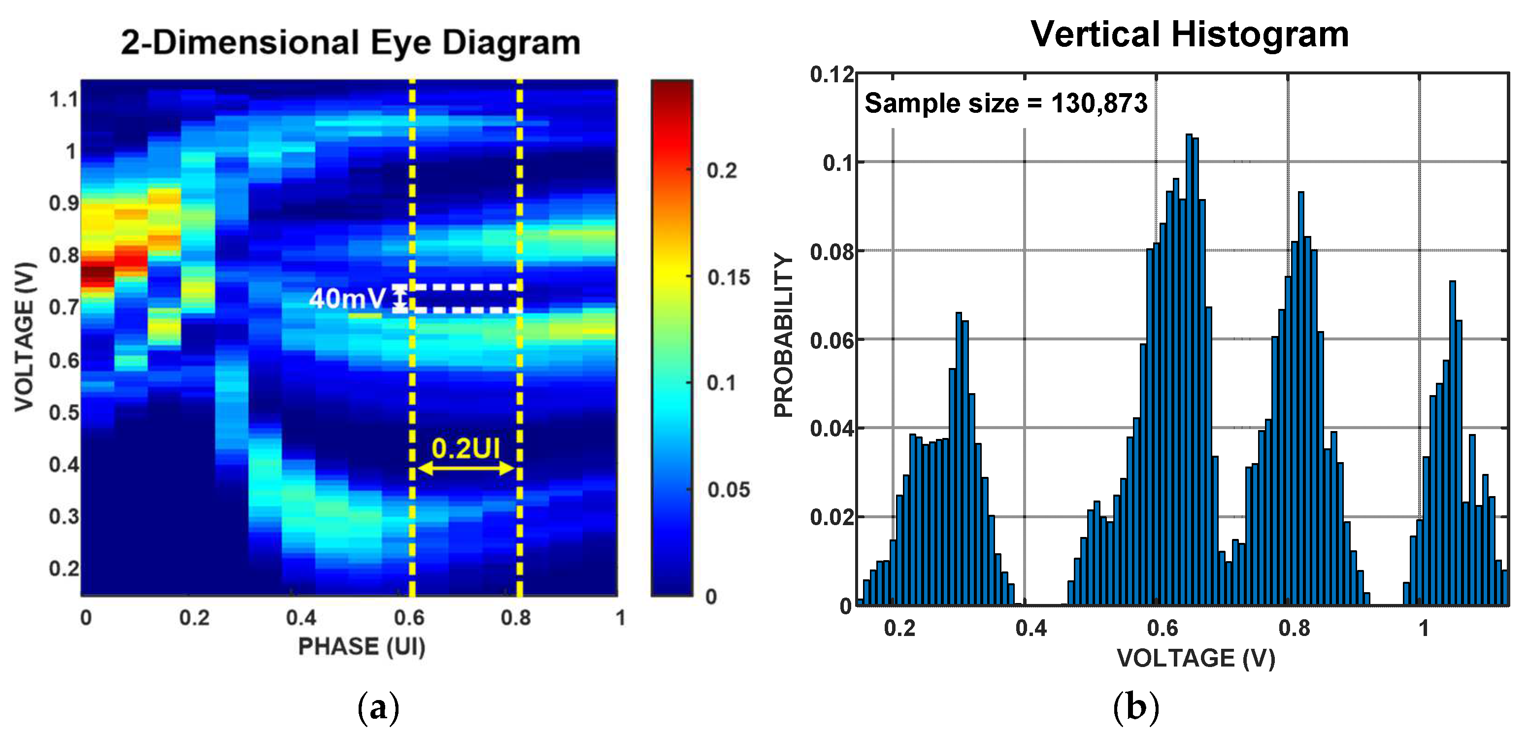
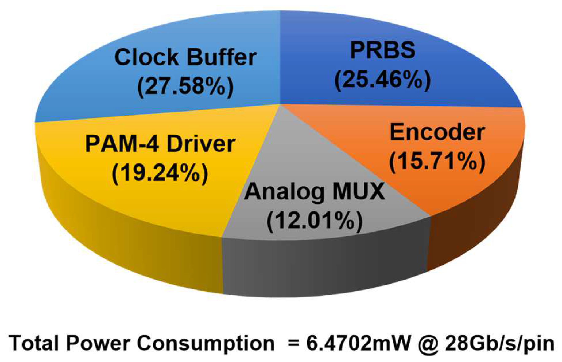
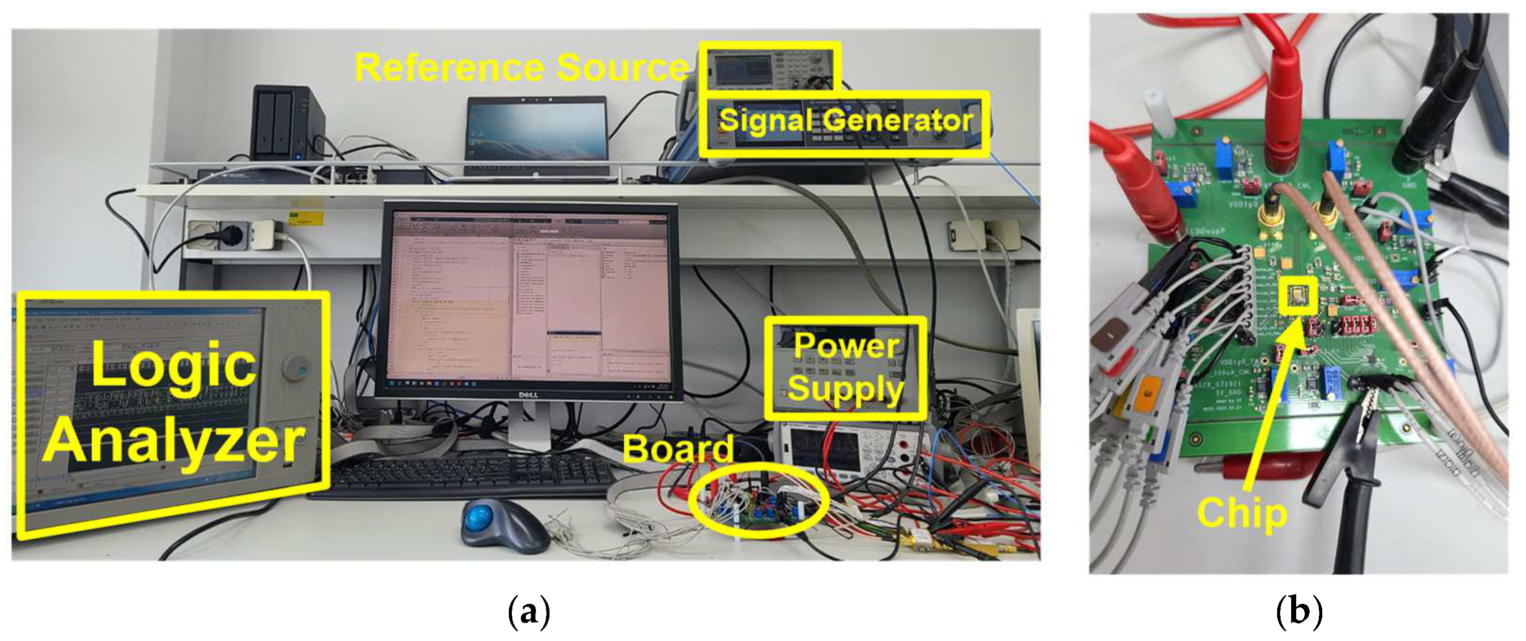
4. Measurement Results

Figure 6 shows the measurement setup and the test board for the prototype chip fabricated by the 28 nm CMOS process. The proposed TX and eye-monitor occupy 8670 μ m 2 and 2620 μ m 2 , respectively. The external signal source provides 7 GHz differential clock to the transmitter chip. The transmitter output waveform is captured by the embedded on-chip eye monitor by sweeping DTC control bits and DC reference voltages using two on-chip comparators. From the obtained outputs of the two comparators, we determine whether the voltage output of the channel lies between the two provided references at a specific time, which allows us to calculate the histogram of the voltage distribution and consequentially construct an eye diagram.
Figure 7 shows the obtained 28 Gb/s eye diagram by applying the described method as well as the vertical histogram of the signal at the end of the channel. Although our eye-measurement is limited by the timing resolution of the DTC as well as the accuracy of the externally provided references, the eye diagram shows that the worst-case horizontal eye opening is approximately 0.2 UI and the vertical eye opening is approximately 40 mV. Figure 7b shows the vertical histogram of the transmitter at specific DTC setting, which clearly shows four distinct levels.
The measured power breakdown is shown in Figure 8. With the VDDQ of 1.1 V, the total power consumption of the chip is 6.47 mW and the transmitter excluding the PRBS generator consumes roughly 75% of the total power. Table 1 compares the performance of the prototype transmitter with recently published single-ended transmitters. The proposed transmission achieves both the best energy efficiency of 0.17 pJ/b and the highest data rate among all high-speed single-ended transmitters even though the length of the channel used in the measurement is relatively shorter.

5. Conclusions

We presented a high-speed single-ended PAM-4 TX for a short-reach channel. Implemented by 28 nm CMOS process, the prototype chip achieved a data rate of 28 Gb/s/pin for the 100 μ m on-chip unterminated channel with a state-of-the-art energy efficiency of 0.17 pJ/b when using 1.1 V supply voltage. A key to achieving a high energy efficiency is using the capacitor and leaker to generate mid-level outputs instead of voltage division. With demonstrated performance, we believe that the proposed structure can be a promising transmitter topology for next-generation massively parallel on-chip interconnect systems.

Author Contributions

S.P. and J.K. proposed the architecture. S.P. designed the circuit and performed all measurements. S.P. wrote the initial manuscript and J.K. supervised the manuscript. All authors have read and agreed to the published version of the manuscript.

Funding

This work was supported in part by Samsung Chip Interconnect Solutions and by Institute of Information & Communications Technology Planning & Evaluation (IITP) grant funded by the Korea government (MSIT) (No. 2022-0-01171, A Development of Intelligent PHY Interface for High-Speed PIM Data Transfer).

Acknowledgments

The authors thank IDEC, KAIST, for the CAD tool support.

Conflicts of Interest

The authors declare no conflict of interest.

References

  1. Hollis, T.M.; Schneider, R.; Brox, M.; Hein, T.; Spirkl, W.; Bach, M.; Balakrishnan, M.; Dietrich, S.; Funfrock, F.; Ivanov, M.; et al. An 8-Gb GDDR6X DRAM Achieving 22 Gb/s/pin With Single-Ended PAM-4 Signaling. IEEE J. Solid-State Circuits 2022, 57, 224–235. [Google Scholar] [CrossRef]
  2. Kim, J.; Kundu, S.; Balankutty, A.; Beach, M.; Kim, B.C.; Kim, S.; Liu, Y.; Murthy, S.K.; Wali, P.; Yu, K.; et al. A 224 Gb/s DAC-Based PAM-4 Transmitter with 8-Tap FFE in 10 nm CMOS. In Proceedings of the 2021 IEEE International Solid-State Circuits Conference (ISSCC), San Francisco, CA, USA, 13–22 February 2021; pp. 126–128. [Google Scholar] [CrossRef]
  3. Hyun, C.; Jeong, Y.-U.; Kim, S.; Chae, J.-H. An 18-Gb/s/pin Single-Ended PAM-4 Transmitter for Memory Interfaces with Adaptive Impedance Matching and Output Level Compensation. Electronics 2021, 10, 1768. [Google Scholar] [CrossRef]
  4. Seo, J.; Lee, S.; Lee, M.; Moon, C.; Kim, B. A 20-Gb/s/pin 0.0024-mm2 Single-Ended DECS TRX with CDR-less Self-Slicing/Auto-Deserialization to Improve Tolerance on Duty Cycle Error and RX Supply Noise for DCC/CDR-less Short-Reach Memory Interfaces. In Proceedings of the 2022 IEEE International Solid-State Circuits Conference (ISSCC), San Francisco, CA, USA, 20–26 February 2022; pp. 1–3. [Google Scholar] [CrossRef]
  5. Kossel, M.; Toifl, T.; Francese, P.A.; Brändli, M.; Menolfi, C.; Buchmann, P.; Kull, L.; Andersen, T.M.; Morf, T. An 8Gb/s 1.5 mW/Gb/s 8-tap 6b NRZ/PAM-4 Tomlinson-Harashima precoding transmitter for future memory-link applications in 22 nm CMOS. In Proceedings of the 2013 IEEE International Solid-State Circuits Conference Digest of Technical Papers, San Francisco, CA, USA, 17–21 February 2013; pp. 408–409. [Google Scholar] [CrossRef]
  6. Lee, J.; Lee, W.; Cho, S. A 2.5-Gb/s On-Chip Interconnect Transceiver with Crosstalk and ISI Equalizer in 130 nm CMOS. IEEE Trans. Circuits Syst. I Regul. Pap. 2012, 59, 124–136. [Google Scholar] [CrossRef]
  7. Kulkarni, V.V.; Lim, W.Y.; Zhao, B.; Yan, D.L.; Wang, Y.S.; Zhou, J.; Arasu, M.A. A 5.1 Gb/s 60.3 fJ/bit/mm PVT tolerant NoC transceiver. In Proceedings of the 2016 IEEE Asian Solid-State Circuits Conference (A-SSCC), Toyama, Japan, 7–9 November 2016; pp. 141–144. [Google Scholar] [CrossRef]
  8. Lee, S.; Yun, J.; Kim, S. A 78.8 fJ/b/mm 12.0 Gb/s/Wire Capacitively Driven On-Chip Link Over 5.6 mm with an FFE-Combined Ground-Forcing Biasing Technique for DRAM Global Bus Line in 65 nm CMOS. In Proceedings of the 2022 IEEE International Solid-State Circuits Conference (ISSCC), San Francisco, CA, USA, 20–26 February 2022; pp. 454–456. [Google Scholar] [CrossRef]
  9. Mensink, E.; Schinkel, D.; Klumperink, E.A.M.; van Tuijl, E.; Nauta, B. Power Efficient Gigabit Communication Over Capacitively Driven RC-Limited On-Chip Interconnects. IEEE J. Solid-State Circuits 2010, 45, 447–457. [Google Scholar] [CrossRef]
  10. Hsu, Y.-Y.; Kuo, P.-C.; Chuang, C.-L.; Chang, P.-H.; Shen, H.-H.; Chiang, C.-F. A 7 nm 0.46 pJ/bit 20 Gbps with BER 1E-25 Die-to-Die Link Using Minimum Intrinsic Auto Alignment and Noise-Immunity Encode. In Proceedings of the 2021 Symposium on VLSI Technology, Kyoto, Japan, 13–19 June 2021; pp. 1–2. [Google Scholar]
  11. Park, H.; Choi, Y.; Sim, J.; Choi, J.; Kwon, Y.; Song, J.; Kim, C. A 0.385-pJ/bit 10-Gb/s TIA-Terminated Di-Code Transceiver with Edge-Delayed Equalization, ECC, and Mismatch Calibration for HBM Interfaces. In Proceedings of the 2022 IEEE International Solid-State Circuits Conference (ISSCC), San Francisco, CA, USA, 20–26 February 2022; pp. 1–3. [Google Scholar] [CrossRef]
Figure 1. (a) Overall architecture of the proposed PAM-4 TX for a short-reach channel and an eye monitor; (b) PAM-4 encoder input–output table; and (c) the timing diagram of the TX and eye monitor.
Electronics 11 02525 g001
Figure 2. Circuit implementation of the proposed PAM-4 driver.
Electronics 11 02525 g002
Figure 3. Operation of the PAM-4 driver.
Electronics 11 02525 g003
Figure 4. Simplified circuit diagram of the PAM-4 driver and the simulated eye diagram.
Electronics 11 02525 g004
Figure 5. (a) Micrograph of the prototype and (b) channel cross-section.
Electronics 11 02525 g005
Figure 6. (a) Measurement setup and (b) the test board.
Electronics 11 02525 g006
Figure 7. (a) Measured eye diagram from the on-chip eye monitor and (b) vertical histogram at the sampling clock phase.
Electronics 11 02525 g007
Figure 8. The power breakdown of the PAM-4 transmitter at 28 Gb/s/pin.
Electronics 11 02525 g008
Table 1. Performance comparison with other recent transmitters.
Low Speed On-Chip TransmitterHigh Speed On-Chip Transmitter
[9] JSSC’10[6] TCAS-Ⅰ’12[7] ASSCC’16[10] VLSI’21[11] ISSCC’22[4] ISSCC’22This work
Technology90 nm
CMOS
130 nm
CMOS
28 nm
CMOS
7 nm
CMOS
28 nm
CMOS
28 nm
CMOS
28 nm
CMOS
SignalingNRZNRZRZ/NRZNRZDi-codeNRZ (* DECS)PAM-4
Line TypeOn-chip
metal
On-chip
metal
On-chip
metal
Si-interposerOn-chip
Metal
On-chip
metal
On-chip
metal
Supply
Voltage(V)
1.2N/A0.9/10.81.0 (TX)/1.2 (RX)N/A1.1
Data Rate
(Gb/s)
22.54.420102028
Energy
Efficiency
** 0.28 pJ/b0.06 pJ/b0.0524 pJ/b/mm** 0.46 pJ/b** 0.385 pJ/b1.09 pJ/b0.17 pJ/b
Channel
Length
10 mm10 mm1 mm1 mm6 mm1 mm 100   μ m
Area (mm2)N/A0.00340.015N/A** 0.00460.0024280.008673
* Data embedded clock signaling ** Include RX.
Publisher’s Note: MDPI stays neutral with regard to jurisdictional claims in published maps and institutional affiliations.

