Article

A 48 GHz Fundamental Frequency PLL with Quadrature Clock Generation for 60 GHz Transceiver

1
National Mobile Communications Research Laboratory, School of Information Science and Engineering, Southeast University, Nanjing 210000, China
2
Purple Mountain Laboratory, Nanjing 210000, China
*
Authors to whom correspondence should be addressed.
Electronics 2022, 11(3), 415; https://doi.org/10.3390/electronics11030415
Submission received: 26 November 2021 / Revised: 27 January 2022 / Accepted: 27 January 2022 / Published: 29 January 2022
(This article belongs to the Special Issue Millimeter-Wave Integrated Circuits and Systems for 5G Applications)

Abstract

:
This paper presents a design of a 48 GHz CMOS phase-locked loop (PLL) for 60 GHz millimeter-wave (mmWave) communication systems. For the sliding intermediate frequency (sliding-IF) transceiver applications, a fundamental frequency PLL with quadrature clock generation scheme is proposed. Specifically, with an implicit capacitive-bridged shunt peaking network, a second order harmonic filtering technique is realized in the voltage control oscillator (VCO) to broaden the bandpass response, thereby avoiding the complex common-mode resonant tank calibration and improving the phase noise performance. A robust current mode logic (CML) static frequency divider topology is adopted to realize the prescaler and to generate the quadrature clock. With the capacitive-bridged shunt peaking load and robust biasing circuit, the static frequency divider locking range and high frequency performance is improved and its reliability is enhanced over the PVT corners. To improve the image suppression ratio of the transceiver, a quadrature clock phase calibration scheme is proposed and verified. Fabricated in a 65 nm CMOS process, the PLL occupies a core area of 800 μm × 950 μm. Over the frequency range of 45.2 to 52.6 GHz, the measured PLL in-band phase noise PLL is better than −90 dBc/Hz@100 KHz offset, and its jitter is less than 155 fs. Moreover, the reference spur is less than −60 dBc/Hz.

1. Introduction

With the wide bandwidth nature, the unlicensed 60 GHz band is considered as a solution for the several short distance and high data rate applications, such as wireless backhaul, augmented reality (AR), and virtual reality (VR). Benefiting from the aggressive scaling down of a CMOS transistor, several 60 GHz transceivers for wireless communication and radar sensing have been realized [1,2,3,4,5]. For above applications, the higher order modulation scheme, e.g., 16QAM, is required to achieve the high throughput rate. From the implementation perspective, due to very high operating frequency, the challenges are still imposed on the high-frequency transceiver building blocks. Particularly, as a key building block of the 60 GHz transceiver, the PLL is required with stringent phase noise, spur, and tuning range specifications.
In the past few years, several PLLs for mmWave applications have been reported. In [6], a 60 GHz chipset with 22.5–26.23 GHz integrated PLL, which achieved a phase noise of −92 dBc/Hz at 1 MHz offset, was realized with 0.13 μm BiCMOS process. In [7,8], all-digital mmWave PLL (ADPLL) was realized, but its in-band phase noise performance was limited to around −85 dBc/Hz. To improve the phase noise performance and attenuate the parasitic effect on the circuit operating frequency, frequency multiplication techniques, such as the injection locked oscillator [9,10], harmonic extraction [11], or push-push operation [12], were used. In [9], the injection locked oscillator was locked to 10th and 11th harmonics of the reference, obtaining the 20 GHz and 22 GHz quadrature clock with 132 mW power consumption. In [10], based on 20 GHz PLL and a 60 GHz sub-harmonic quadrature injection locked oscillator, a 60 GHz frequency synthesizer was realized in a 65 nm CMOS, achieving a phase noise of −96 and −117 dBc/Hz at 1 MHz and 10 MHz offset, respectively, at the cost of a large power consumption of the calibration loop. In [11], a 52 GHz frequency synthesizer was realized with VCO-doubler co-design, extracting the inherent 2nd harmonics of the differential oscillator. To realize differential output signal, the common gate and common source amplifiers were needed. It should be noticed that frequency multiplication techniques are typically sensitive to PVT issues and relative complex calibration schemes are needed. In [13], a 40 GHz mmWave sub-sampling PLL was realized with a 65 nm CMOS process, showing the advantages of low power consumption and low in-band phase noise performance. However, due to the narrow capture range of the sub-sampling, the sub-sampling PLL was sensitive to external disturbance and needed an extra control loop [14]. As an alternative approach, the reference sampling PLL offers a low in-band phase noise and a low spur performance. In [15], based on the reference sampling and injection-locked VCO (ILO) topology, a two stage 35 GHz mmWave frequency synthesizer was realized with a 45 nm CMOS process, achieving 251 fs rms jitter. To improve the working reliability, a digital frequency tracking loop was proposed. Also with the reference sampling topology, [16] proposed a reference oversampling digital PLL at low frequency. With the reference oversampling, the noise contribution from the loop components were suppressed, improving the in-band phase noise and making it possible to realize wide bandwidth and better oscillator noise filtering. Fabricated in a 28 nm CMOS, this PLL achieved 67.1 fs rms jitter at 4 GHz.
As two essential circuits, the VCO and high-speed frequency divider played important roles in determining the PLL phase noise and tuning range performance. To minimize the flicker noise up-conversion and improve the phase noise performance, the second harmonic filtering technique was introduced in a 1 GHz VCO [17]. An additional LC filter was needed, increasing the chip area occupation. In [18], the dual-core and multi-core LC tank schemes were proposed in a 35 GHz VCO, with the penalty of relatively large area and power consumption. Recently, the implicit common-mode resonance VCO topology was proposed without using any additional inductor. By introducing a common-mode resonance with common return path inductor, [19] proposed a 3 GHz VCO with an implicit common-mode resonance. With the common-mode resonance, high common-mode impedance was realized, increasing the VCO phase noise performance. A tunable common-mode capacitor array was intentionally employed in the VCO to achieve common-mode resonance at the second order harmonic frequency, with the penalty of increased VCO calibration complexity. In [20], together with explicit common-mode return path and embedded decoupled capacitor, the implicit second harmonic resonance was realized in a 30 GHz VCO, minimizing the flicker noise up-conversion and improving the phase noise performance. Moreover, the common-mode and differential-mode tank had a good frequency tracking with each other, improving the phase noise over the tuning range. To achieve high operating frequency, the injection-locked frequency dividers (ILFDs) can be used for mmWave PLL, but it is very sensitive to PVT corners [21,22]. In [23], as an alternative approach, to achieve fine frequency resolution, a 6.48 GHz delta-sigma fractional-N frequency divider was designed for 60 GHz transceiver with a 0.18-μm BiCMOS process. Note that to support high order quadrature amplitude modulation (QAM) modulation, the quadrature clock is needed, which has been realized with quadrature injection locked oscillator (QILO) [24] and poly-phase filters (PPF) [25]. For the QILO scheme, a complex calibration is required to ensure accurate phase performance and correct working, increasing the power consumption. For the PPF scheme, typically two or three stages are needed to achieve wideband PPF operation and accurate quadrature phase, therefore its insertion loss is relatively high.
To address above issues, targeting at the sliding-IF 60 GHz transceiver applications, a robust 48 GHz fundamental frequency PLL with 12 GHz quadrature clock generation scheme is proposed in this paper. Specifically, by introducing an implicit capacitive-bridged shunt peaking network, a broadband second order harmonic filter is realized in the VCO, thereby relaxing its common-mode resonant tank calibration issues and improving the phase noise performance. Moreover, with the benefits of the broadband capacitive-bridged shunt peaking load, a compact wide-locking range CML static divider is realized. To improve its reliability over the PVT corners, a feasible biasing scheme is employed. Different from QILO and PPF solutions, the 12 GHz quadrature clock is realized with the static CML frequency divider in this paper. To improve the image rejection ratio (IRR) performance, a phase calibration scheme is proposed and verified. Fabricated in a 65 nm CMOS process, the PLL achieves a measured in-band phase noise of better than −90 dBc/Hz @100 KHz offset from 45.2 to 52.6 GHz. Moreover, its jitter and reference spur are less than 155 fs and −60 dBc/Hz, respectively.
This paper is organized as follows. Section 2 briefly introduces proposed PLL topology for the 60 GHz sliding-IF transceiver. In Section 3, the design of the proposed mmWave VCO with a capacitive-bridged shunt peaking common-mode filtering technique is presented. Section 4 describes the implementation of a robust CML high speed frequency divider. Then, in Section 5, the quadrature clock phase calibration diagram is shown. In Section 6, the measurement results of the PLL are given. Finally, a summary is given in conclusion.

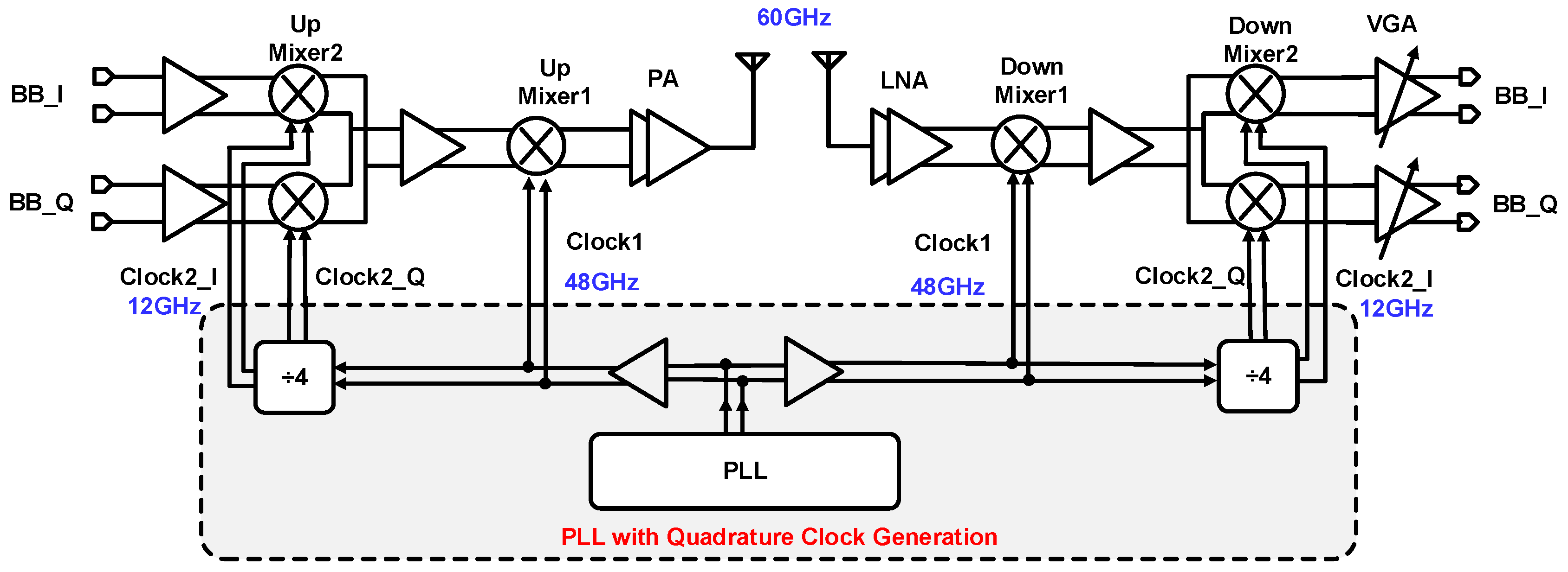
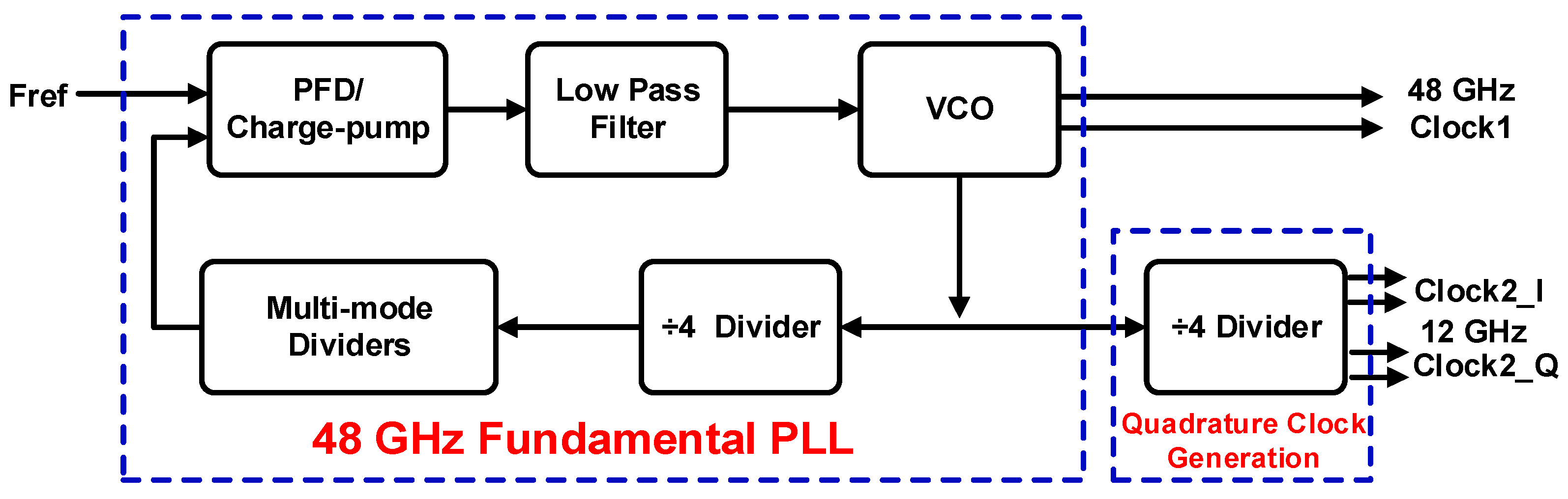
2. Proposed PLL Topology for the 60 GHz Sliding-IF Transceiver

Figure 1 shows a sliding-IF transceiver architecture [26,27]. To support the operation of the transceiver, a low phase noise integer-N fundamental frequency PLL topology is used, and the quadrature clock generation is also needed for the quadrature modulation/demodulation [27,28]. Compared with the direct conversion transceiver, the tuning range and operating frequency of the VCO and frequency dividers can be greatly reduced. Moreover, the pulling effect of the VCO due to strong interference from the power amplifier (PA) can be attenuated. As the operating frequency of the quadrature mixer is 12 GHz, it is also easier to calibrate quadrature clock to achieve better image injection performance.
Figure 2 shows the simplified block diagram of the PLL, in which the fundamental VCO is working at 48 GHz. By cascading two out-of-loop divide-by-2 frequency dividers, a divide-by-4 frequency divider is realized to generate the 12 GHz quadrature clock. Together with the programmable multi-modulus dividers (MMD), the in-loop divide-by-4 frequency divider divides the VCO output frequency further and compares with the 108 MHz reference clock through the phase/frequency detector (PFD). In the following sections, the design issues of the VCO and high-speed frequency divider will be discussed.

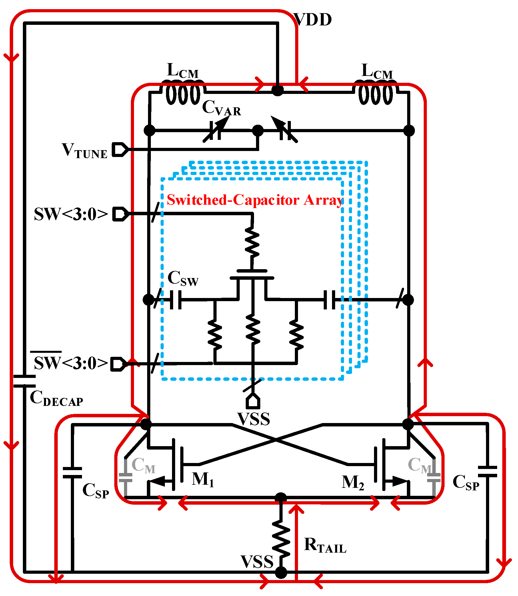
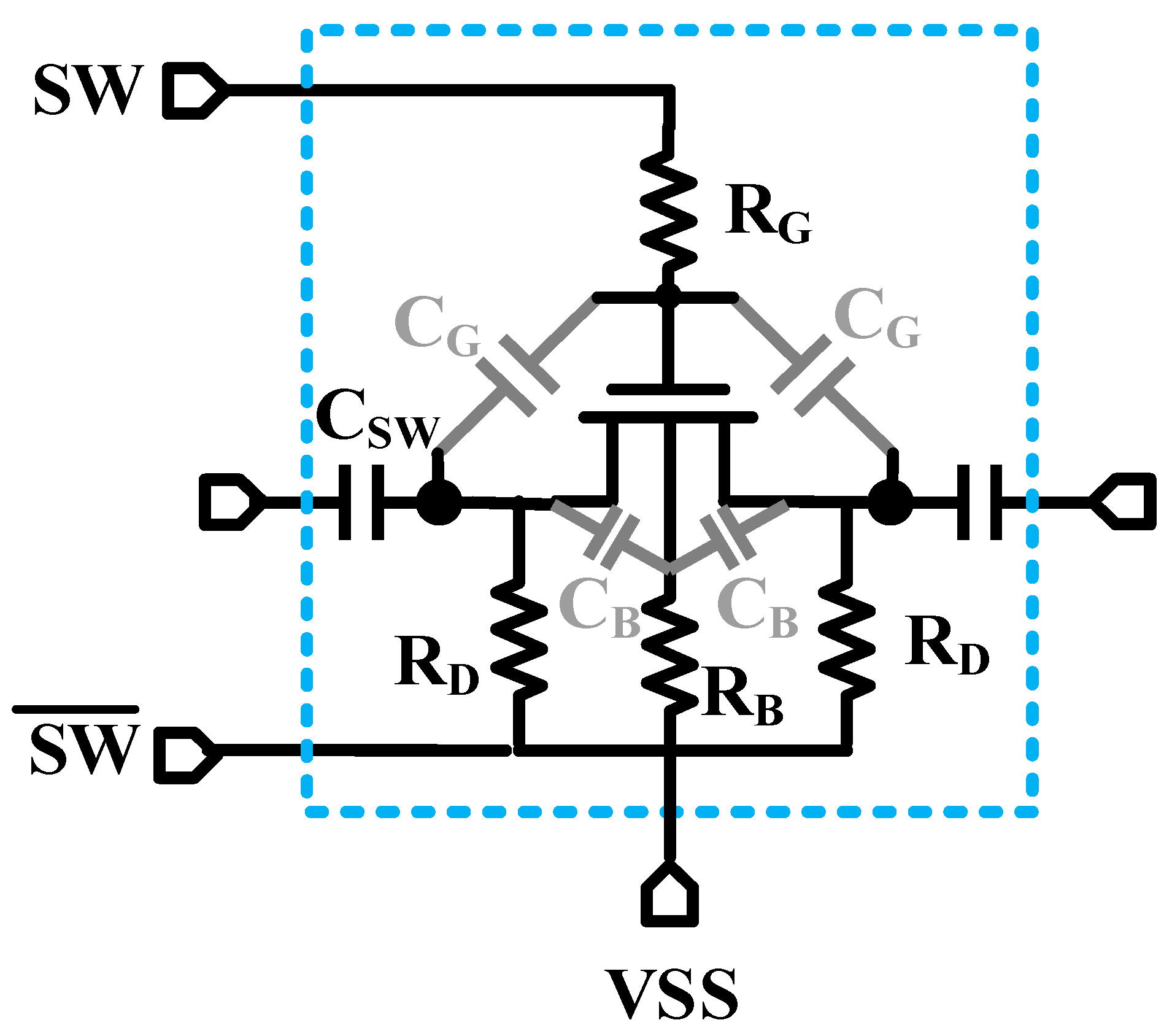
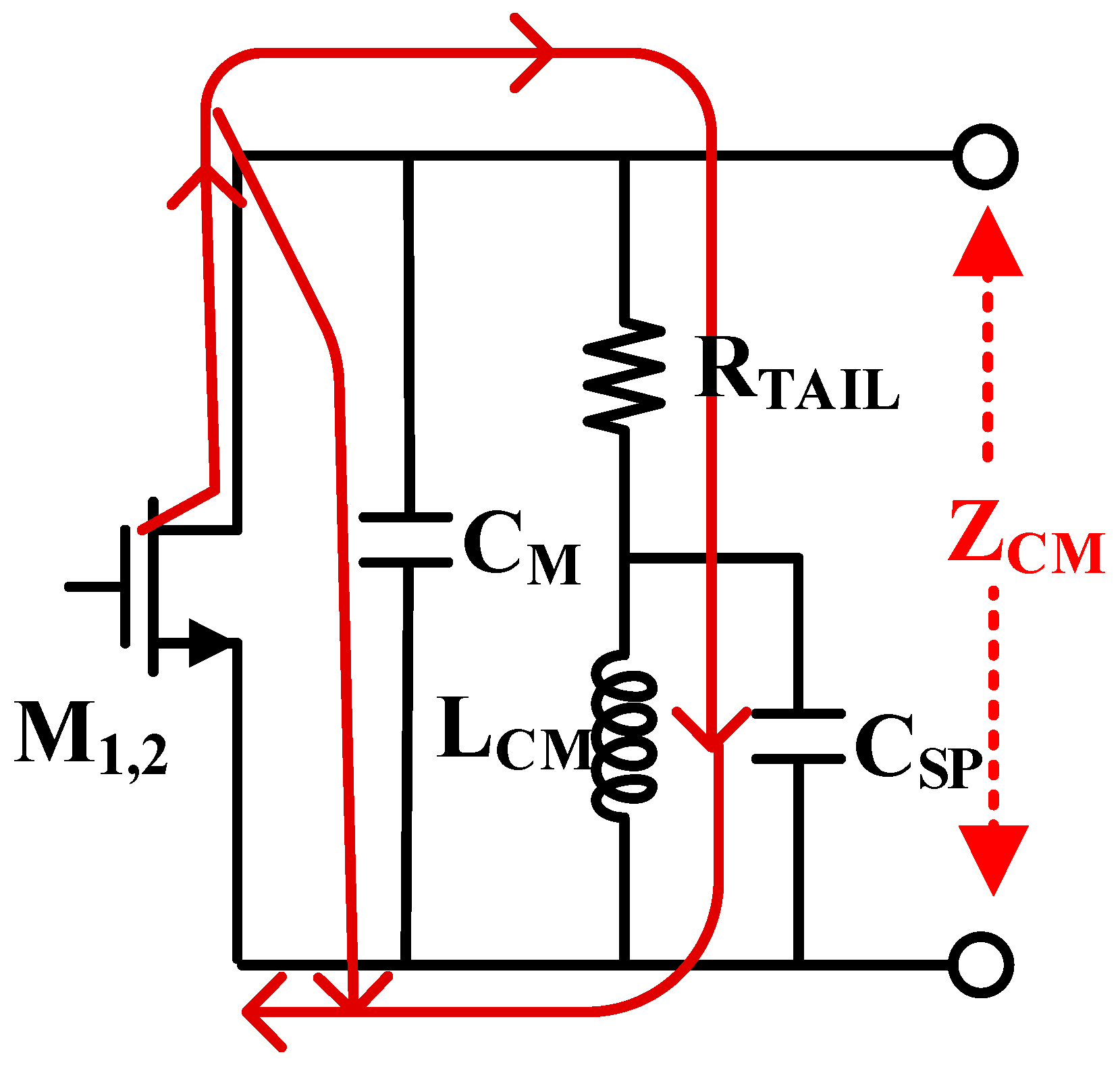
3. VCO Implementation

Figure 3 shows the implemented cross-coupled VCO topology. A 4-bit binary-weighted switched capacitor array is deployed to enhance the tank quality factor and to reduce KVCO, while a varactor is used to fulfill the frequency gaps between the 16 discrete frequency tuning curves. The differential resonant tank consists of the NMOS cross-coupled pair M1,2, the differential inductor LDM, switch capacitor CSW, varactor CVAR, and shunt capacitor CSP. Accordingly, its differential resonant frequency is given by:
f osc = 1 2 π L DM ( C SW + C VAR + C SP )
In this design, to increase the VCO phase noise performance, an implicit common-mode capacitive-bridged shunt peaking filter is realized by introducing tail resistor RTAIL and shunt capacitor CSP. As will be discussed shortly, by taking the advantage of the broadband characteristics of the capacitive-bridged shunt peaking network, a broadband common-mode resonance network is realized.
To illustrate the working mechanism of the implicit common-mode capacitive-bridged shunt peaking filter, Figure 4 shows the common-mode loop of the VCO. As indicated, the common-mode second harmonics current loop is composed of transistor M1,2, the common-mode tank inductor LCM, the shunt capacitor CSP, tail resistor RTAIL, and the switched-capacitor parasitic.
As an important part of the common-mode loop, the switch capacitor parasitic capacitance has an important effect. To illustrate this, Figure 5 shows the realized switched capacitor structure and the parasitics are highlighted. In this design, the triple-well CMOS process is used, and the resistors RG, RD, and RB with high value are inserted to bias the switch. Note that RG helps to reduce the parasitic capacitance between the switch gate and the switch control lines, while RD is used to block the switch capacitors CSW. Moreover, RB is used to isolate the buck parasitic capacitor CB from the ground VSS. In this way, the parasitic capacitance of the switched capacitors array is minimized in the common-mode loop, irrespective of whether the switch state is on or off.
For calculation convenience, Figure 6 shows the simplified common-mode topology. Note that together with the transistor M1,2 parasitic capacitor CM, an implicit capacitive-bridged shunt peaking network [29] is realized.
Accordingly, the common mode impedance between the cross-coupled pair M1,2 drain and source terminals, ZCM, can be derived as
Z CM = R TAIL ( 1 + s L CM / R TAIL + s 2 L CM C SP ) s 3 R TAIL L CM C SP C M + s 2 L CM ( C M + C SP ) + s C M R TAIL + 1
With calculation, it is found that the common mode impedance ZCM has 3 poles and 2 zeros. By carefully choosing the RTAIL and CSP value, the common-mode impedance ZCM can be optimized. For illustration, Figure 7a shows the simulated fundamental differential mode impedance ZDM, and the second harmonic common-mode impedance ZCM. The dashed lines show the fundamental differential mode impedance ZDM across the tuning range from 45 to 52.5 GHz. In contrast, the solid line indicates common-mode impedance ZCM. As indicated, ZCM is larger than 70 Ohm over 90 to 105 GHz, which is the second harmonic frequency of the fundamental frequency. In other words, a broadband high impedance is realized over large frequency range, relaxing the calibration requirements of the common-mode loop over a wide tuning range. For performance comparison, Figure 7b shows the simulated phase noise of the VCO with and without the proposed implicit second harmonic filter. Clearly, due to broadband high impedance in the common mode loop, the flicker noise performance is improved.
In this design, the tail resistor is also optimized to set the overdrive voltage for the cross-coupled transistors to be around 0.65 V, which is a near-optimal biasing voltage for the transistor in terms of speed, gm efficiency, and noise performance [30]. By tuning the varactor control voltage Vtune from 0.5 to 1.5 V, Figure 8 shows the simulation results of the VCO output frequency tuning curve. As indicated, the simulated tuning range is from 45.2 to 52.6 GHz. Note that with the overlapping of 16 discrete tuning curves, a continuous frequency coverage over the tuning range can be guaranteed.
The simulated performance of the VCO is compared with several publication results as shown in Table 1. Compared with >10 GHz oscillators, the proposed work yields the smallest area occupation and achieves the best FOM of −186.4 dBc/Hz, which is a widely accepted figure of merit and is defined as follows:
F O M = L { Δ f } 20 l o g ( f O / Δ f ) + 10 l o g ( P D C / 1 m W )

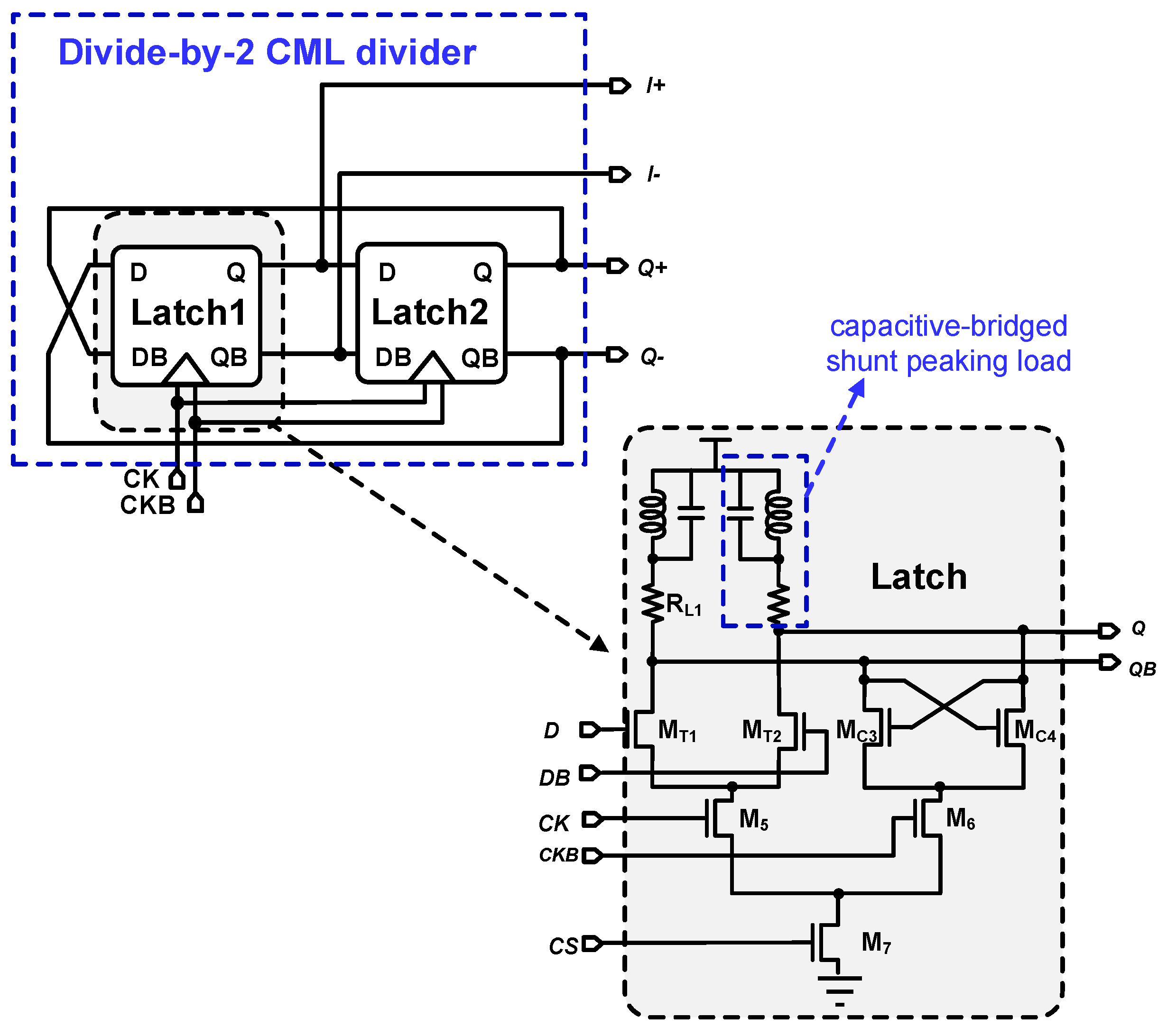
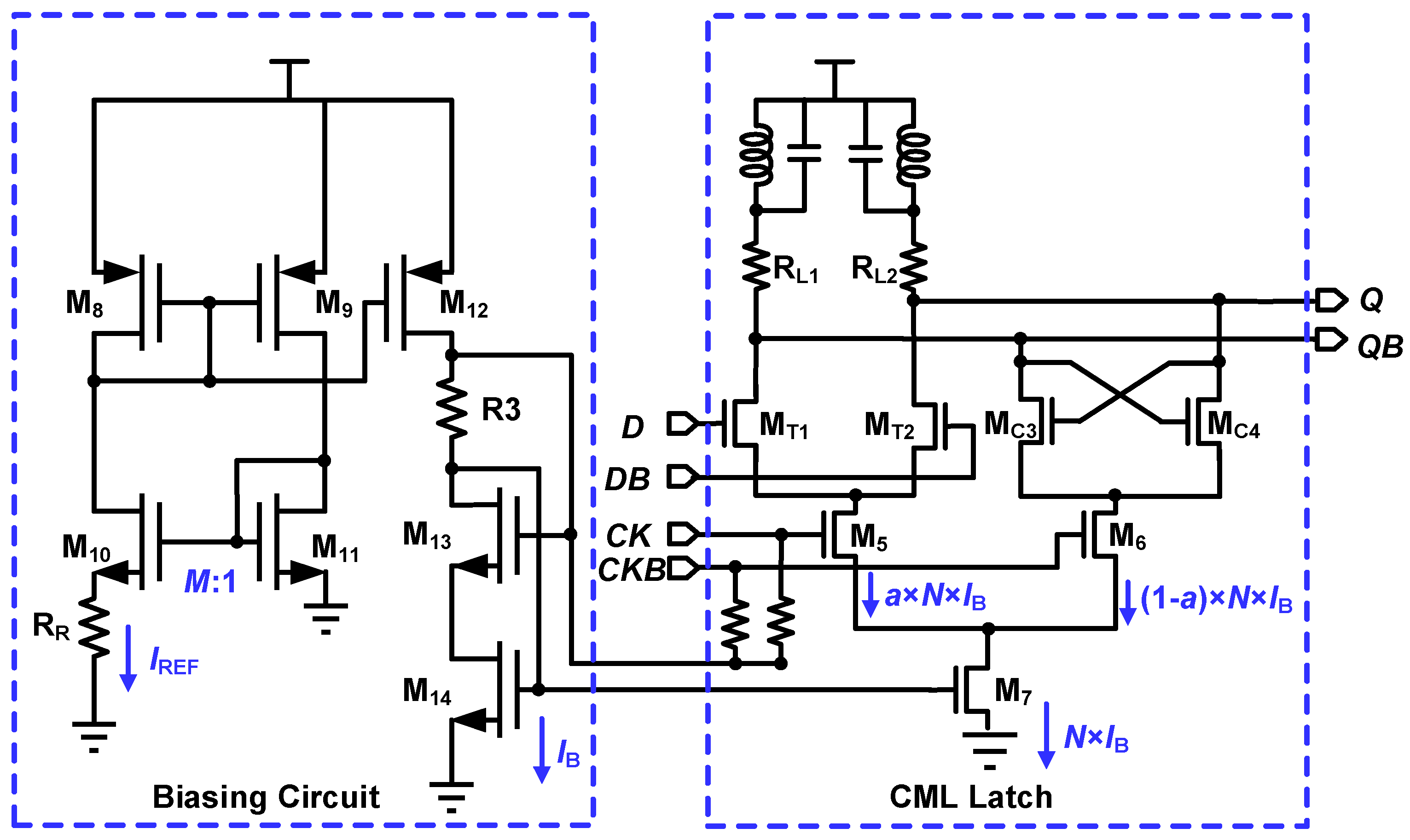
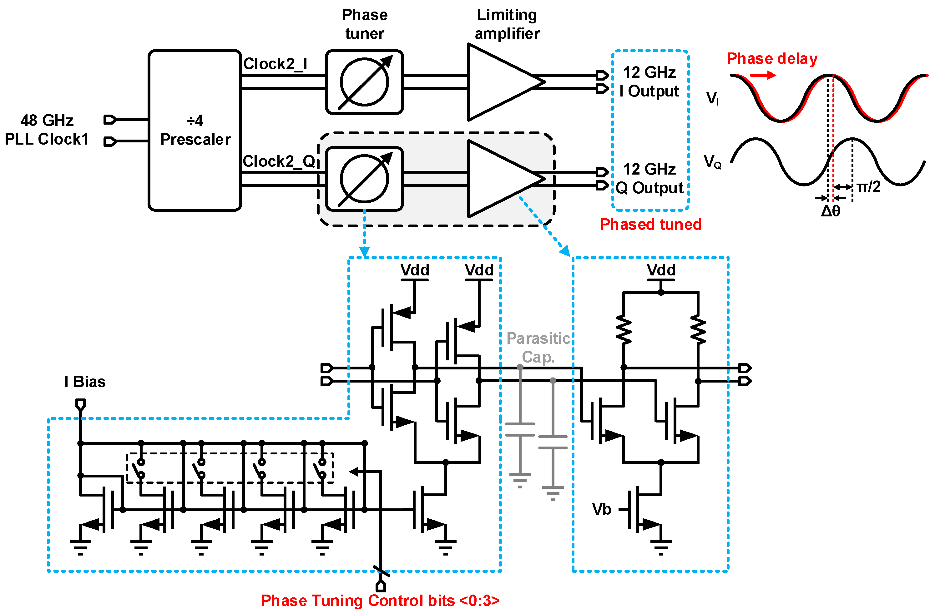
4. Frequency Dividers Implementation

As mentioned before, the frequency divider should operate at high frequencies with very large locking bandwidth in mmWave PLL. To address above mentioned PVT sensitivity issues of ILFD [21,22], it is highly desired to use static CML frequency divider in practice with its benefit of robustness over large locking range [31].
Based on the above consideration, the CML static frequency divider topology, as shown in Figure 9, is used in this design. As indicated, the divider consists of 2 D-latches with the capacitive-bridged shunt peaking load.
To improve the operating speed and bandwidth, the stack inductor is used as the load of the frequency divider. As shown in Figure 10, this stack inductor is realized with multiple coupled metal layers, and the space between the metal turns of the inductor is minimized. In this way, the inductor value is increased with magnetic coupling, reducing the inductor area substantially and introducing extra parasitic capacitor between the metal lines. By absorbing the parasitic capacitor in the inductor, a kind of capacitive-bridged shunt peaking network is realized. With simulations shown in the following sections, benefiting from the inductor and extra parasitic capacitor, the working speed and bandwidth of the frequency divider is improved substantially.
To optimize the divider performance and to ensure the robustness, the working mechanism of the D-latch flip-flop is discussed briefly as below. As indicated in Figure 9, the D-latch flip-flop consists of pre-amplifier transistors and cross-coupled transistors. When the input clock amplitude is zero, self-oscillation will be observed if the pre-amplifier and the cross-coupled pair have sufficient gain. Typically, to ensure correct operation of the divider with high power efficiency, it is better to set the self-oscillation frequency around the center of the input frequencies.
For calculation convenience, Figure 11 shows a simplified small signal model of the latch. In this small signal model, the cross-coupled pair produces a negative resistance, and it is controlled by its complementary output −VO.
Accordingly, the small signal gain AFD of the latch can be obtained as below
A FD = V 0 V i n = g m T R L 1 g m C R L
where gmT is the transconductance of the transistors MT1,T2, and gmC is the transconductance of the cross-coupled transistors MT3,T4. RL is the resistive load of the latch. Apparently, AFD is determined both by gmTRL and gmCRL product. To obtain a constant AFD value over different PVT corners, a constant gmR product biasing circuit is proposed, as shown in the left part of Figure 12. As will be discussed shortly, by using this biasing circuit, both gmTRL and gmCRL product can be kept constant over PVT corners.
The product of transconductance of M10 and resistor RR in the biasing circuit is expressed as
g m 10 R R = 2 × ( 1 ( W / L ) 11 ( W / L ) 10 )
Since M8, M9, and M12 have the same size, IB has the same value as IREF. In this design, the size ratio of transistor M14 and M7 is 1:N, so
I M 7 = N × I REF
Given the size ratio of M5 and M6 is a : ( 1 a ) , their currents are
I M 5 = a N × I REF
I M 6 = ( 1 a ) N × I REF
Consequently,
I MT 1 = I MT 2 = a 2 N × I REF
I MT 3 = I MT 4 = ( 1 a ) 2 N × I REF
In this design, the size ratio of M10 and MT1 is set to be 1 : a N , then
g m T 1 = 2 μ n C o x ( W / L ) 11 × I MT 1 = 2 μ n C o x a N ( W / L ) 10 × ( 1 2 a N × I REF ) = a N 2 g m 10
In the same way,
g m T 3 = ( 1 a ) N 2 g m 10
As a result,
g m T 1 R L = a N 2 R L R R g m 10 R R = 2 a N R L R R ( 1 ( W / L ) 11 ( W / L ) 10 )
g m T 3 R L = ( 1 a ) N 2 R L R R g m 10 R R = 2 ( 1 a ) N R L R R ( 1 ( W / L ) 11 ( W / L ) 10 )
As long as RL and RR are of the same type, according to Equations (4), (13) and (14), a very constant gain of the divider can be obtained over PVT corners by utilizing the proposed constant biasing circuit. To illustrate effect of the above biasing circuit, Figure 13 shows the simulated sensitivity curve of the 48 GHz divider-by-2 frequency divider under three temperature and process conditions. As indicated, the sensitivity curves are close to each other, and the locking range of the divider fully covers the VCO tuning range with 0 dBm input power under these three PVT cases.
The simulated performance of the proposed frequency divider is summarized in Table 2 and compared with several published mmWave frequency dividers. As indicated, the proposed design has the widest locking range among the publication results with a compact layout size. Note that the wide locking range is acquired without extra complex sub-bands tuning.

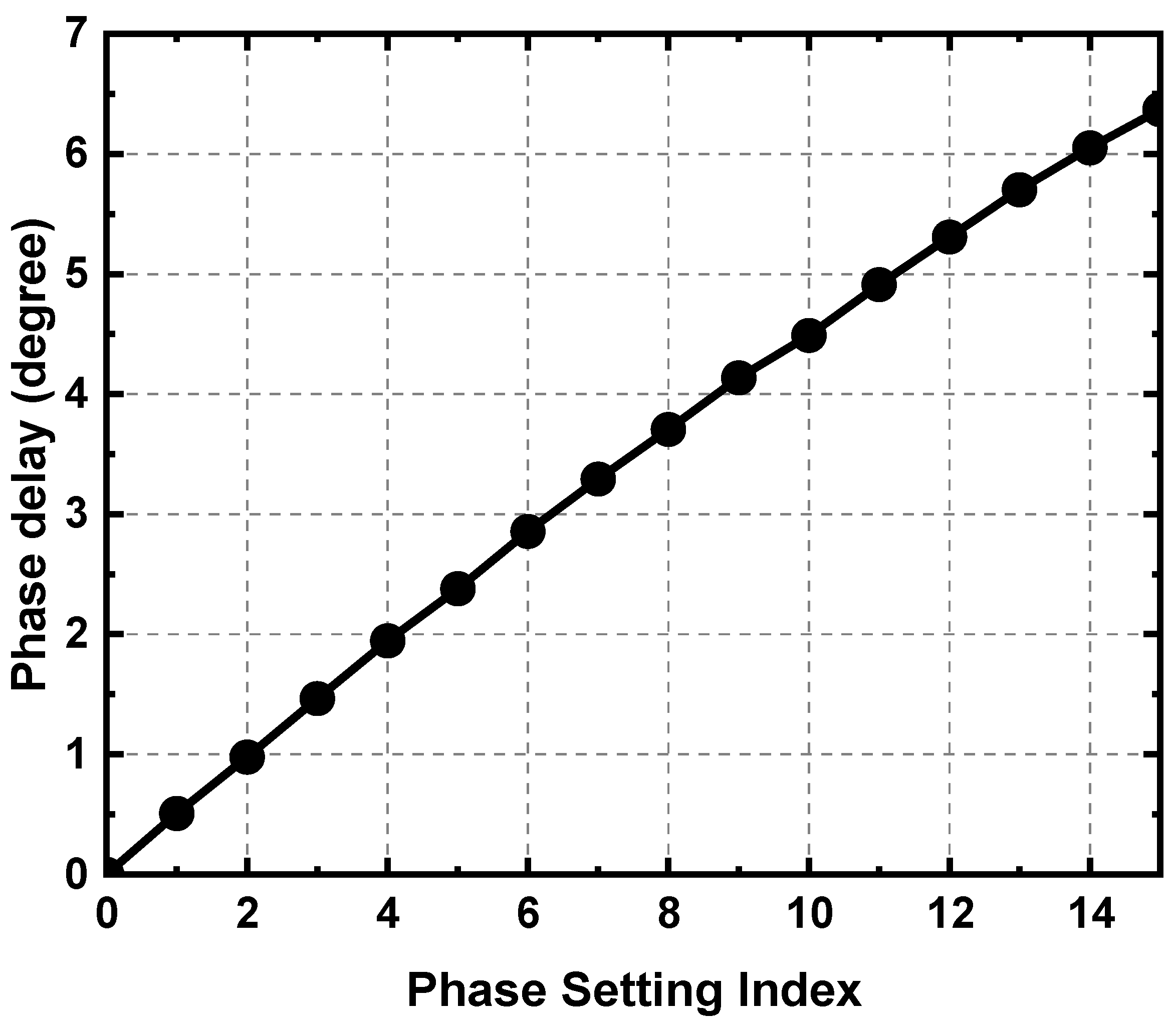
5. Quadrature Clock Calibration

For 60 GHz millimeter wave communication, the in-phase and quadrature (I/Q) signal imbalance performance is very critical. In general, the I/Q signal imbalance is measured by the IRR, which is defined as below
I R R = α 2 + 2 α cos Δ θ + 1 α 2 2 α cos Δ θ + 1
where α is the signal amplitude error, and it is defined as the ratio of I and Q signal output amplitude, θ the signal phase error. For the ideal matching, IRR tends to be ideal. However, there are some mismatches in reality within the quadrature mixer, worsening the IRR performance. Improving the IRR performance calls for the quadrature clock phase calibration.
As mentioned in Section 2, the 12 GHz 4-phases quadrature clock is generated with the out-of-loop divide-by-4 CML frequency divider. As shown in Figure 14, the quadrature clock phase error calibration is realized by tuning the phase delay of two 12 GHz output clocks. As indicated, it consists of the phase tuners and limiting amplifiers. The biasing current of the phase tuner is adjusted to change the charging and discharging speed of its output load capacitor, thereby changing the phase of the output signal with 4-bit digital control bits. With the above different phase setting states, the output amplitude of the phase tuner is constrained to be constant by the limiting amplifier, relaxing the conversion gain variation of the mixer.
Figure 15 shows the simulated phase delay with respect to the control bits. As indicated, the phase tuning range is about 6° with a 0.4° step, thereby making it possible to realize good IRR performance.

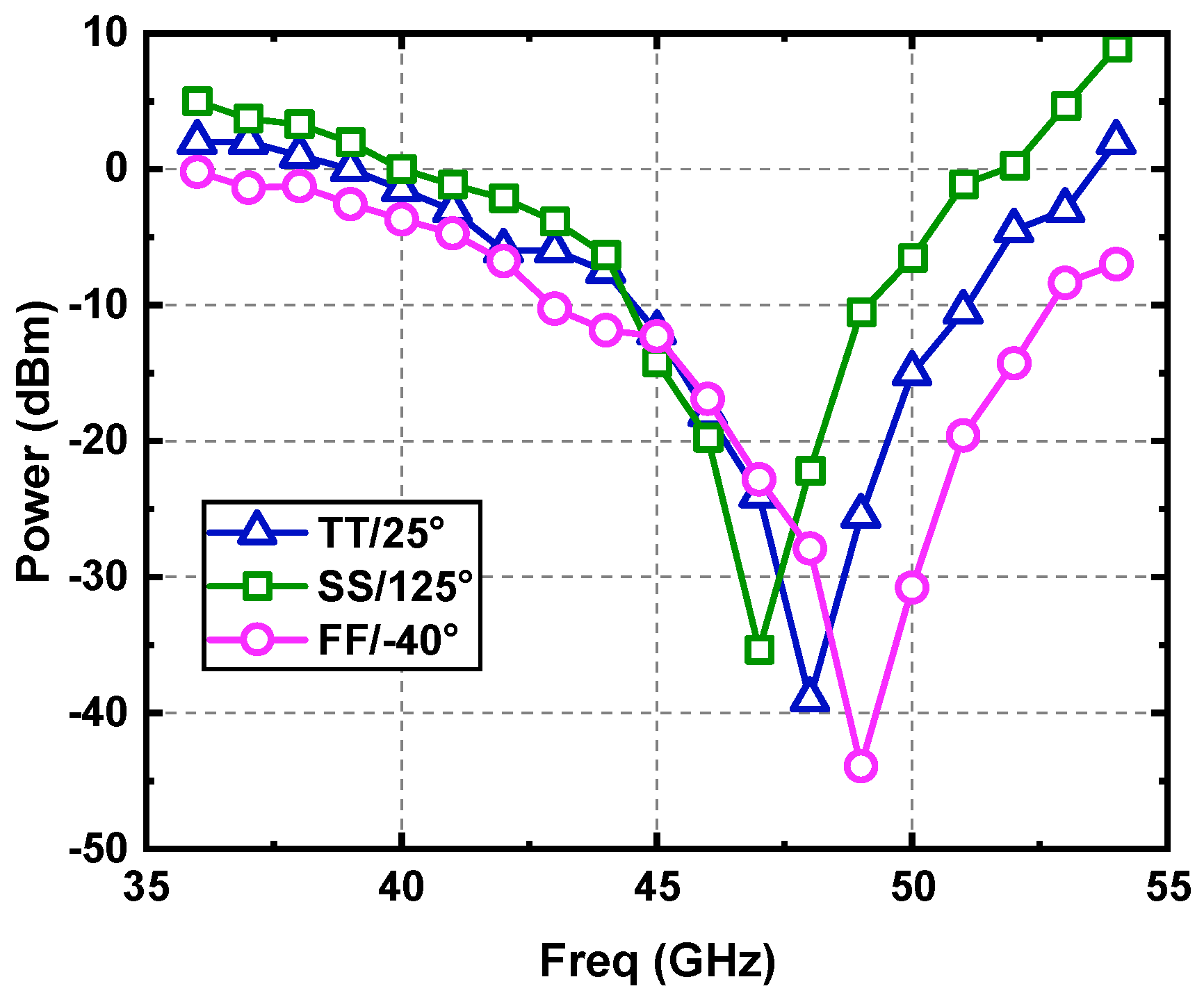
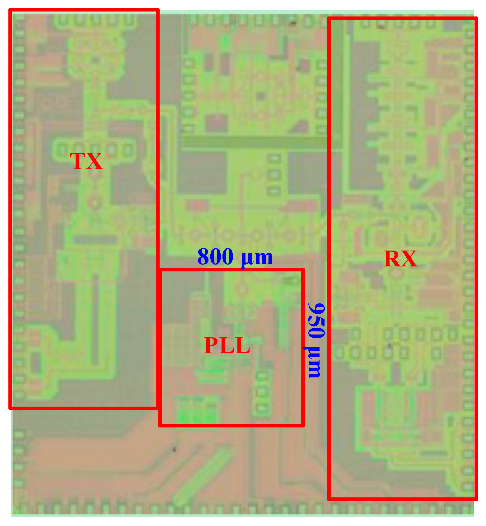
6. Measurement Results

Fabricated in a 65 nm CMOS process, Figure 16 shows the 60 GHz transceiver chip photograph. As indicated, the core chip area of the PLL is 800 μm × 950 μm, which integrated the 48 GHz PLL and quadrature clock generation circuits.
With a 108 MHz reference clock, by tuning division ratio of the MMD circuit, four typical clock frequencies (46.656, 48.384, 50.112, and 51.840 GHz) are generated, which correspond to four channel center frequencies of the 60 GHz band. Figure 17 shows the measured phase noise of these four frequencies. Clearly, benefiting from the above-mentioned design techniques of the VCO and frequency divider, the PLL can cover the four channels of the 60 GHz band, and the in-band phase noise is better than −90 dBc/Hz at 100 KHz offset. Figure 18 shows the measured reference spur at the above-mentioned four channel center frequencies. As indicated, the spurious performance of the PLL is less than −60 dBc.
Table 3 summarizes the measured PLL results at four channels of the 60 GHz bands. The power consumption of the PLL is about 80 mW. The integrated phase noise and RMS jitter are about −29 dBc and 155 fs, respectively.
Table 4 shows the performance comparison of this work with the state-of-the-art PLLs for the 60 GHz transceiver applications. As indicated, this fundamental PLL achieves the lowest jitter performance. Moreover, the in-band phase noise and spur performance are also very competitive.
With help of the receiver, the IRR performance can be measured. As mentioned before, by tuning the phase of the I- or Q-channel quadrature clock, an optimal IRR performance can be realized. As shown in Figure 19, IRR is better than 30 dB, which indicates that the phase difference of the quadrature signal after calibration is less than 3°.

7. Conclusions

Based on a 65 nm CMOS process, a fundamental frequency 48 GHz PLL with quadrature clock generation scheme was realized for the sliding-IF 60 GHz transceiver. With a capacitive-bridged shunt peaking network, an implicit broadband second harmonic filtering was realized, improving the VCO phase noise performance. Also with the capacitive-bridged shunt peaking network and robust biasing circuit, the working speed and locking range of the CML static frequency divider was improved, and its robustness was enhanced over PVT corners. A phase tuning scheme was presented for the quadrature clock calibration and was proven with IRR measurement results. With tests, this fundamental frequency PLL can cover four channel frequencies of the 60 GHz band and exhibited a phase noise and reference spur of lower than −92 dBc/Hz at 1 MHz offset and −60dBc, respectively. Moreover, its in-band phase noise was less than −90 dBc/Hz, and the integrated phase noise was less than −29 dBc, corresponding to a jitter less than 155 fs. With such results, the proposed PLL can be used for 60 GHz communication. Moreover, the proposed PLL was equally applicable to other mmWave bands, such as 5G NR 37–40 GHz and 64–71 GHz.

Author Contributions

Conceptualization, X.N., L.L., D.W. and X.W.; investigation, X.N., L.H., D.C. and L.L.; writing—original draft preparation, X.N., L.L. and X.W.; writing—review and editing, X.W. All authors have read and agreed to the published version of the manuscript.

Funding

This work was supported in part by the National Nature Science Foundation of China under Grant 61306030 and Grant 61674037, and in part by the Natural Science Foundation of Jiangsu Province of China under Grant BK20180368.

Conflicts of Interest

The authors declare no conflict of interest.

References

  1. Tabesh, M.; Chen, J.; Marcu, C.; Kong, L.; Kang, S.; Alon, E.; Niknejad, A. A 65 nm CMOS 4-element Sub-34mW/element 60 GHz phased-array transceiver. In Proceedings of the 2011 IEEE Solid-State Circuits Conference Digest of Technical Papers (ISSCC), San Francisco, CA, USA, 20–24 February 2011; pp. 166–168. [Google Scholar]
  2. Wu, R.; Minami, R.; Tsukui, Y.; Kawai, S.; Seo, Y.; Sato, S.; Kimura, K.; Kondo, S.; Ueno, T.; Fajri, N.; et al. 64-QAM 60-GHz CMOS Transceivers for IEEE 802.11ad/ay. IEEE J. Solid-State Circuits 2017, 52, 2871–2891. [Google Scholar] [CrossRef]
  3. Dasgupta, K.; Daneshgar, S.; Thakkar, C.; Kang, S.; Chakrabarti, A.; Yamada, S.; Narevsky, N.; Choudhury, D.; Jaussi, J.E.; Casper, B. A 60-GHz Transceiver and Baseband with Polarization MIMO in 28-nm CMOS. IEEE J. Solid-State Circuits 2018, 53, 3613–3627. [Google Scholar] [CrossRef]
  4. Lin, Y.; Chen, F.T.; Chen, W.Z. A Millimeter-Wave Frequency Synthesizer for 60 GHz Wireless Interconnect. In Proceedings of the 2020 International Symposium on VLSI Design, Automation and Test (VLSI-DAT), Hsinchu, Taiwan, 10–13 August 2020; pp. 1–2. [Google Scholar]
  5. Lee, W.; Dinc, T.; Valdes-Garcia, A. Multi-Mode 60-GHz Radar Transmitter SoC in 45-nm SOI CMOS. IEEE J. Solid-State Circuits 2020, 55, 1187–1198. [Google Scholar] [CrossRef]
  6. Ma, K.; Mou, S.; Mahalingam, N.; Wang, Y.; Thangarasu, B.K.; Yan, J.; Ye, W.; Wang, K.; Lim, W.M.; Wong, T.S.; et al. An Integrated 60GHz Low Power Two-Chip Wireless System Based on IEEE802.11ad Standard. In Proceedings of the 2014 IEEE MTT-S International Microwave Symposium (IMS2014), Tampa, FL, USA, 1–6 June 2014; pp. 1–6. [Google Scholar]
  7. Wu, W.; Staszewski, R.B.; Long, J.R. A 56.4-to-63.4 GHz Multi-Rate All-Digital Fractional-N PLL for FMCW Radar Applications in 65 nm CMOS. IEEE J. Solid-State Circuits 2014, 49, 1081–1096. [Google Scholar] [CrossRef]
  8. Hussein, A.; Vasadi, S.; Soliman, M.; Paramesh, J. 19.3 A 50-to-66GHz 65nm CMOS all-digital fractional-N PLL with 220fsrms jitter. In Proceedings of the IEEE International Solid-State Circuits Conference Digest of Technical Papers, San Francisco, CA, USA, 5–9 February 2017; pp. 326–327. [Google Scholar]
  9. Elbadry, M.; Sadhu, B.; Qiu, J.X.; Harjani, R. Dual-channel injection-locked quadrature LO generation for a 4-GHz instantaneous bandwidth receiver at 21-GHz center frequency. IEEE Trans. Microw. Theory Techn. 2013, 61, 1186–1199. [Google Scholar] [CrossRef]
  10. Deng, W.; Siriburanon, T.; Musa, A.; Okada, K.; Matsuzawa, A. A Sub-Harmonic Injection-Locked Quadrature Frequency Synthesizer With Frequency Calibration Scheme for Millimeter-Wave TDD Transceivers. IEEE J. Solid-State Circuits 2013, 48, 1710–1720. [Google Scholar] [CrossRef]
  11. Sadhu, B.; Ferriss, M.; Valdes-Garcia, A. A 52 GHz frequency synthesizer featuring a 2nd harmonic extraction technique that preserves VCO performance. IEEE J. Solid-State Circuits 2015, 50, 1214–1223. [Google Scholar] [CrossRef]
  12. Sadhu, B.; Kalia, S.; Harjani, R. A 3-band switched-inductor LC VCO and differential current re-use doubler achieving 0.7-to-11.6 GHz tuning range. In Proceedings of the IEEE Radio Frequency Integrated Circuits Symposium, Phoenix, AZ, USA, 17–19 May 2015; pp. 191–194. [Google Scholar]
  13. Wang, H.; Momeni, O. Low-Power and Low-Noise Millimeter-Wave SSPLL with Subsampling Lock Detector for Automatic Dividerless Frequency Acquisition. IEEE Trans. Microw. Theory Tech. 2021, 69, 469–481. [Google Scholar] [CrossRef]
  14. Lim, Y.; Kim, J.; Jo, Y.; Bang, J.; Yoo, S.; Park, H.; Yoon, H.; Choi, J. A 170MHz-Lock-In-Range and −253dB-FoMjitter 12-to-14.5GHz Subsampling PLL with a 150µW Frequency-Disturbance-Correcting Loop Using a Low-Power Unevenly Spaced Edge Generator. In Proceedings of the 2020 IEEE International Solid-State Circuits Conference (ISSCC), San Francisco, CA, USA, 16–20 February 2020; pp. 280–282. [Google Scholar]
  15. Liao, D.; Zhang, Y.; Dai, F.F.; Chen, Z.; Wang, Y. An mm-Wave Synthesizer With Robust Locking Reference-Sampling PLL and Wide-Range Injection-Locked VCO. IEEE J. Solid-State Circuits 2020, 55, 536–546. [Google Scholar] [CrossRef]
  16. Bertulessi, L.; Grimaldi, L.; Cherniak, D.; Samori, C.; Levantino, S. A low-phase-noise digital bang-bang PLL with fast lock over a wide lock range. In Proceedings of the 2018 IEEE International Solid—State Circuits Conference (ISSCC), San Francisco, CA, USA, 11–15 February 2018; pp. 252–254. [Google Scholar]
  17. Hegazi, E.; Sjoland, H.; Abidi, A. A filtering technique to lower LC oscillator phase noise. IEEE J. Solid-State Circuits 2001, 36, 1921–1930. [Google Scholar] [CrossRef] [Green Version]
  18. Fu, Y.; Li, L.; Wang, D.; Wang, X. A −193.6 dBc/Hz FoMT 28.6-to-36.2 GHz Dual-Core CMOS VCO for 5G Applications. IEEE Access 2020, 8, 62191–62196. [Google Scholar] [CrossRef]
  19. Fei, W.; Yu, H.; Yeo, K.S.; Lim, W.M. A 60GHz VCO with 25.8% Tuning Range by Switching Return-Path in 65nm CMOS. In Proceedings of the IEEE Asian Solid-State Circuits Conference 2012, Kobe, Japan, 12–14 November 2012; pp. 277–280. [Google Scholar]
  20. Hu, Y.; Siriburanon, T.; Staszewski, R.B. A Low-Flicker-Noise 30-GHz Class-F23 Oscillator in 28-nm CMOS Using Implicit Resonance and Explicit Common-Mode Return Path. IEEE J. Solid-State Circuits 2018, 53, 1977–1987. [Google Scholar] [CrossRef] [Green Version]
  21. Fu, H.; Fei, W.; Yu, H. A 60.8–67GHz and 6.3mW injection-locked frequency divider with switching-inductor loaded transformer in 65nm CMOS. In Proceedings of the 2014 IEEE MTT-S International Microwave Symposium (IMS2014), Tampa, FL, USA, 1–6 June 2014; pp. 1–4. [Google Scholar]
  22. Wong, Y.; Lin, W.; Tsai, J.; Huang, T. A 50-to-62GHz wide-locking-range CMOS injection-locked frequency divider with transformer feedback. In Proceedings of the 2008 IEEE Radio Frequency Integrated Circuits Symposium (RFIC), Atlanta, GA, USA, 15–17 June 2008; pp. 435–538. [Google Scholar]
  23. Wang, Y.; Ma, K.; Mahalingam, N.; Yeo, K.S. A delta-sigma fractional-N frequency divider for a Phase Lock Loop in 60GHz transceiver. In Proceedings of the 2011 IEEE International Conference of Electron Devices and Solid-State Circuits, Tianjin, China, 17–18 November 2011; pp. 1–2. [Google Scholar]
  24. Siriburanon, T.; Kondo, S.; Katsuragi, M.; Liu, H.; Kimura, K.; Deng, W.; Okada, K.; Matsuzawa, A. A Low-Power Low-Noise mm-Wave Subsampling PLL Using Dual-Step-Mixing ILFD and Tail-Coupling Quadrature Injection-Locked Oscillator for IEEE 802.11ad. IEEE J. Solid-State Circuits 2016, 51, 1246–1260. [Google Scholar] [CrossRef]
  25. Pang, J.; Wu, R.; Wang, Y.; Dome, M.; Kato, H.; Huang, H.; Narayanan, A.T.; Liu, H.; Liu, B.; Nakamura, T.; et al. A 28-GHz CMOS Phased-Array Transceiver Based on LO Phase-Shifting Architecture With Gain Invariant Phase Tuning for 5G New Radio. IEEE J. Solid-State Circuits 2019, 54, 1228–1242. [Google Scholar] [CrossRef]
  26. Mitomo, T.; Tsutsumi, Y.; Hoshino, H.; Hosoya, M.; Wang, T.; Tsubouchi, Y.; Tachibana, R.; Sai, A.; Kobayashi, Y.; Kurose, D.; et al. A 2-Gb/s throughput CMOS transceiver chipset with in-package antenna for 60-GHz short-range wireless communication. IEEE J. Solid-State Circuits 2012, 43, 3171–3460. [Google Scholar] [CrossRef]
  27. Sadhu, B.; Valdes-Garcia, A.; Plouchart, J.-O.; Ainspan, H.; Gupta, A.K.; Ferriss, M.; Yeck, M.; Sanduleanu, M.; Gu, X.; Baks, C.W.; et al. A 250-mW 60-GHz CMOS Transceiver SoC Integrated With a Four-Element AiP Providing Broad Angular Link Coverage. IEEE J. Solid-State Circuits 2020, 55, 1516–1529. [Google Scholar] [CrossRef]
  28. Li, L.; Niu, X.; Chen, L.; Yuan, C.; Tao, Z.; Jun, S.; Aili, W.; Ying, L.; Long, H.; Depeng, C.; et al. Design of 60 GHz RF Transceiver in CMOS: Challenges and Recent Advances. China Commun 2014, 11, 32–41. [Google Scholar]
  29. Shekhar, S.; Walling, J.S.; Allstot, D.J. Bandwidth Extension Techniques for CMOS Amplifiers. IEEE J. Solid-State Circuits 2006, 41, 2424–2439. [Google Scholar] [CrossRef]
  30. Fu, Y.; Li, L.; Wang, D.; Wang, X.; He, L. 28-GHz CMOS VCO With Capacitive Splitting and Transformer Feedback Techniques for 5G Communication. IEEE Trans. Very Large Scale Integr. (VLSI) Syst. 2019, 27, 2088–2095. [Google Scholar] [CrossRef]
  31. Katayama, K.; Amakawa, S.; Takano, K.; Fujishima, M. Parasitic conscious 54 GHz divide-by-4 injection-locked frequency divider. In Proceedings of the 2015 IEEE International Symposium on Radio-Frequency Integration Technology (RFIT), Senda, Japan, 26–28 August 2014; pp. 1–3. [Google Scholar]
  32. Chen, Z.; Wang, M.; Chen, J.; Liang, W.-F.; Yan, P.-P.; Zhai, J.F.; Hong, W. Linear CMOS LC -VCO Based on Triple-Coupled Inductors and Its Application to 40-GHz Phase-Locked Loop. IEEE Trans. Microw. Theory Tech 2017, 65, 2977–2989. [Google Scholar] [CrossRef]
  33. Yi, X.; Boon, C.C.; Liu, H.; Lin, J.F.; Lim, W.M. A 57.9-to-68.3 GHz 24.6 mW Frequency Synthesizer With In-Phase Injection-Coupled QVCO in 65 nm CMOS Technology. IEEE J. Solid-State Circuits 2014, 49, 347–359. [Google Scholar] [CrossRef]
  34. Abbas, W.; Mehmood, Z.; Seo, M. A V-Band Phase-Locked Loop with a Novel Phase-Frequency Detector in 65 nm CMOS. Electronics 2020, 9, 1502. [Google Scholar] [CrossRef]
Figure 1. Block diagram of the sliding-IF 60 GHz transceiver.
Electronics 11 00415 g001
Figure 2. The proposed PLL and quadrature clock generation circuit.
Electronics 11 00415 g002
Figure 3. Schematic of the implemented VCO.
Electronics 11 00415 g003
Figure 4. The common-mode loop of the VCO.
Electronics 11 00415 g004
Figure 5. The switched capacitor structures.
Electronics 11 00415 g005
Figure 6. The implicit capacitive-bridged shunt peaking filtering network.
Electronics 11 00415 g006
Figure 7. Simulated common-mode and differential-mode impedance and phase noise of the VCO: (a) The fundamental and second harmonic impedances over with the tuning range; (b) the simulated phase noise with and without the implicit second harmonic filter.
Electronics 11 00415 g007
Figure 8. Simulated frequency tuning curve of VCO.
Electronics 11 00415 g008
Figure 9. Proposed CML static frequency divider structure.
Electronics 11 00415 g009
Figure 10. Implementation of the stack inductor.
Electronics 11 00415 g010
Figure 11. The small-signal model of the D-latch.
Electronics 11 00415 g011
Figure 12. The proposed biasing circuit of the frequency divider.
Electronics 11 00415 g012
Figure 13. Simulated sensitivity curves of the frequency divider.
Electronics 11 00415 g013
Figure 14. Diagram of the phase tuning circuits.
Electronics 11 00415 g014
Figure 15. Phase delay with respect to the control bits.
Electronics 11 00415 g015
Figure 16. Photography of the 60 GHz CMOS transceiver with the integrated PLL.
Electronics 11 00415 g016
Figure 17. Measured phase noise of the PLL: (a) 46.656 GHz; (b) 48.384 GHz; (c) 50.112 GHz; (d) 51.840 GHz.
Electronics 11 00415 g017
Figure 18. Measured reference clock spurious of the PLL: (a) 46.656 GHz; (b) 48.384 GHz; (c) 50.112 GHz; (d) 51.840 GHz.
Electronics 11 00415 g018
Figure 19. The measured IRR performance of the receiver.
Electronics 11 00415 g019
Table 1. VCO performance summary and comparison.
References[19][20][18]This Work
65 nm28 nm65 nm65 nm
Oscillation Frequency (GHz)51.9–67.327.3–31.228.6–36.245.2–52.6
Tuning Range (GHz)16.41423.515.1
PN@1MHz (dBc/Hz)−80−106−103−99
Power consumption (mW)5.411.64.65
FOM−168−184−186.2−186.4
Core Aera (mm2)0.030.0640.120.018
Table 2. Frequency divider performance summary and comparison.
References[21][22][31]This Work
Technology65 nm130 nm65 nm65 nm
ArchitectureILFDILFDILFDCML
Operation Frequency (GHz)60.8–6749.8–62.053.9–54.238–54
Locking Range6.212.20.816
Power Consumption (mW)6.310.82114
Core Area (mm²)0.058<0.320.0050.008
Sub-bands Tuning NeededYesNoNoNo
Table 3. PLL measurement results at four channels of the 60 GHz band.
Channel 1Channel 2Channel 3Channel 4
Frequency (GHz)46.65648.38450.11251.84
Int.PN (dBc)−29.4−29−29.2−28.8
Int.PN (Degree)2.72.92.82.9
RMS Jitter (fs)163165155157
PN@1MHz (dBc/Hz)−93.7−93.8−92.8−92.3
Spur (dBc)−63−65−64−62
Power consumption (mW)75777880
Table 4. Performance comparison with the state-of-the-art PLL for 60 GHz applications.
References[7][8][15][24][32][33][34]This Work
TopologyADPLLADPLLSSPLLSSPLL
+ QILO
PLL +
Doubler
CP PLL
+ QVCO
CP PLLCP PLL
Technology65 nm65 nm GP45 nm65 nm90 nm65 nm65 nm
LP
65 nm
LP
Locking range (GHz)56.4–63
(11.6%)
50–66.5
(28%)
33.6–36
(6.9%)
55.6–65
(15.9%)
38.6–45
(14.3%)
57.9–68
(16.5%)
65–67.4
(1.6%)
45.2–52.56 (15%)
Fref (MHz)1001008036/4033.75135515108
In-band PN (dBc/Hz)−75−79–−83--−78.5−82.5−91–−84--<−90
PN@1MHz (dBc/Hz)−90−88–−93−94.992<−80−89.8−84.4<−92
RMS jitter (fs)590.2223–261251290--238--155–165
Spur (dBc)−74−59–−68<−60−73−46−54--<−60
Area (mm2)0.480.450.411.081.380.190.37<0.72
Power consumption (mW)484620.6327624.68880
Publisher’s Note: MDPI stays neutral with regard to jurisdictional claims in published maps and institutional affiliations.

