Article

A Wide-Band Divide-by-2 Injection-Locked Frequency Divider Based on Distributed Dual-Resonance Tank

School of Electronic Science and Engineering, University of Electronic Science and Technology of China, Chengdu 611731, China
*
Author to whom correspondence should be addressed.
Electronics 2022, 11(4), 506; https://doi.org/10.3390/electronics11040506
Submission received: 31 December 2021 / Revised: 27 January 2022 / Accepted: 31 January 2022 / Published: 9 February 2022
(This article belongs to the Special Issue Millimeter-Wave Integrated Circuits and Systems for 5G Applications)

Abstract

:
A wide-band divide-by-2 injection-locked frequency divider (ILFD) based on a distributed dual-resonance high-order tank is presented. The ILFD employs a distributed LC network as the dual resonance tank and achieves an ultra-wide locking range. Fabricated in a 65 nm 1P7M LP-CMOS process, the divide-by-2 ILFD consumes 7 mW from a 0.7 V power supply and realizes a locking range of 87.0%, from 13 GHz to 33 GHz. The core circuit occupies an area of 0.22 mm × 0.5 mm.

1. Introduction

In modern RF phase-locked loops, the frequency divider is one of the critical buildings. Among various dividers, the injection-locked frequency divider (ILFD) draws most of the attention, as it can work at a higher frequency and consume less power.
An original ILFD injects the input signal indirectly from the tail transistor of an oscillator [1]. However, this indirect injection topology entails two issues. Firstly, the injected current may flow to the ground through the parasitic capacitance at the common node and cause a loss of injected current. Secondly, the injected current is steered to the tank through two switch transistors, and the current gain from the injection current to the tank is 2/π, less than 1. Thus, the indirect injection topology is of low current injection efficiency. Reference [2] proposed a direct injection topology, where the input signal is directly injected into the tank. Though coming to a larger locking range as compared to its indirect injection counterpart, the direct injection ILFD is still limited to a relatively narrow locking range. In Reference [3], a multi-order LC oscillator is used to expand the locking range to 25.9%. In References [4,5], a wide-band ILFD was realized by a transformer-based fourth-order resonator. The work in [4] was further investigated in [6], and the locking range was expanded to 62.9%. In this case, however, a transformer with a low coupling factor was needed. The transformer should be carefully designed and occupy a large layout area due to the low coupling factor.
This paper proposes a wide-band divide-by-2 ILFD implemented in the 65 nm 1P7M LP-CMOS process. The ILFD uses a distributed dual-resonance resonator to expand the locking range. The analysis of the dual-resonance tank is presented in Section 2. Implementations and measurement results are shown in Section 3. Section 4 investigates the electromagnetic (EM) coupling of the inductors. Finally, the conclusion is given in the last section.

2. Analysis of the Proposed Dual-Resonance Tank

An ILFD functions as a free-running oscillator and has an oscillation frequency fosc, if no signal is injected in. When the injected signal is large enough, the ILFD will oscillate at a new frequency fnew determined by the injection signal. At the free-running frequency fosc, the phase response of the tank impedance is zero, while at the new frequency fnew, a phase shift is induced by the tank. The injected current should be able to compensate for this phase shift to sustain the ILFD oscillating at the new frequency fnew.
The total current Itank flowing into the tank consists of the oscillating current Iosc and the injection current Iinj, that is:
I tank = I osc + I inj
A phase shift occurs between the current Itank and the voltage Vtank at the tank, if the operating frequency deviates from the resonating frequency of the tank. In order to sustain the waveform in the oscillator, Iosc and Vtank should be in phase with each other. Refer to Figure 1a,b, the maximum θmax is obtained when Iinj is perpendicular to Iosc:
sin θ max = I inj / I osc
Thus, the phase shift caused by the tank should be less than θmax:
Z tank ( ω ) < arcsin ( I inj / I osc )
With a given Iinj and Iosc, a large locking range can be obtained if the phase shift caused by the tank is kept near zero across a large frequency range.

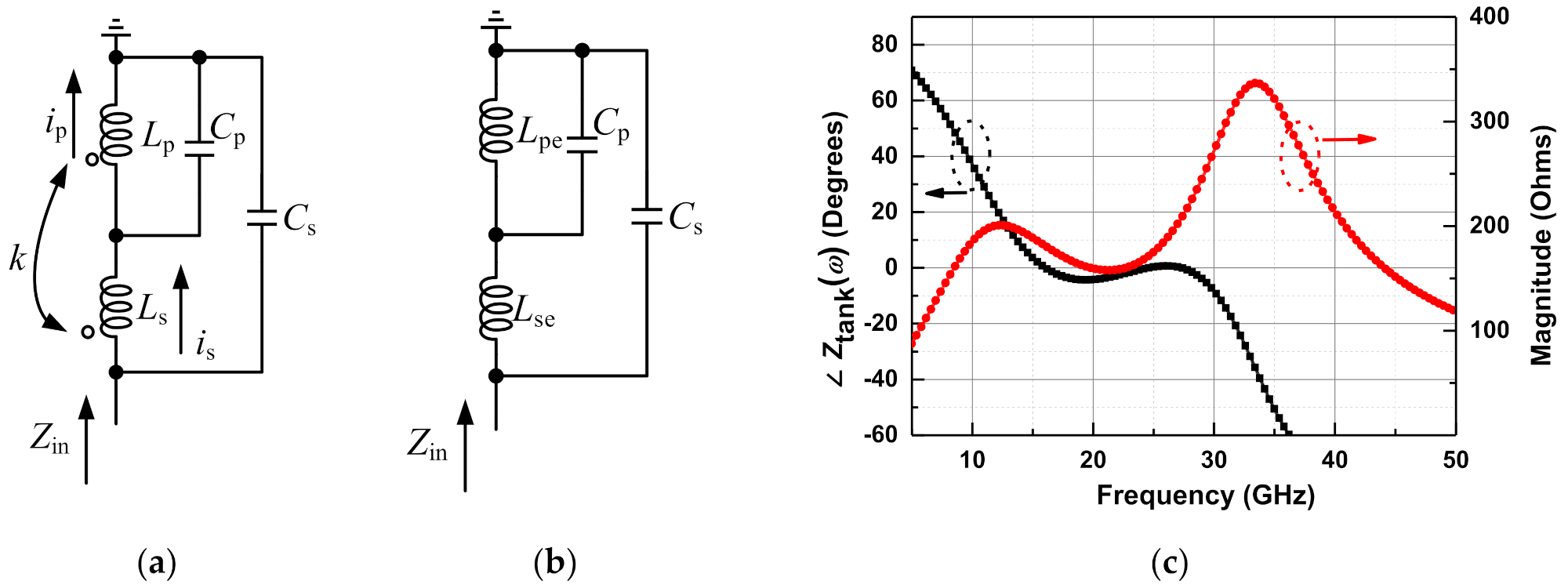
2.1. Zero and Pole Analysis
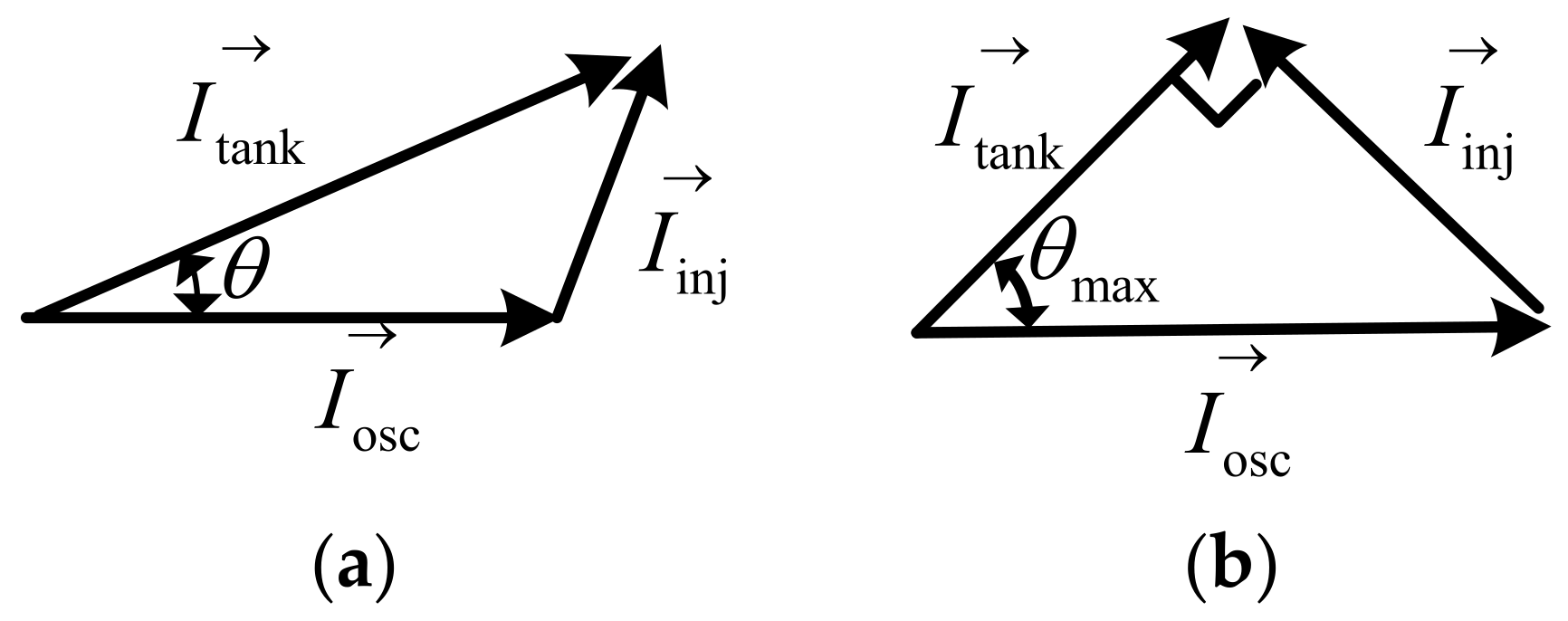
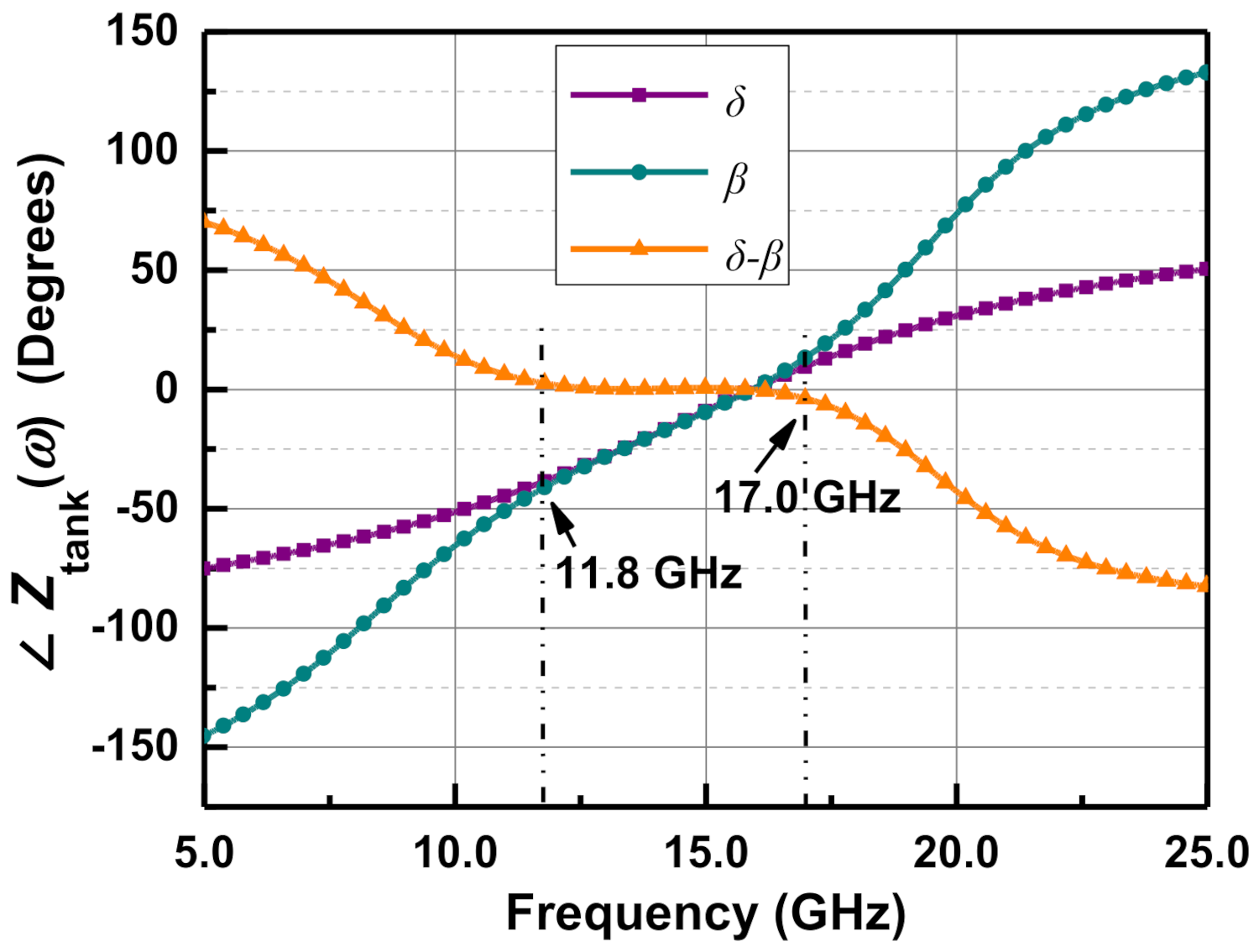
Figure 2a shows the conceptual diagram of the proposed divide-by-2 ILFD, and Figure 2b is a simplified AC equivalent circuit of the tank in the ILFD. The input impedance of the dual-resonance tank can be written as:
Z in ( s ) = 1 s C s ( s L s + ( s L p ) 1 s C p )
Replacing s with jω, we can obtain:
Z in ( j ω ) = j ω ( L p + L s ω 2 L p L s C p ) 1 ω 2 ( L p C p + L p C s + L s C s ) + ω 4 L p L s C p C s
From (5), the tank owns two pole frequencies and one zero frequency. Defined as:
ω 1 = 1 L p C p , ω 2 = 1 L s C s , b = ω 1 2 ω 2 2 ,   and   a = C s C p
Thus, the zero frequency ωz and the two pole frequencies ωp1 and ωp2 are given as:
ω z 2 = ( b + a ) ω 2 2
ω p 1 2 = ω 2 2 2 ( b + a + 1 + ( b + a + 1 ) 2 4 b )
ω p 2 2 = ω 2 2 2 ( b + a + 1 ( b + a + 1 ) 2 4 b )
If the zero frequency ωz is set to be equal to ω2, that is, b + a=1, then:
ω p 1 2 = ω 2 2 ( 1 a )
ω p 2 2 = ω 2 2 ( 1 + a )
The two pole frequencies ωp1 and ωp2 are located at the left side and right side of the zero frequency ωz, respectively. Thus, following the method proposed in [4], if the losses of the inductor and capacitor are considered, the phase variety caused by the zero frequency may be compensated by the two pole frequencies. This compensation may result in a zero-phase-shift (ZPS) plateau in the phase response of the tank around the zero frequency ωz, and lead to a larger locking range.

2.2. Phase Response

Taking the loss of the inductor Lp into consideration, the tank impedance in (4) may be re-written as:
Z in ( s ) = 1 s C s ( s L s + ( s L s ) 1 s C p | | R p )
Z in ( j ω ) = L p L s ω 2 + j ω R p ( L p + L s L p L s C p ω 2 ) R p [ 1 ω 2 ( L p C p + L p C s + L s C s ) + ω 4 L p L s C p C s ] + j ω L p ( 1 L s C s ω 2 ) = A e j δ B e j β
wherein A and B are real values greater than 0, and:
tan ( δ ) = ω R p ( L p + L s ω 2 L p L s C p ) L p L s ω 2 = R p C p ω 2 ω z 2 ω
tan ( β ) = ω L p ( 1 L s C s ω 2 ) R p [ 1 ω 2 ( L p C p + L p C s + L s C s ) + ω 4 L p L s C p C s ]
tan ( β ) = ω R p C p ω 2 ω 2 2 ( ω 2 ω p 1 2 ) ( ω 2 ω p 2 2 )
The phase shifts δ and β exhibit the same sign when ω is located between ωp1 and ωp2. The slopes of the two phase shifts versus frequency are determined by RpCp, and the two slopes show opposite dependences on RpCp. If RpCp is properly selected, the two phase shifts may cancel each other out across a wide bandwidth. Based on the tank shown in Figure 3a, Figure 4 presents the calculated δ and β from (14) and (15), where Lp, Ls, Rp, Cp, and Cs are 2 nH, 2 nH, 130 Ohms, 100 fF, and 50 fF, respectively. With the properly selected parameters, δ and β exhibit the same slopes from 11.8 GHz to 17.0 GHz, such that the resultant phase shift for Zin(jω) within the frequency range is always 0.
The frequencies where the two phase shifts cancel each other out may be obtained by enabling δ = β:
R p C p 1 ω = ω R p C p 1 ( ω 2 ω p 1 2 ) ( ω 2 ω p 2 2 )
Define Qp to be the quality factor of Lp at ω2, then:
1 R p C p = ω 1 2 L p R p = b ω 2 Q p
Thus, (17) may be simplified into:
ω 4 ( 2 b 2 / Q p 2 ) ω 2 2 ω 2 + b ω 2 4 = 0
The real roots are present when the discriminant is larger than 0:
Δ = { ( 2 b 2 / Q p 2 ) 2 4 b } ω 2 4 0
The real root ω0 of (19) is:
ω 0 2 = ( 2 b 2 / Q p 2 ) ω 2 2 ± Δ 2 0
Equations (20) and (21) hold only when:
Q p b 2 2 ( 1 b )
The critical point of (22) may be expressed as:
Q p = b 2 2 ( 1 b )
For the tank impedance shown in (13), apart from ω2, another frequency ω0 where a zero phase shift is generated may be expressed as:
ω 0 = 2 b 2 / Q p 2 2 ω 2 = b ω 2
Referring to Figure 4, when (23) is satisfied, the phase shift from ω0 to ωz may be regarded as zero. Consequently, the zero-phase-shift bandwidth is evaluated by:
ω bw ω c = ω 2 ω 0 ( ω 2 + ω 0 ) / 2 = 2 ( 1 b ) 1 + b
According to (6), we can obtain:
L s L p = b a = b 1 b
As is apparent from (25) and (26), a smaller Ls/Lp means a larger zero-phase-shift bandwidth.
Figure 5a presents the zero-phase-shift plateau under three different cases, where the three cases are of the same ω0 but with different ratios of Ls/Lp. The parameters for the three cases are listed in Table 1. Simulation results in Figure 5a show that (25) is a pretty conservative estimation of the zero-phase-shift bandwidth, and the simulated bandwidth is approximately 1.5 times of the calculated values.

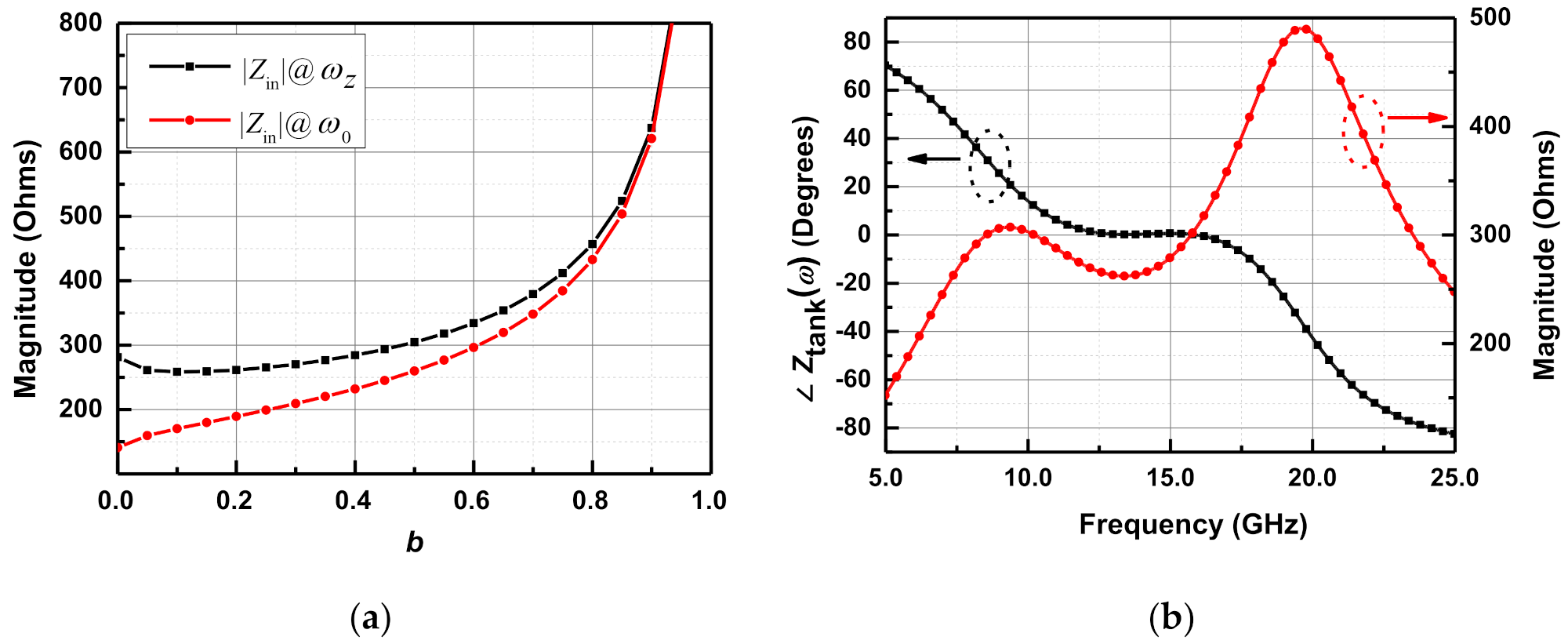
2.3. Magnitude Response

To sustain the waveform in the oscillator, the gain condition should also be satisfied. The tank impedance should be high enough to be easily compensated for by the negative resistance of the cross-coupled pair in the oscillator. A higher tank impedance means a lower current consumption and a higher output voltage amplitude. When ω = ωz,
Z in ( j ω ) ω = ω z = L p L s ω z 2 R p L p L s C p C s ( ω z 2 ω p 1 2 ) ( ω z 2 ω p 2 2 ) = 1 a R p C p C s ω z 2 = 1 R p ω z 2 C s 2
From (27), the magnitude of the tank impedance is inversely proportional to Cs when ωz is fixed. That is, relatively larger inductors and smaller capacitors are preferred to raise the tank impedance.
The zero-phase-shift plateau is present when the critical condition (23) is satisfied, and thus the magnitude at ωz is:
Z in ( j ω ) ω = ω z = 2 ( 1 b ) ( 1 b ) C s ω z = 2 ( 1 + b ) 2 ( 1 b ) C s ω z
If we define:
x = b ,   and   f ( x ) = ( 1 + x ) 2 ( 1 x )
d f ( x ) / d x = ( 1 3 x ) ( 1 + x ) 0 ,   when   x   1 / 3
Thus, the magnitude response of the tank at ωz exhibits a positive dependence on b when b ≥ 1/9.
The magnitude of the tank impedance at ω0 should also be considered:
Z in ( j ω ) ω = ω 0 = A cos ( δ ) B cos ( β ) = ω 0 2 R p C p C s ( ω 0 2 ω p 1 2 ) ( ω 0 2 ω p 2 2 )
Substitute (10), (11), (23), and (24), into (31),
Z in ( j ω ) ω = ω 0 = 1 2 ( 1 b ) C s ω z < Z in ( j ω ) ω = ω z
It is apparent from (32) that a larger b will improve the magnitude response at ω0, similar to the case at ωz. The magnitude of the tank at ωz and ω0 are plotted in Figure 6a, based on (28) and (32). With the increase of b, the magnitude rises slowly until b reaches 0.7. For a typical b within [1/3, 2/3], the variation of the magnitude is less than two times.
The phase response and magnitude response for the case shown in Figure 4 are plotted in Figure 6b The peaks in the magnitude response are located at ωp1 and ωp2, deviating from the zero-phase-shift plateau in the phase response. Thus, a waste of power consumption occurs, as compared to an LC-tank.

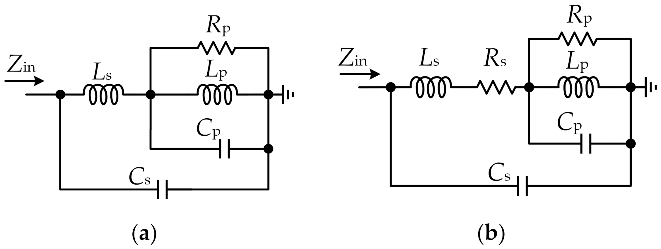
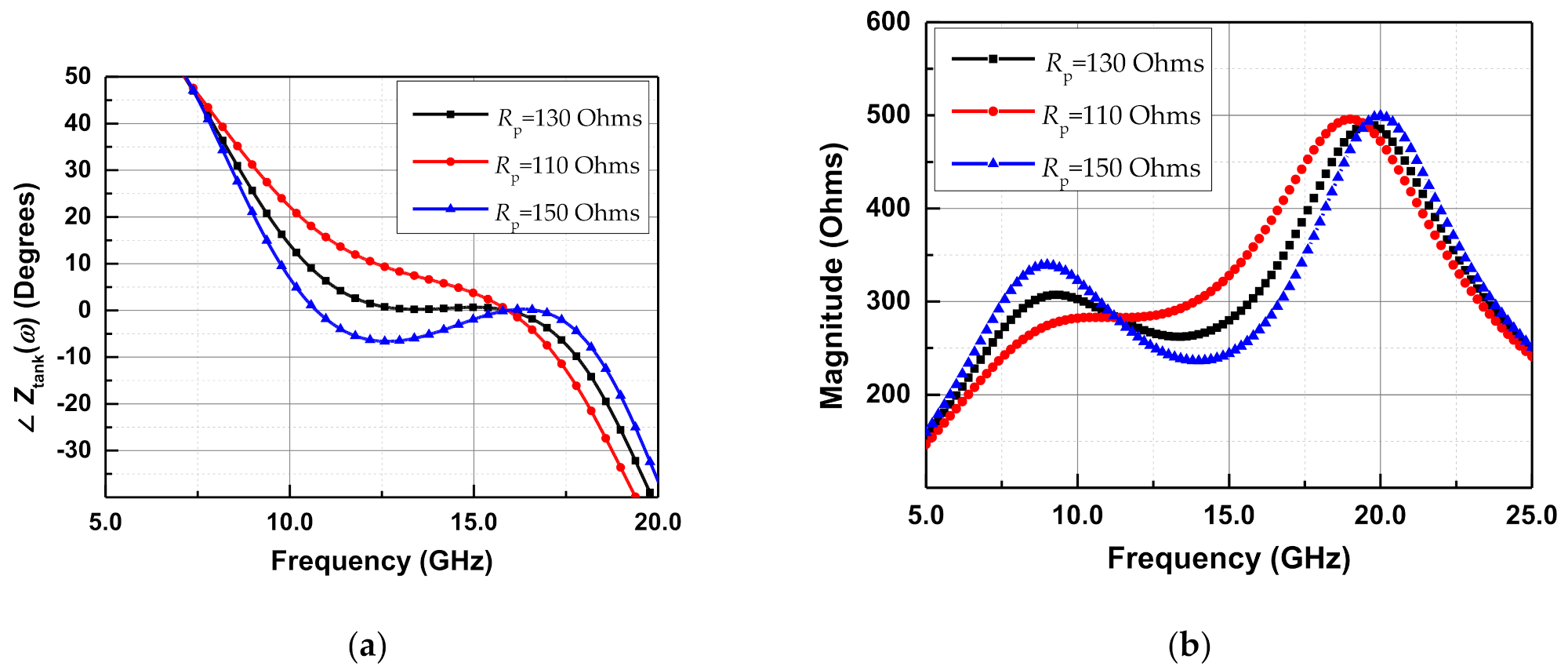
2.4. Influence of Rp and Rs

Referring to the tank shown in Figure 3a, the phase and magnitude responses versus Rp are plotted in Figure 7, where Lp, Ls, Cp, and Cs are 2 nH, 2 nH, 100 fF, and 50 fF, respectively. A zero-phase-shift plateau is achieved when Rp is 130 Ohms. A smaller Rp enables a sharper decline in the phase response, and a larger Rp may expand the locking range while increasing the in-band phase ripple. For the magnitude response, a larger Rp exhibits a lower in-band tank impedance. From this properly selected Rp of 130 Ohms, the quality factor Qp of the inductor Lp can be calculated. Assume the operating frequency to be 16 GHz, then:
Q p = R p 2 π f L p = 130 2 π × 16 × 2 = 0.65
This is quite a low-quality factor, such that a generally explicit resistor is needed instead of only exploiting the loss of the inductor Lp and capacitor Cp.
The loss of inductor Ls is modeled by a series resistor Rs. The phase and magnitude of Zin are shown in Figure 8. The loss of Ls generates a negative phase shift, but imposes little impact on the magnitude response of the zero-phase-shift plateau region. The negative phase shift generated by Rs can be easily compensated by adjusting Cp.
According to the analyses above, the design flowchart of the proposed ILFD can be outlined as follows:
Step 1. Choose a zero frequency ωz according to the frequency requirement;
Step 2. Determine Lp/Ls ratio according to the bandwidth requirement, and thus Cp/Cs is also determined;
Step 3. Determining the minimum value of the capacitor Cs according to the parasitic capacitance of the active devices (e.g., the cross-coupled NMOS pair and the injection transistor), and thus the values of Cp, Lp, and Ls are determined;
Step 4. Choose a proper value of the resistor Rp to obtain a wide-band zero-phase-shift plateau.
If a phase ripple may be tolerated, the resistor Rp may be chosen to be larger than the one in step 4.

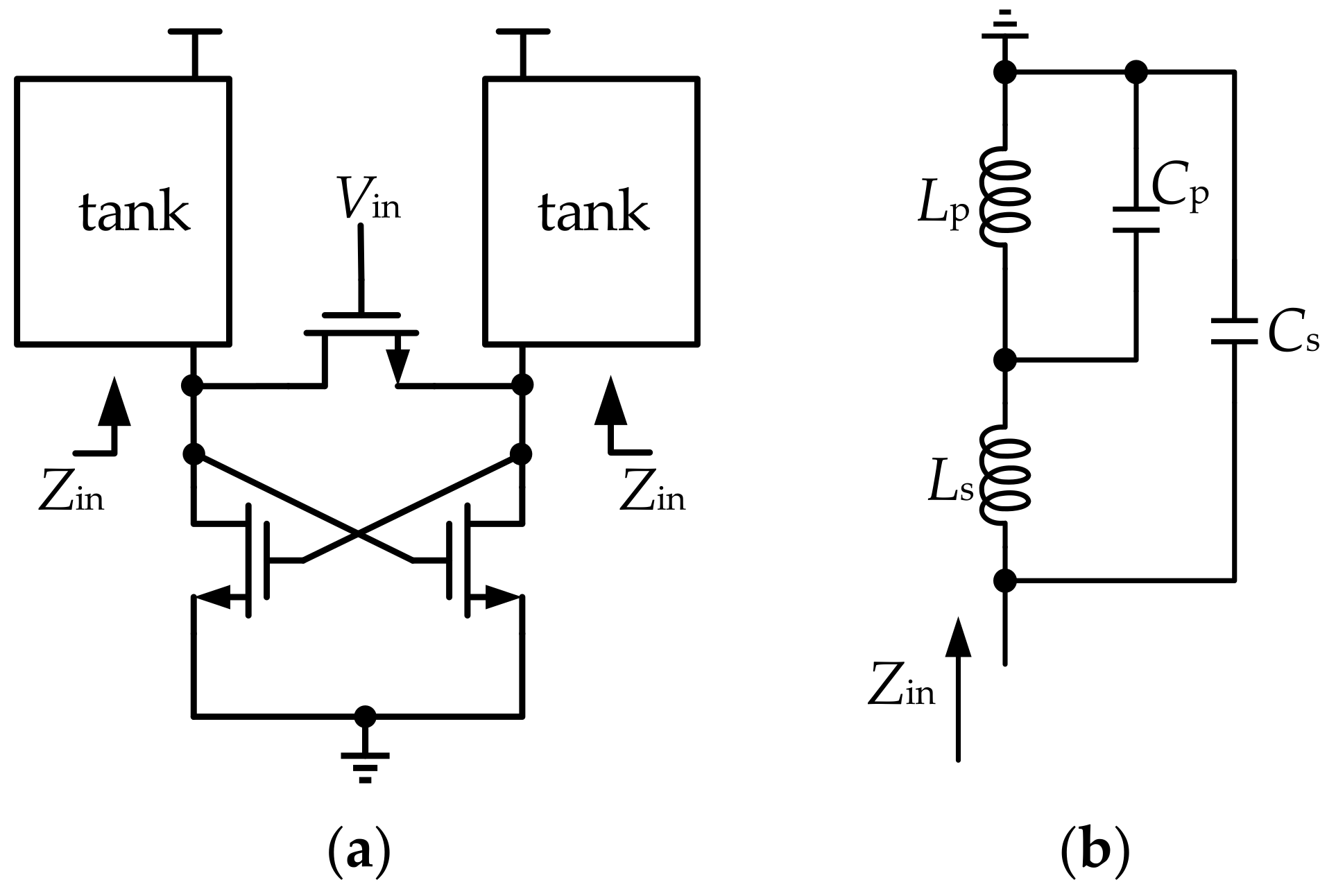
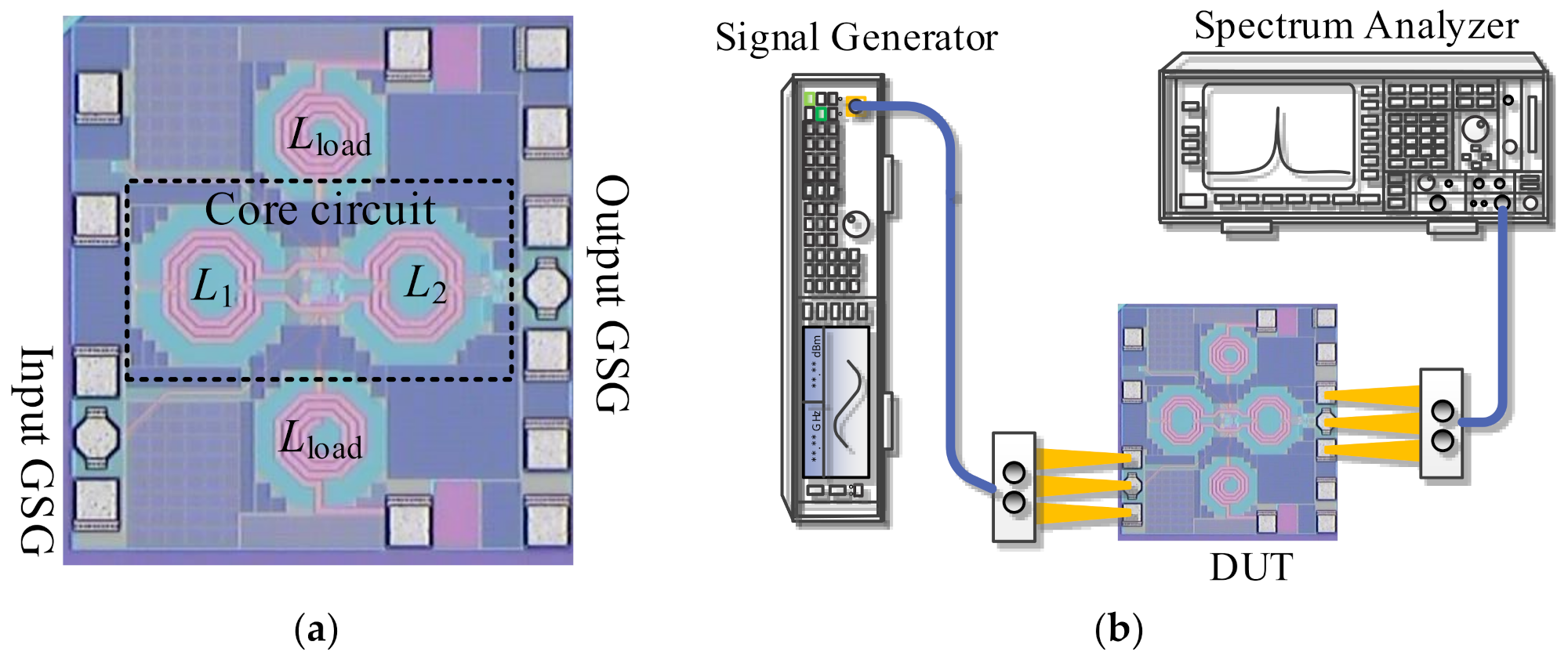
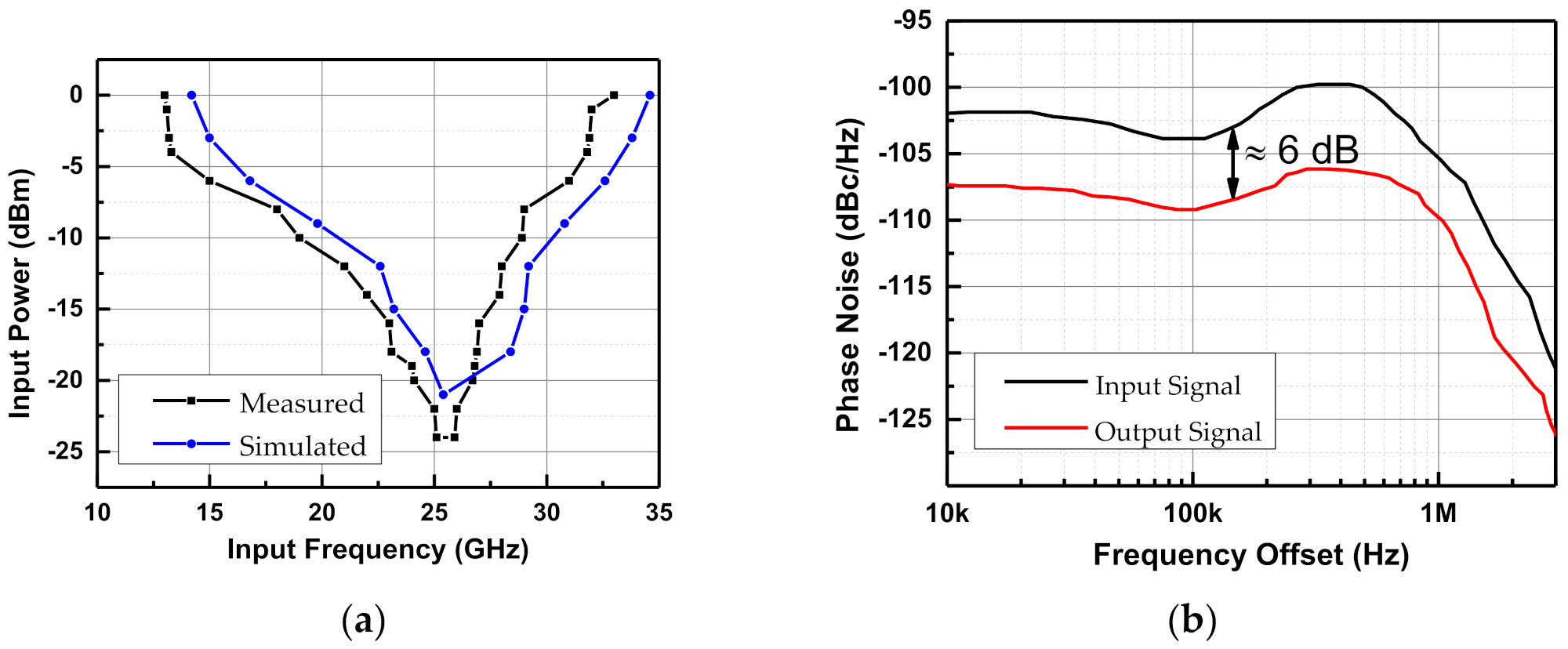
3. Implementations and Measurement Results

Figure 9 shows the circuit implementation of the proposed divide-by-2 ILFD. The core circuit of the proposed ILFD is composed of three NMOS transistors M1, M2, and Minj, and a dual-resonance tank. The cross-coupled transistors M1 and M2 form a negative resistance to compensate for the loss of the tank. The input signal is directly injected into the tank through the gate of the transistor Minj.
A differential inductor L1 is used as Lp, and a differential inductor with its center-tap split into two terminals is used as Ls. Though the inductors Lp and Ls are implemented as separate inductors for simplicity, the two inductors may be EM coupled to each other and form a transformer to save the area. A paralleled resistor R is used to increase the loss of the inductor L1. Except for the core circuit, the divide-by-2 ILFD also includes an output buffer to drive the 50 Ohms load of the spectrum analyzer. The output buffer is realized by a pseudo-differential common-source amplifier using inductors as loads.
The divide-by-2 ILFD is fabricated in the 65 nm 1P7M LP-CMOS process. The core area of the die photo shown in Figure 10a is 0.5 mm × 0.22 mm. The measurement setup is shown in Figure 10b. The input signal is generated from a commercial Analog Signal Generator, and a GSG probe is used for signal injection. The output is captured with a GSG probe and characterized using a Spectrum Analyzer. The insertion losses of the coaxial cables and adapters have been calibrated.
The core circuit consumes a DC power of 7 mW under a supply voltage of 0.7 V. The free-running frequency of the ILFD is first measured. When no signal is injected, the ILFD oscillates at 12.56 GHz. Figure 11a shows the simulated and measured input sensitivity curves of the proposed divide-by-2 ILFD. When the injection power is 0 dBm, the ILFD obtains a locking range of 87.0%, from 13 GHz to 33 GHz. When the injection power is lowered to −6 dBm, the proposed ILFD still sustains a locking range of 69.6%, from 15 GHz to 31 GHz. When the injection power is reduced to −24 dBm, the locking range decreases to only 3.9%, from 25 GHz to 26 GHz.
The phase noise performances of the input signal and output signal are also measured through the spectrum analyzer, and the results are shown in Figure 11b. The phase noise of the output signal is approximately 6 dB lower than that of the input signal, which coincides well with the theoretical value.
Table 2 summaries the performance of the fabricated divde-by-2 ILFD, and compares it with some other works.

4. EM Coupling Discussion

The inductors Lp and Ls may be EM-coupled to save the area. Referring to Figure 12a, the coupling factor of the two inductors is k, and the AC current flowing through Lp and Ls are ip and is, respectively. The equivalent model of Figure 12a is shown in Figure 12b, where:
L pe = L p + i s i p M ,   L se = L s + i p i s M
i s = i p + i p s L p / ( 1 s C p )
L pe = L p + ( 1 ω 2 L p C p ) M ,   L se = L s + M 1 ω 2 L p C p
Thus, the EM coupling can be decoupled, and the equivalent inductors Lpe and Lse can be derived following (36). Figure 12c shows the magnitude and phase response of the tank based on Figure 12a, where Lp, Ls, Cp, Cs, Rp, and k are 1 nH, 1 nH, 105 fF, 40 fF, 70 Ohms, and 0.3. It can be concluded that the EM coupling is possible to gain the same wide zero-phase-shift plateau while occupying a smaller area.

5. Conclusions

A wide-band divide-by-2 ILFD based on a distributed dual-resonance tank is reported. Based on the dual-resonance high-order tank, when the injection power is 0 dBm, the proposed ILFD obtains an ultra-wide locking range of 87.0%, from 13 GHz to 33 GHz, while consuming 7 mW from a 0.7 V power supply. When the injection power is lowered to −6 dBm, the proposed ILFD still sustains a locking range of 69.6%, from 15 GHz to 31 GHz.

Author Contributions

Conceptualization, Z.X.; methodology, Z.X.; software, Z.X.; validation, Z.X.; formal analysis, Z.X.; investigation, Z.X.; resources, Z.X.; data curation, Z.X.; writing—original draft preparation, Z.X.; writing—review and editing, Z.X. and K.K.; visualization, Z.X.; supervision, Y.Y. and K.K.; project administration, Y.Y.; funding acquisition, Y.Y. and K.K. All authors have read and agreed to the published version of the manuscript.

Funding

This work is funded by the National Key R and D Program of China [(Grant No. 2020YFB1805003, 2019YFB1706802)], and National Natural Science Foundation of China [(Grant No. 61931007, 62025106)].

Conflicts of Interest

The authors declare no conflict of interest.

References

  1. Hui, W.; Hajimiri, A. A 19 GHz 0.5 mW 0.35/spl mu/m CMOS frequency divider with shunt-peaking locking-range enhancement. In Proceedings of the 2001 IEEE International Solid-State Circuits Conference. Digest of Technical Papers. ISSCC (Cat. No.01CH37177), San Francisco, CA, USA, 7 February 2001; pp. 412–413. [Google Scholar]
  2. Tiebout, M. A CMOS direct injection-locked oscillator topology as high-frequency low-power frequency divider. IEEE J. Solid-State Circuits 2004, 39, 1170–1174. [Google Scholar] [CrossRef]
  3. Takatsu, K.; Tamura, H.; Yamamoto, T.; Doi, Y.; Kanda, K.; Shibasaki, T.; Kuroda, T. A 60-GHz 1.65 mW 25.9% locking range multi-order LC oscillator based injection locked frequency divider in 65 nm CMOS. In Proceedings of the IEEE Custom Integrated Circuits Conference 2010, San Jose, CA, USA, 19–22 September 2010; pp. 1–4. [Google Scholar]
  4. Mangraviti, G.; Khalaf, K.; Parvais, B.; Vaesen, K.; Szortyka, V.; Vandersteen, G.; Wambacq, P. Design and Tuning of Coupled-LC mm-Wave Subharmonically Injection-Locked Oscillators. IEEE Trans. Microw. Theory Tech. 2015, 63, 2301–2312. [Google Scholar] [CrossRef]
  5. Lai, W.-C.; Jang, S.-L.; Huang, Y.-W.; Juang, M.-H. Divide-by-2 Injection-Locked Frequency Divider Using 3-path Transformer-Coupled Resonator. In Proceedings of the 2020 27th IEEE International Conference on Electronics, Circuits and Systems (ICECS), Glasgow, UK, 23–25 November 2020; pp. 1–4. [Google Scholar]
  6. Zhang, J.; Liu, H.; Wu, Y.; Zhao, C.; Kang, K. A 27.9–53.5-GHz transformer-based injection-locked frequency divider with 62.9% locking range. In Proceedings of the 2017 IEEE Radio Frequency Integrated Circuits Symposium (RFIC), Honolulu, HI, USA, 4–6 June 2017; pp. 324–327. [Google Scholar]
  7. Chao, Y.; Luong, H.C. Analysis and Design of a 2.9-mW 53.4–79.4-GHz Frequency-Tracking Injection-Locked Frequency Divider in 65-nm CMOS. IEEE J. Solid-State Circuits 2013, 48, 2403–2418. [Google Scholar] [CrossRef]
  8. Jiang, Q.; Pan, Q. Tuning-less injection-locked frequency dividers with wide locking range utilizing 8th-order transformer-based resonator. In Proceedings of the 2021 IEEE Radio Frequency Integrated Circuits Symposium (RFIC), Atlanta, GA, USA, 7–9 June 2021. [Google Scholar]
  9. Mahalingam, N.; Ma, K.; Yeo, K.S. A Multi-Mode Multi-Coil Coupled Tuned Inductive Peaking ILFD for Low Injected Power with Compact Size. IEEE Access 2019, 7, 59059–59068. [Google Scholar] [CrossRef]
Figure 1. Phasor diagram for the current flown into the tank. (a) A general case. (b) The case when the maximum locking range is reached.
Electronics 11 00506 g001
Figure 2. (a) Conceptual diagram of the proposed ILFD. (b) AC equivalent circuit of the tank (losses of the inductors and capacitors not considered).
Electronics 11 00506 g002
Figure 3. AC equivalent circuit of the tank. (a) Taking Rp into consideration. (b) Taking Rp and Rs into consideration.
Electronics 11 00506 g003
Figure 4. Calculated phase response for the tank based on Figure 3a, wherein Lp and Ls are both 2 nH, Rp is 130 Ohms, and Cp and Cs are 100 fF and 50 fF, respectively.
Electronics 11 00506 g004
Figure 5. Simulated phase responses of the tank shown in Figure 3a, with Ls/Lp = 0.5, 1, and 2, respectively. (a) Phase response. (b) Magnitude response.
Electronics 11 00506 g005
Figure 6. (a) Magnitude plots of the tank impedance at ωz and ω0 versus b. (b) Phase (black) and magnitude (red) responses of the tank are shown in Figure 3a, where Lp, Ls, Cp, Cs, and Rp are 2 nH, 2 nH, 100 fF, 50 fF, and 130 Ohms, respectively.
Electronics 11 00506 g006
Figure 7. (a) Phase responses according to variations of Rp. (b) Magnitude responses according to variations of Rp.
Electronics 11 00506 g007
Figure 8. Loss of the inductor Ls is taken into consideration based on the tank in Figure 3b. (a) Phase responses of the tank. (b) Magnitude responses of the tank.
Electronics 11 00506 g008
Figure 9. Circuit implementations of the proposed ILFD.
Electronics 11 00506 g009
Figure 10. (a) Die photo of the proposed ILFD. (b) Measurement setup.
Electronics 11 00506 g010
Figure 11. (a) Simulated and measured input sensitivity curve of the proposed ILFD. (b) Measured phase noise performance.
Electronics 11 00506 g011
Figure 12. (a) AC equivalent circuit of the tank when the EM coupling between Lp and Ls is considered. (b) An equivalent model of (a). (c) Magnitude and phase response of the tank with the EM coupling taken into consideration, where Lp, Ls, Cp, Cs, Rp, and k are 1 nH, 1 nH, 105 fF, 40 fF, 70 Ohms, and 0.3, respectively.
Electronics 11 00506 g012
Table 1. Parameter list for the tank shown in Figure 3a.
Lp/HLs/HCp/FCs/FRp/OhmsLs/Lpabω1/Hzω2/Hzω0/Hz
Case 14n2n75f50f1460.52/31/39.19 G15.9 G12.1 G
Case 22n2n100f50f13011/21/211.3 G15.9 G13.4 G
Case 31n2n150f50f11221/32/313.0 G15.9 G14.4 G
Table 2. Performance summary and comparison.
Reference[6][7][8][9]This Work
Process65 nm CMOS65 nm CMOS40 nm CMOS65 nm CMOS65 nm LP-CMOS
Injection Power (dBm)00−4−50
Supply Voltage (V)10.80.91.20.7
Power Dissipation (mW)5.82.95.83.77
Locking Range27.9–3.5 GHz
(62.9%)
53.4–79.4 GHz
(39.2%)
28.8–91.9 GHz
(104.5%)
58 GHz
(18.3%)
13–33 GHz
(87.0%)
FoM * (GHz/mW)4.418.9710.92.872.86
Core Area (mm2)0.180.1260.020.0290.11
* FoM = locking range (GHz)/power dissipation (mW).
Publisher’s Note: MDPI stays neutral with regard to jurisdictional claims in published maps and institutional affiliations.

