1. Introduction
Nano-scale SOI optical interconnects, comprised of silicon/silicon-dioxide (Si/SiO
2) dielectric waveguides operating at 100s of terahertz (THz), constitute an increasingly important building block of modern integrated circuits, where the high-tech market demands smaller form-factors and wavelengths. Considering the non-ideal manufacturing process, random imperfections in the surfaces of nano-scale dielectric waveguides may cause significant signal degradation and power attenuation, as EM waves propagate through the interconnect structure, where the loss is primarily due to EM wave scattering with surface roughness of the waveguide [
1,
2,
3,
4,
5]. Therefore, the characterization of scattering loss is a topic of significant interest to the scientific community [
1,
2,
3,
4,
5,
6,
7,
8,
9,
10].
The three-dimensional (3D) structure of SOI optical interconnects poses certain challenges to its analytical and numerical modeling; thus, the stochastic scattering loss observed in nano-scale THz SOI interconnects is often approximated using 2D planar models of the dielectric slab waveguide exhibiting surface roughness. The 2D analogue is useful for analytically [
5,
8,
10] characterizing the effect of scattering loss on the power attenuation of light waves, and is used as a comparison for both experimental analysis (of physical waveguides) [
1,
2,
3,
4] and numerical analysis [
1,
2,
6,
7,
9].
In 1983, Kuznetsov and Haus [
11] published their work on using the 3D volume current method (VCM) to evaluate the radiation loss in dielectric waveguide structures. Their work includes analysis of single-line, two-line coupled, and three-line coupled waveguide structures, in the absence of random surface roughness. In 1990, Lacey and Payne [
5] released their seminal work analyzing 2D planar waveguides exhibiting random surface roughness for a single-line waveguide structure. Their work applies Green’s functions to the structure, operating in the transverse-electric-to-z (TE
z) mode, as an approximation for scattering loss in 3D optical interconnects, and later in 1994 [
8] it was updated to use normalized waveguide parameters. In 2005, Barwicz and Haus [
6] expanded on both of those developments by applying the 3D VCM to single-line waveguides exhibiting random surface roughness. In each of these cases, despite having relatively simple geometries, the solutions are formulated around complicated integral equations, and the solutions only become more complicated as the geometry becomes more complex, for example by adding roughness, multiple tightly-coupled lines, arbitrary-shaped lines or grating, etc., thus limiting the application of integral-based solutions. An effective workaround to the integral-equation complication is to reformulate the problem around differential-equations, leading to the FDTD method. A version of the FDTD method based on wavelets is used in [
2], but the details of the FDTD formulation are not included. The FDTD method is also used in [
1] through the software tool
Lumerical, but again details of the FDTD methodology are absent.
The major contributions of the present work are as follows. (
1) We provide the FDTD methodology for analysis of 2D dielectric waveguides exhibiting random surface roughness, operating in the TE
z mode. (
2) We propose a methodology for the extraction of S-parameters, and we apply that methodology to the characterization of scattering loss. (
3) We improve the computational efficiency of this model by using filtering techniques to attenuate numerical noise from simulation results, thereby allowing for the use of a relatively coarse spatial and temporal discretization while retaining the integrity of numerical results. (
4) While the integral-based VCM has increasing complexity as the geometry becomes more complex, the FDTD method is especially well-suited for arbitrary waveguide geometries and arbitrary surface roughness profiles. To keep this presentation simple and concise, we chose to apply the methodology to a single line; however, it can easily be adapted to multiple tightly-coupled lines. (
5) We provide the Python [
12] code titled
Optical Interconnect Designer Tool (OIDT) [
13] which features multi-CPU-core support for parallelized FDTD, as an open-source software package [
14] hosted on GitHub through a public repository under the GNU GPL v3.0 license [
15], to encourage further exploration and (inter)national collaboration on optical interconnect research.
While the FDTD method implemented via a
serial programming paradigm would be computationally expensive, its highly
parallelizable nature may provide a potential path to a computationally expedient solution; thus, herein we begin to explore this potential by developing a parallelized implementation of FDTD with a traditional Yee-based algorithm [
16,
17] and convolution perfectly matched layer (CPML) [
18] boundaries, to characterize the scattering loss in dielectric slab waveguides exhibiting surface roughness.
The remainder of this paper is organized as follows.
Section 2.1 outlines the physical waveguide structure analyzed throughout this paper.
Section 2.2 establishes the details of the FDTD model being used, where
Section 2.2.1 provides additional details on the discretization and application of random roughness profiles to the FDTD environment.
Section 2.2.2 details the filtering technique used to improve numerical measurements from FDTD simulations.
Section 2.2.3 addresses the coordinate transformations used to move between the analytical solution and the FDTD model. In
Section 2.3, we provide the methodology for S-parameter extraction in 2D FDTD. In
Section 2.3.2, we formulate the relations between the S-parameter matrix and the scattering loss
. In
Section 2.4, we propose an updated equation for computing the stochastic scattering loss
based on physically realistic waveguide parameters and define its components, including a discussion on the exponential ACF. In
Section 2.5, we validate the FDTD model by correlating against analytical expressions for the wave impedance, the propagation constant, and the ideal S-parameter matrix. In
Section 3, we discuss the numerical results of FDTD, and the potential sources of error between FDTD and the analytical model. In
Section 3.1, we compare our results against those of other investigators. In
Section 3.2, we examine the dependence of
on input power and formulate the mode normalization
. We conclude with closing remarks in
Section 4.
2. Methods
2.1. The Waveguide Structure
Optical interconnects are comprised of spatially 3D waveguide structures with a certain surface roughness profile which may not vary much relative to the smooth (flat) waveguide’s width. Often, 2D models of dielectric slab waveguides with the same height and similar material parameters are used to analyze the 3D waveguide. This allows the analysis to be decomposed into two modes: (1) transverse electric (TE) and (2) transverse magnetic (TM).
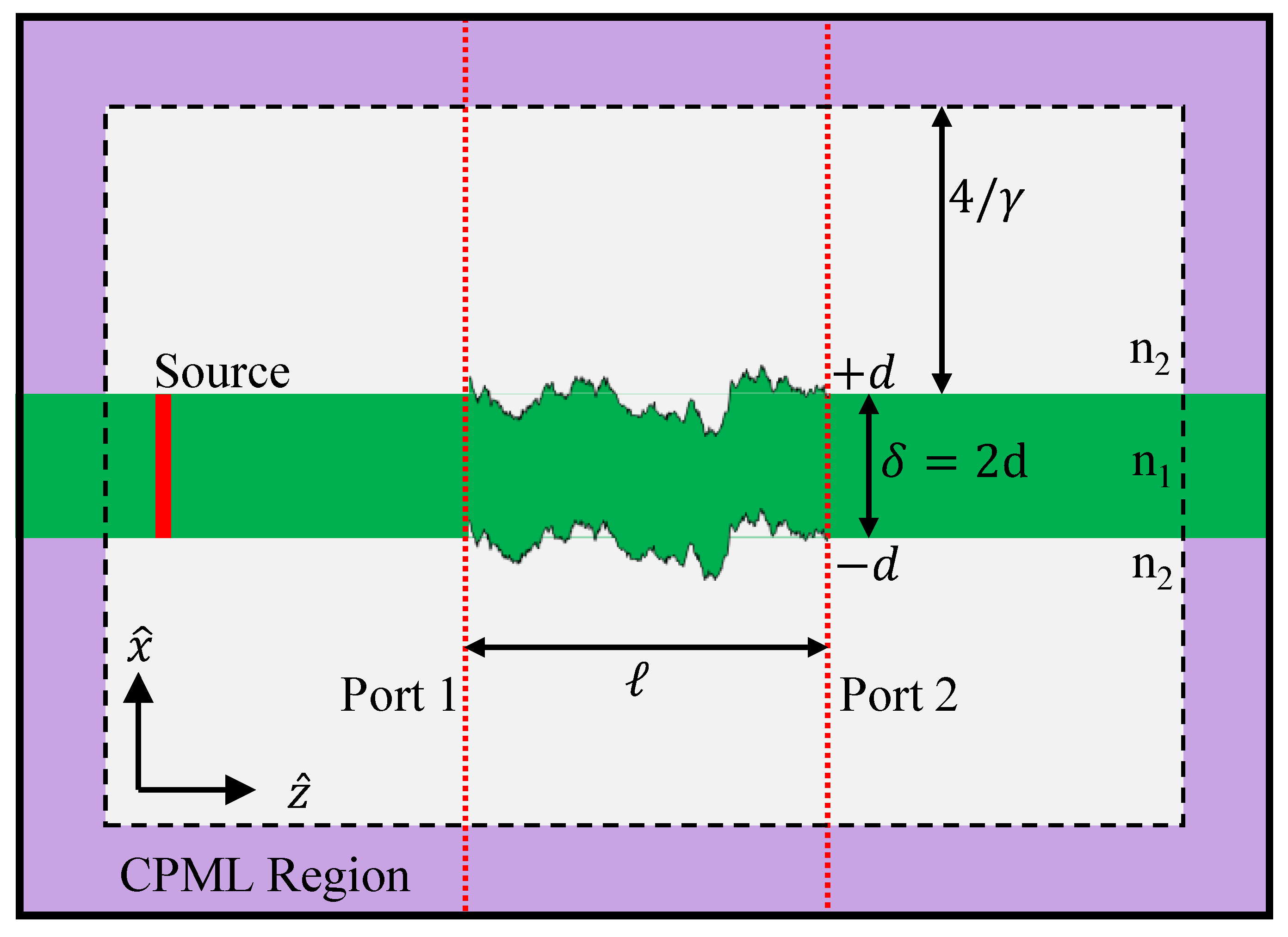
Here, we analyze the structure in
Figure 1 for the TE mode. We start by defining the coordinate grid in the
-
plane, and orient the device to operate with infinite extent in both the
and the
directions, where the waveguide length and power flow are along
and the waveguide height is infinite along
.
The dielectric slab waveguide consists of two regions, the
core and the
cladding. The core has a refractive index of
, and the cladding has a refractive index of
, where
. The core region has a finite nominal width, which is typically denoted as two half-widths. Here, the width is
, where
d is the half-width used throughout this work. The fields in the waveguide are assumed to be
time harmonic (with
dependence, where
(rad/s) is the angular frequency) in nature with the E-field taking the form in (
1).
where
(rad/m),
is the effective index found via the effective index method (EIM) [
10],
is the free-space wave number,
is the attenuation constant resulting from sidewall roughness, and
is a piece-wise function with its components defined in (
2)–(
4). In (
2) the term
is a scaling constant.
Random perturbations exist along the boundary between the core and cladding, resulting in the
surface roughness profile. We use an
exponential ACF to describe the surface roughness by its standard deviation
and its correlation length
. The
mean of the profile is 0, so the random perturbations are not included in the nominal width. We further assume the cladding extends infinitely outward from the core region. The FDTD environment used in this paper is described fully in [
7,
14,
19], and in
Section 2.2.
2.2. The FDTD Environment
The nominal waveguide structure may expediently fit into 2D FDTD analysis. We start by converting the nominal structure into uniform discrete cells with side length
. The temporal resolution is then set at the
Courant stability limit [
20] for 2D FDTD, where the background material is set to the cladding medium. We apply the CPML [
18] to the exterior of the computational domain, thereby simulating infinite space with minimal reflections and computational cost.
We define a length ℓ over which we generate and discretize a random profile; the remaining FDTD cells create an extra buffer space to allow for modal waves to settle, after leaving the source point and before reaching the recording (numerical measurement) point. Each source and recording location are designated by a separate port, e.g., a single optical line would be characterized by two ports, with one port at each end of the line.
Once the roughness profile is ready, it is applied as the core and cladding boundary between ports. Referring to
Figure 1, we place a source condition along
in a vertical line of cells across the entire opening of the waveguide, where the distance between the source and CPML is more than 10 cells, while we may approximate infinite space with the CPML, we still need to retain a buffer space in the cladding between the waveguide and the CPML boundary. To capture the intricacies of the interactions of the EM fields in both the core and cladding regions, we need to set the cladding size appropriately. Therefore, it is necessary to capture as much of the E-field as possible. Note, in (
2) the E-field magnitude decays exponentially in the cladding region with a rate of
, and we can use that behavior to set the cladding buffer size. At a distance of
from the core/cladding boundary, the E-field magnitude at the edge of the simulation space is no more than 2% of the E-field magnitude at the core/cladding interface, and it only decays further from there; thus, the cladding region size is set accordingly, as in
Figure 1.
Data are collected in the form of E-field values at ports 1 and 2 along the first line of cells adjacent to the rough region. These points are recorded at each time-step for the duration of the FDTD analysis. In post-processing, we take the recorded time-domain E-field values and convert them to the frequency domain with the fast Fourier transform (FFT) [
21]. We then numerically integrate the E-field over the recorded line of cells, resulting in a frequency dependent voltage with which further analysis may be performed.
We set up the FDTD grid based on the waveguide geometry, material parameters, and desired frequency range. The geometry is set up as shown in
Figure 1, where
and
. We additionally set the fundamental frequency as
THz (corresponding to source wavelength
m). Using the core refractive index, we find the minimum phase velocity
(m/s). Using the fundamental frequency, we assign our desired maximum frequency as
(Hz), where
is the number of desired harmonics above the fundamental. Using both the minimum phase velocity and the maximum frequency, we find the minimum wavelength simulated in the FDTD scheme with
. Then, our spatial discretization is
. At
,
nm/cell. We set the time-step
at the Courant limit based on the cladding material which has the largest possible phase velocity in the FDTD environment, such that
.
The total grid is 5554 cells × 247 cells () with 26,997 time-steps. We use 40 layers of CPML as the absorbing boundary condition because in our experience 30–40 CPML layers provides good correlation of wave impedance within 1%. Along , the core region is centered and the nominal full width measures 36 cells, where the remaining 300 cells are evenly distributed on either side of the core as cladding. Along , cells, and the remaining 1858 cells are evenly distributed to each port region.
The computations are done by using a workstation with two Intel® Xeon® E5-2687W v3 CPUs (40 logical cores), operating at 3.10 GHz. Each simulation occupies less than 410 MB of RAM and is completed in roughly 300 s (or 5 min).
2.2.1. Verifying the Validity of Discretized Roughness Profiles
We start by assigning a target for
,
, and
, where
designates the
mean in this subsection. These parameters are then normalized by the spatial discretization step-size
value used in the FDTD simulation to yield
. The discrete values are passed into the
Pyspeckle [
22] Python library which uses the methods in [
23] to generate random profiles; this generation process returns an array of a specified size with floating point values quantifying the surface perturbation. As was the case in [
7], a linear offset is added to the aforementioned floating point array to ensure that all values are positive. The offset array is then cast to integer values via the
floor function and the same linear offset is subtracted from the now integer array, where the final discrete array has parameters
,
, and
. The error between input (
) and output (
) parameters may be quite large, due to the discretization process. However, we may circumvent this issue by constraint-based generation of profiles, described below.
We set a percentage tolerance for the normalized input parameters and we check that the output parameters fit the input parameters within the prescribed tolerance. If a profile does not meet the criteria it is discarded and a new profile is generated. In our numerical experiments, the tolerance is specified by and , and .
We find
and
via built-in Numpy functions
std and
mean, respectively. We may estimate the
value that fits the autocorrelation data, as explained next. We start by finding the autocorrelation of the generated discretized surface profile using the Pyspeckle
autocorrelate function which provides a normalized array with its maximum value occurring at
. Note the autocorrelation of the generated profile tracks an exponential ACF up to the correlation length, as can be seen in
Figure 2. With that in mind, we apply a root finding technique to determine
while using
as the reference value. We then subtract
from the discrete ACF and find the root closest to
, which is the correlation length of the discrete ACF. We may then compare the
with
to determine the validity of the generated discretized profile.
For samples with parameter values nm and nm, and knowing that the probability distribution function (PDF) of the random process is normal in nature, we know that 99% of values in the final array will be contained in the range . Applying the floor function to this range results in the discrete set which may cause significant differences between output values and input values .
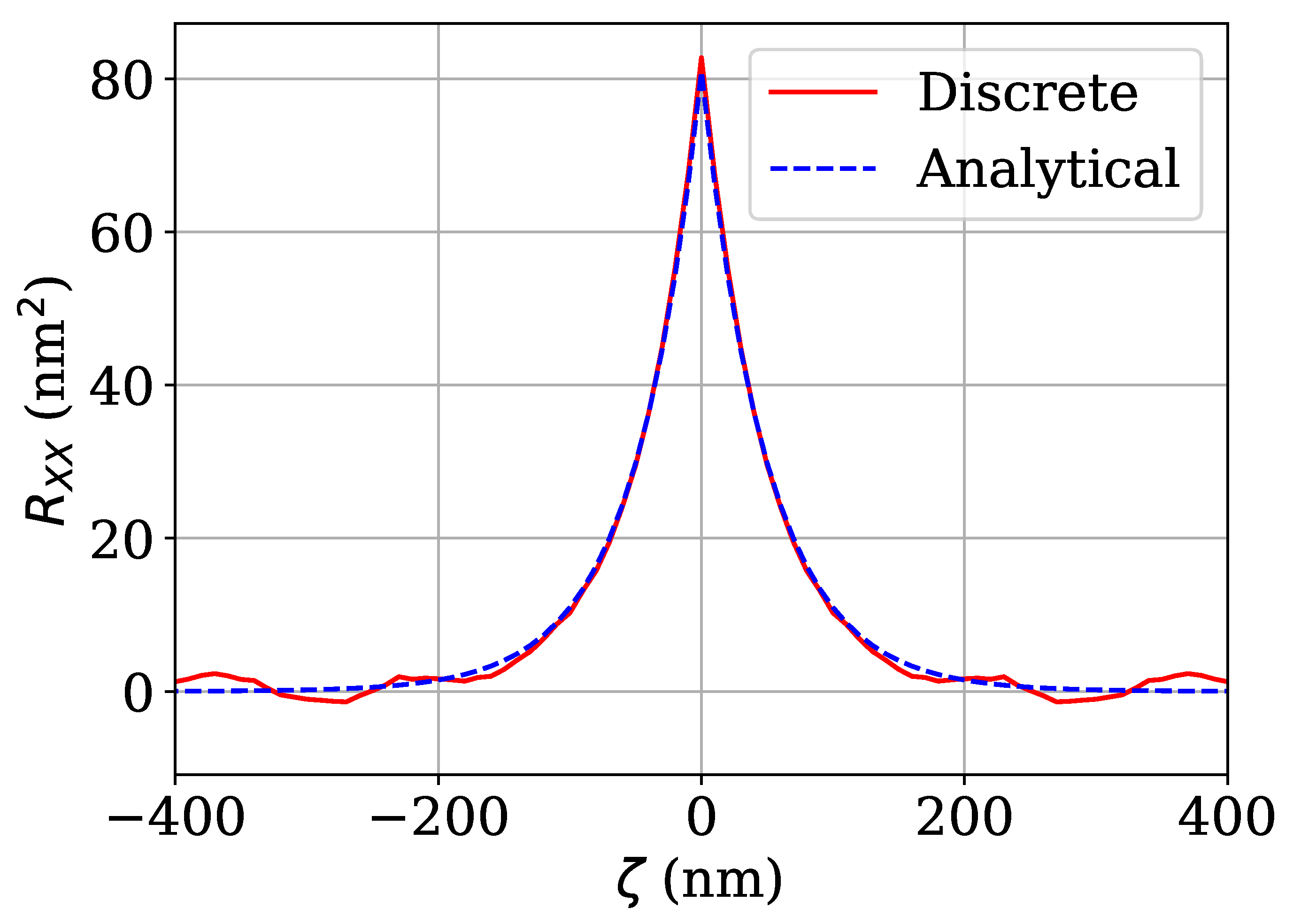
Figure 2 compares a discretized exponential ACF comprised of 5000 samples against the continuous analytical (
18). Even at this small sample size, the discretized profile still correlates well to the ideal ACF up to
, but after that point, there is noticeable noise. At
nm the discretized and continuous analytical ACFs do not line up perfectly. The misalignment at
nm may be remedied by normalizing the analytical ACF to match the discretized ACF, using
instead of
.
2.2.2. FDTD Noise Reduction
Numerical experiments involving waveguides with random surface roughness result in a certain amount of noise in
. We may observe that in the initial calculation, labeled unfiltered, there is rapid oscillation around the trend; such oscillations are undesirable and cause scattering loss readings to vary between numerical experiments. This issue may be resolved by the use of a
moving-average function over the frequency range of interest; this technique is often used to reduce noise levels in digital signals [
24]. We use (
5) to reduce the noise level at each frequency point, where
N is the number of samples to either side the reference index
k.
The rolling average function is effective at reducing noise levels, but due to the smoothing effect it also introduces its own set of numerical distortions. However, the introduced error is small when N is small. As such, we use to generate the filtered curve, where the rapid oscillations have been reduced but the trend remains mostly unchanged.
2.2.3. Modal Transformations and Coordinate Mapping
The geometry used for the characterization of scattering loss from random surface perturbations, shown in
Figure 1, is based on the geometry from Figure 5 in [
10]. The fields in [
10] are described as TE
z, since
and
, and by using (56), (59), and (60) in [
10] we know the non-zero field components are
, while
. The TE
z field configuration may also be obtained from (6-72) in [
25] and setting
, and it is mathematically identical as two other modes; specifically, setting
in (6-64) in [
25] yields the TM
y, and in (6-74) in [
25] yields TE
x.
In our geometry of
Figure 1, there exists a single nonzero E-field component along the invariant (infinite) direction (
), and two nonzero H-field components along the finite directions (
,
) which may be interpreted as either height or width [
10]. Out of the three mathematically equivalent modes (TE
z, TM
y, TE
x), we choose the TE
z field configuration here, as it aligns best with the physical interpretation of the physical waveguide with propagation along
(length), a transverse E-field along
(width or height), and H-field components along
and
.
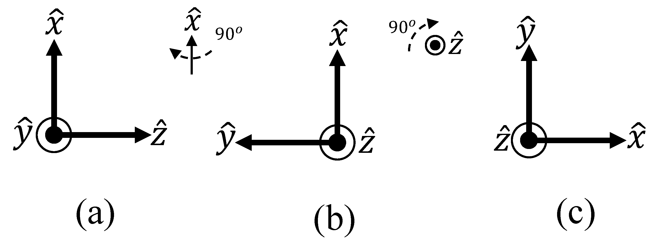
Our FDTD simulations are based on the traditional Yee algorithm in a 2D lattice, as formulated in ([
17], ch. 3). Our FDTD formulation is derived with the assumption that
and
, resulting in the TM
z mode with field components
. This FDTD lattice may initially appear to be in conflict with our analytic formulation; however, note that the E-field has a single nonzero component along the infinite (invariant) direction, and the H-field has two nonzero components. Since we can assign the FDTD geometry in an arbitrary manner, we choose to orient
along the length and
along the width (or height), resulting in a field configuration with the same orientation as the analytical formulation but with a rotated coordinate grid. We can rotate the coordinate grid of the analytical field configuration such that it results in a configuration
identical to the FDTD fields by the steps shown in
Figure 3.
In
Figure 3, starting with the analytical expression in (a), we rotate the coordinate grid twice. The first rotation is 90
around
from
toward
; this produces the grid in (b). The second rotation is 90
around
from
to
; this produces the grid in (c). The mapping is complete after these rotations, and we can then use the FDTD 2D TM
z field components
to represent the analytical 2D TE
z field components
, respectively, with no modifications to the established FDTD formulation nor the analytical formulation.
2.3. S-Parameters Extraction Methodology in FDTD
S-parameters are often used to characterize a variety of electronic systems [
7,
19,
26]. The methodology of finding S-parameters may be applied to 2D FDTD simulations quite expediently [
7,
19].
We use the traditional definition of S-parameters [
26], where the
total voltage wave measured at each port in a system can be decomposed into
incident and
reflected waves, i.e.,
, and those components can be used to evaluate S-parameters as in (
6), where
are port numbers,
is the incident wave,
is the reflected wave, and
is the total wave.
In our FDTD simulations, we use a two-port system, so . This methodology may be further extended to systems with more than two ports.
2.3.1. Computing S-Parameters, Using FDTD
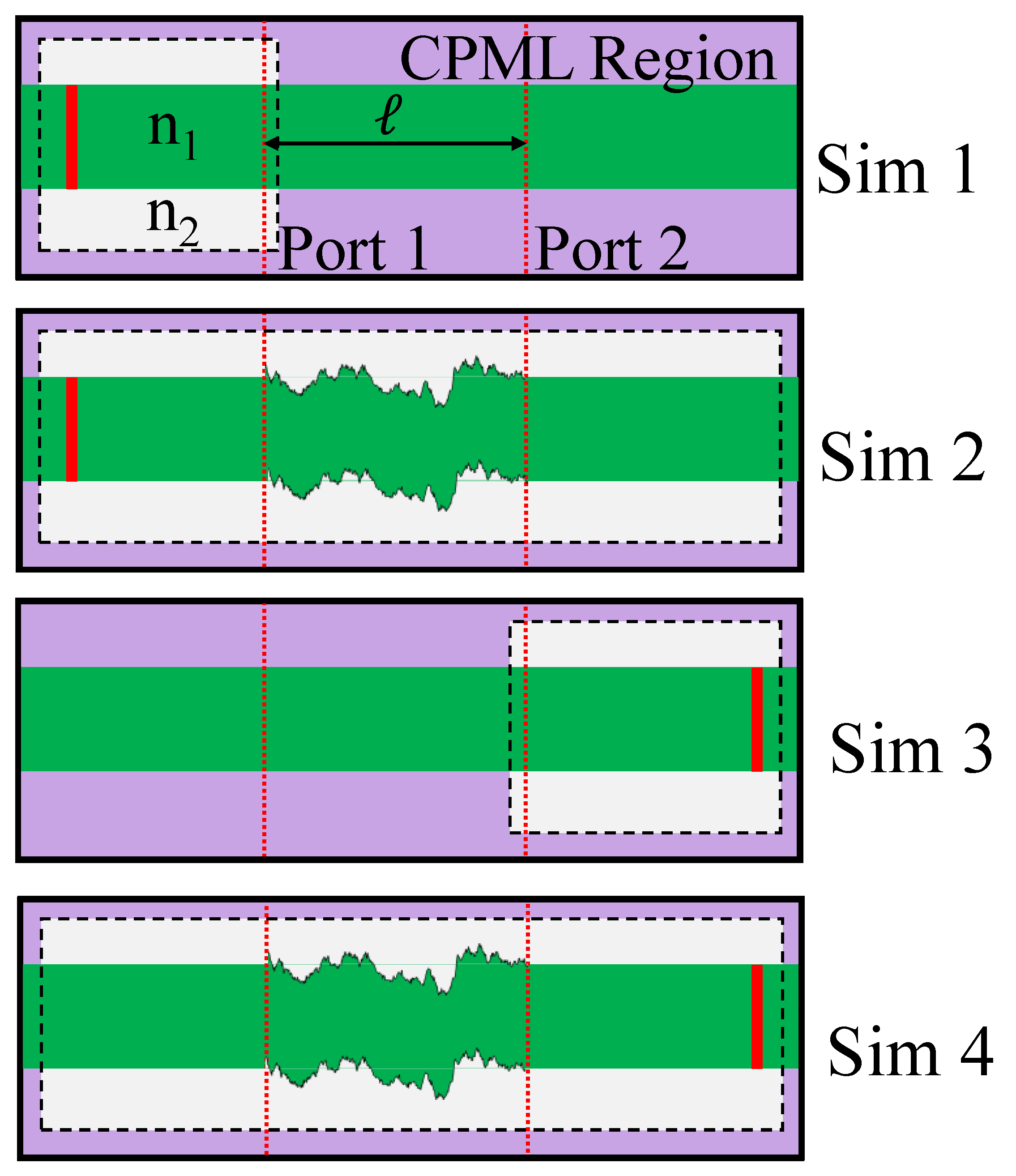
We are able to record total, incident, and reflected fields in FDTD simulations, but these may not all be recorded simultaneously. Therefore, we utilize a four-step simulation setup for collecting S-parameters.
Other simulations for calculation of loss may be considered a subset of the four-step simulation process [
19]. Each of the simulation steps are visualized in
Figure 4, and explained below. The
baseline setup and geometry is in
Figure 1.
Sim 1: The first simulation starts by placing the source condition at port 1, so for this simulation. We simplify the geometry of the dielectric slab by excluding the random sidewall perturbations at this time. Additionally, we extend the right-side CPML boundary to 10 cells to the right of port 1. This simulation results in .
Sim 2: The second simulation starts with the same source condition as simulation 1. We then apply a valid discrete roughness profile to top and bottom boundaries between core and cladding. In our simulations, we chose the top and bottom profiles to be identical, but other choices are possible too. The CPML boundaries are evenly distributed around the computational domain. This simulation results in and .
Sim 3: The third simulation is similar to the first simulation. We place the source condition at port 2, where in this simulation, and extend the left-side CPML boundary to 10 cells to the left of port 2. Simulation 3 results in .
Sim 4: The fourth simulation finalizes the port field data collection. Similar to the third simulation, we place the source condition at port 2, and similar to the second simulation we set the CPML boundaries at the baseline limits and apply the roughness profile in the same manner. This simulation results in and .
The fields recorded in the numerical experiments are limited to the four aforementioned steps, but there are still two field components missing which would fully describe the scattering matrix; those are when , and when . Here, we may use the decomposition relation to find the implicit reflected fields. Specifically, using from Simulation 1 and from Simulation 2, we may obtain . Similarly, we may recover from simulations 3 and 4.
With each of these values calculated from the numerical experiments, the S-parameters matrix may now be computed. In ideal waveguide with no sidewall perturbations, we would expect the S-parameters matrix (of the waveguide system) to be both
symmetric (
reciprocal) and
unitary (lossless) [
26]. For a waveguide with sidewall perturbations, we expect the S-parameters matrix (of the waveguide system) to be symmetric (reciprocal) but non-unitary (lossy) [
26]. Higher port numbers may be simulated by following the same process of incident field simulation followed by total field simulation, for each port subsequently.
2.3.2. Direct Method of Computing Scattering Loss, Using FDTD
Using the second simulation, we may find the total voltage wave values at both ports 1 and 2, but this time we label them and , respectively. We assume the voltages to have the same form as the electric field but with the element replaced with , i.e., . In this form, it may be observed that as z increases, we also expect the voltage to attenuate in amplitude and accumulate in phase.
Since we have measured the voltage at two port locations, we may determine the attenuation. To do this, we divide
by
, resulting in (
7).
Using (
7) we may isolate
by using the complex logarithm where
,
is the complex-domain natural logarithm of
z,
is the natural logarithm with base
e, and
is the true angle of
z; i.e., the angle of
z which includes all full turns and may have a magnitude greater than
[
27].
Applying (
8) to (
7) results in (
9).
Equation (
9) may be separated into real and imaginary components, resulting in the final expression in (
10), for calculating power loss directly from FDTD experiments.
While (
10) is possibly the most direct method for calculating power loss from FDTD simulation, there is an alternative definition which could accomplish that task through the use of S-parameters. We start by taking the argument of the natural logarithm in (
10) and squaring it, but instead of 0 and
ℓ being the reference points, the voltages are now in reference to ports 1 and 2, leading to
In (
11), we may replace the magnitude-squared operation with the equivalent complex operation, resulting in
where
denotes the complex conjugate operator.
Simplifying (
12), we may combine the incident and reflected voltage waves into compact S-parameters from. We may then reinsert
A into a natural logarithm and recover the expression for
as a function of S-parameters in (
13) [
19].
The form of
in (
13) may also be utilized on systems with larger number of ports. In this case, port 1 is used as the reference port for loss, but in general the reference port may be any port in a multi-port system. In a large multi-port system, the loss equation using S-parameters may be computed for each reference port.
2.4. Analytical Loss Function
In the ensuing formulation, we assume simple media; i.e., linear, isotropic, and non-dispersive. Following the recent work in [
10], we propose (
14) as the generic scattering loss function.
Equation (
14) is similar to the loss function used in previous works [
5,
8,
10], but we have made a modification by dividing
in those works by the normalization factor
.
Either part of the piece-wise function (
2) may be evaluated at
and result in (
15).
Note that
, derived in Equation (73) in [
10], is dependent on the input power. This dependency is not desirable; thus, it is eliminated by introducing the factor,
, in (
14), normalizing the amplitude of
, as explained in
Section 3.2.
The term
is defined with (
16).
The term
is defined with (
17) and represents the contribution by the surface roughness described by a random distribution.
where
is the power spectral density of the surface roughness profile.
Surface roughness may be approximated as a stationary random process [
10], therefore the power spectral density may be recovered through the ACF of the roughness profile, which may be assumed to have an
exponential shape [
4,
5]. The exponential ACF is given by (
18) [
10]
where
and
are the standard deviation and correlation length of the profile, respectively, and
is the spatial shift variable.
There are two observations that could be made about (
18) by setting
to specific values. First,
results in the variance of the profile. Second,
; this second result is used later for approximating the value of
from surface profile data generated by the
Pyspeckle software [
22]. Some photo-lithographic processes for Si/SiO
2 may lead to profiles with
nm and
nm [
4].
We define the spatial Fourier transform (SFT) as
where the input function is translated from
-space (m) to
k-space (rad/m),
k is the wave number, and the imaginary number
.
Applying the SFT (
19) to (
18), yields
We may insert (
20) into (
17) and numerically evaluate the integral to obtain the contribution of the surface roughness profile to the loss
.
2.5. FDTD Model Validation
We validate the FDTD model being used in these numerical experiments in three ways, described below. Unless stated otherwise, the data in this section is generated for a smooth waveguide with nm, , , and THz. Validation must be done prior to performing numerical experiments, so we utilize the smooth waveguide and the below methods for model validation. Using known and expected attributes of the smooth waveguide, we can compare the results obtained from numerical experiments to provide confidence in the validity of our model before performing numerical experiments with waveguides that exhibit surface roughness.
2.5.1. Wave Impedance
One such method is through comparison with a known analytical solution to the smooth dielectric slab waveguide. We use the wave impedance of an outward traveling wave. This solution is well established and has been derived in several places [
10,
25]. We find the wave impedance by dividing TE
z mode E-field by the corresponding H-field component along the length of the slab waveguide. Here, those fields are
and
, respectively. In the smooth slab case, the real portion of the wave impedance should be very small. For the analytical solution, the division between the E-field and H-field gives
where
is the magnetic permeability. Division of
x by its magnitude is used to set the appropriates sign for either above or below the slab.
The FDTD portion of this comparison may be conducted through the second simulation from
Section 2.3.1 with the surface roughness omitted. Since the wave impedance is calculated for an outward traveling wave, we use the E-field and H-field data in the cladding region. We take all the steps necessary to compare frequency-domain voltages as described in
Section 2.2, but we exclude the final integration such that we are left with field data for every point along the line at ports 1 and 2. Using the port 2 data allows for the wave to propagate over a long enough distance to be well-set into the lowest order mode. We take the measurements from two cells below the lowest core cell which leaves a single cell buffer between the core region and the cell used for this calculation. Finally, the imaginary component is compared to the analytical solution.
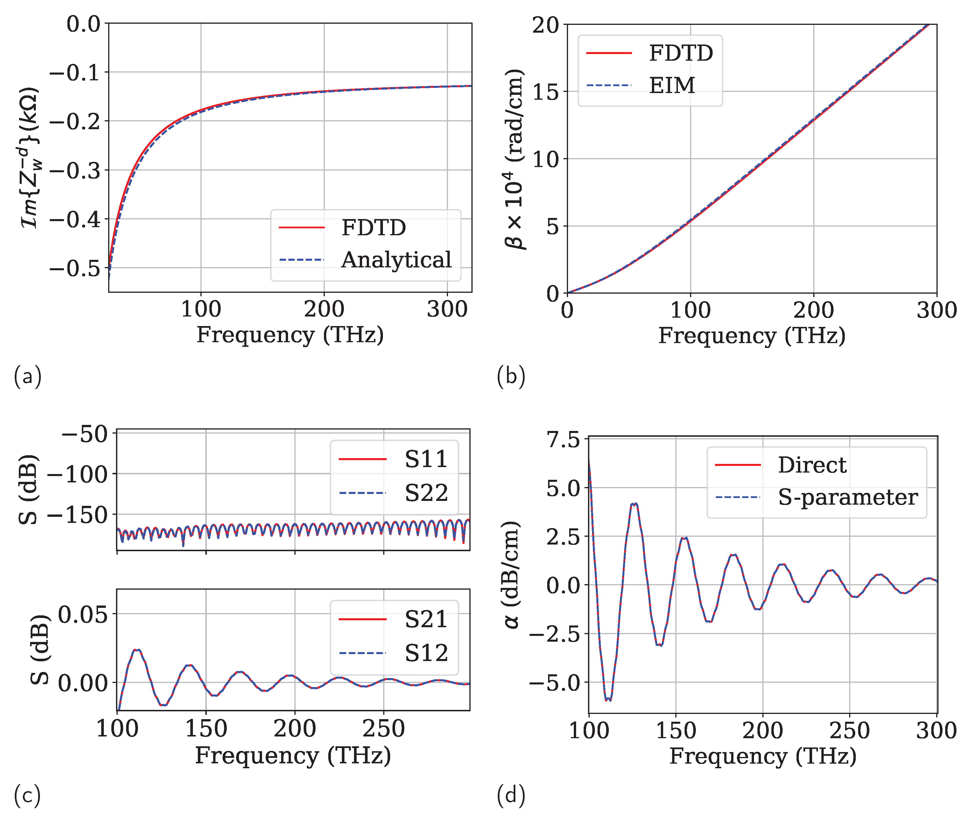
The wave impedance calculated from the FDTD model is shown in
Figure 5a. We can see that the impedance found from numerical experiment matches with the expected analytical value throughout this range of frequency samples. At
the difference between the FDTD and analytical values is approximately 1.5
, which translates to an error of less than
near the frequency of interest.
2.5.2. Propagation Constant
In the next validation method, we compare the propagation constant
obtained from FDTD against that obtained from the EIM in the frequency range of interest, at the same samples as the FDTD model output. We find
from FDTD by evaluating the imaginary component of (
9).
Since we are examining the phase angle of the voltage measurements, the division of
by
may be converted to a subtraction, resulting in (
22).
In FDTD, we compute the angle of the complex voltages over the entire frequency range on the smooth dielectric slab waveguide and unwrap the final angle array into full angle form (rather than principal angle form).
In
Figure 5b, the traces are nearly overlapped. The fundamental frequency is highlighted by the vertical dashed line, where the error between the EIM and the FDTD model is less than
. This data further validates the FDTD model, and confirms the formulation leading to (
22).
2.5.3. Scattering Matrix
In the last validation method, we utilize the properties of the S-parameters matrix described in
Section 2.3.1. As stated, the matrix should be symmetric and unitary for the smooth waveguide. We extract the S-parameters from the FDTD model using the method presented in
Section 2.3, and show these in
Figure 5c.
Two observations are noteworthy in the frequency range of interest: (1) the cross-terms (S12, S21) have a magnitude of near 0 dB, indicating that there is almost complete transmission of power from one end of the waveguide to the other, and the self-terms (S11, S22) are correspondingly very small compared to the cross-terms, with a peak value of less than dB; therefore, the matrix is nearly unitary as expected for a smooth lossless waveguide. (2) the S-parameter matrix is symmetrical, given the near perfect overlap of S11 with S22, and S12 with S21. These observations are noteworthy because they are the expected results for an ideal network, such as a smooth dielectric slab waveguide. Since the FDTD results align well with the expected behavior of a 2-port network, these results further validate the FDTD model.
We compare the
S-parameters method of
Section 2.3.1 and the
direct method of
Section 2.3.2 for calculating loss, as shown in
Figure 5d. Here, we observe an oscillatory behavior similar to that in the cross-terms of
Figure 5c. The oscillations hover around
dB/cm and decay with increasing frequency, while the expected per-unit-length attenuation for an ideal smooth waveguide is
dB/cm. Note that the loss from the S-parameters and from the direct method match very well, where the mean-squared error is on the order of
.
3. Results and Discussion
Unless stated otherwise, the data in this section are generated for waveguides with nm, , , THz, and nm.
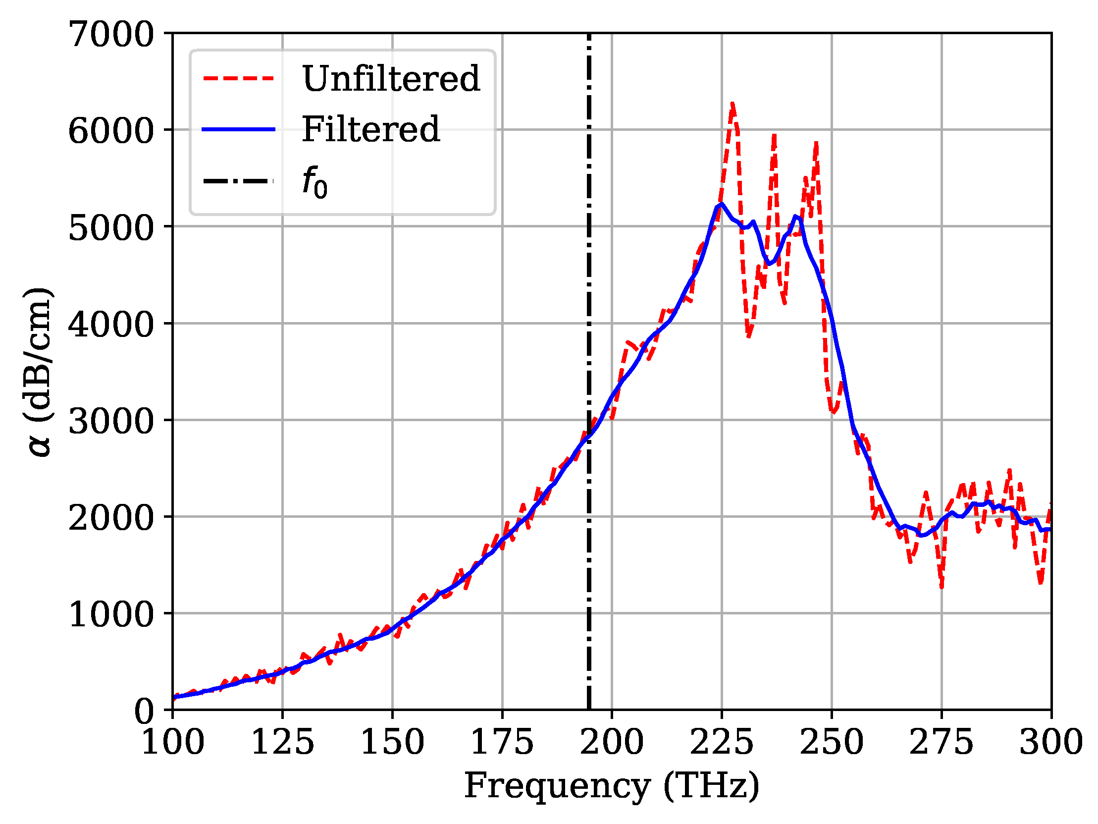
In
Figure 6, we show an example loss curve simulated in FDTD, to illustrate the need for filtering the FDTD output. As we can be seen in the figure, there is a nontrivial level of noise on the full range of
.
Applying the filter described in
Section 2.2.2 results in the
Filtered trace which considerably reduces the noise in the FDTD data. This is best exemplified by the
values for frequencies above 225 THz, where the noise is reduced by an order of magnitude. The
values from FDTD are subjected to this filtering technique prior to calculation of the percentage error between the FDTD and the analytical solution (
14).
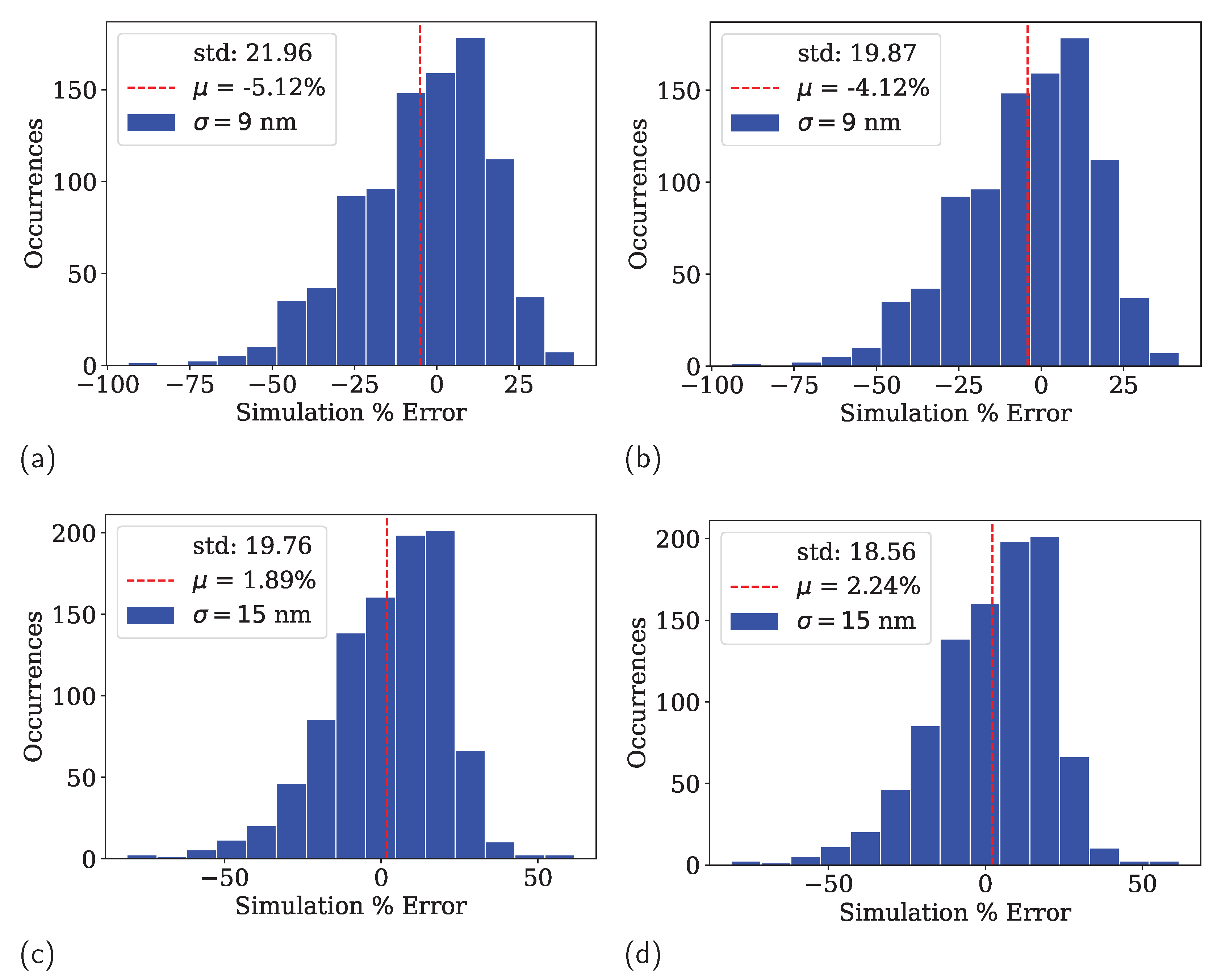
Figure 7 uses the data from tables I and II in [
7], respectively, to illustrate the distribution of percent error between FDTD and analytical calculations.
Figure 7a,b were generated with the standard deviation
nm. The correlation length
varies uniformly in the range 200 nm to 1000 nm. The figures show the distribution of percentage errors for all correlation lengths with the same standard deviation, where a total of 924 roughness profiles were simulated using the FDTD model. We use these data to illustrate the effect of filtering on simulation results. In
Figure 7a the mean error is
, whereas in
Figure 7b the error is reduced to
. Likewise, the standard deviation reduces from
to
.
A similar setup is used for
Figure 7c,d, where
nm and
is uniform in the range 200 nm to 1000 nm, with a total of 90 roughness profiles simulated with the FDTD model. In
Figure 7c the mean error is
, whereas in
Figure 7d the error is increased, to
. Like in the
plots, the standard deviation reduces, this time from
to
. From the numerical experiments conducted in FDTD on the relatively short-length slab waveguide, we have created the histogram of occurrences, which may be easily translated to a
probability mass distribution.
Some potential sources of error in
Figure 7 are listed below. (1) The parameters
, rather than
, are used in the analytical solution when calculating the percentage errors. (2) We use a relatively coarse spatial and temporal resolution in the FDTD model, while utilizing a finer resolution grid may decrease the percentage error range, it would increase computation time. (3) We use (
14) as the analytical model, which is based on the formulation originally proposed in [
5] that used various approximations and simplifications, such as a first-order Taylor series expansion to evaluate the E-field.
From each setup in
Figure 7 the maximum difference between filtered and unfiltered data is standard deviation from
Figure 7a,b which reduces by
, and each other relevant value changes by around
, with the mean percentage error in the
nm case actually increasing by
. This shows that the filtering step does not significantly impact the percentage error of the FDTD results from the analytical solution.
We define the
improvement metric as
where
,
,
and
are defined in
Section 2.2.2, and
is defined by (
14).
We use (
23) to compare the effect of filtering on the FDTD data. Using this metric, we consider any value greater than
to be an improvement, and
would indicate the filter has maximally improved the unfiltered signal. We consider
to be negligible change, i.e., filtering had little effect on unfiltered signal. For
nm, filtering improves the error in 487 instances out of 924, and that filtering has negligible effect for 62 instances. For
nm (
23) results in improvement for 462 instances out of 947, and negligible effect for 107 instances.
It is worth noting that the above technique involves filtering
after E- and H-fields have been computed in FDTD. The data show that filtering in this manner does not add significant value. Thus, we plan to investigate filtering techniques within FDTD
during the computation of E- and H-fields, as was demonstrated in [
28] for suppressing spurious noise waves due to sub-gridding.
3.1. Comparing Our Results to Previous Publications
We compare this work to previous theoretical and experimental works. Equation (
14) is based on the formulation provided in [
10], which in turn is based on both [
5,
8]. The primary difference between [
10] and this work is that here we introduce the normalization factor
. In [
10], the components for
are based on the more physically realistic form of E-field (
2) where
may be any real-valued scalar. The absence of the normalization factor (i.e., setting
) leaves a dependency on input power; however, the input power may be modified to fit the expected scattering loss value for any point, by setting (
24) equal to (
25) and solving for
, which will always result in (
29). In [
5], the original formulation for finding scattering loss was proposed, where the mathematical normalization of (
24) is used.
The follow-up work of [
8] proposed a formulation for scattering loss calculations by using normalized waveguide parameters, but as was noted in [
6], there appears to be an extra factor of 2 in the formulation used therein. We can see this numerically by comparing [
8] with this work, also in
Table 1, where the loss value is double what is calculated by (
14). We further see that an input power of
mW in the formulation found in [
10] is most similar to the normalized values found here, but other choices of input power (e.g.,
mW or
mW) could yield different values for loss as they may not eliminate dependence of
on input power.
The VCM was used in [
6] to verify the scattering loss calculations. Their work was done on several 3D waveguides, and these provide a similar analogue to the 2D structure simulated in this work.
Looking at the experimental side, in [
3] a physical 3D dielectric optical interconnect was tested for scattering loss. Their results show that the 2D planar model [
8] is generally an
overestimate of what can be expected from physical hardware, and the 3D simulations in [
6] are generally an
underestimate. Furthermore, in [
3], unit variance is used, making it unique compared to other experimental data and included in
Table 1. Other experiments conducted on physical hardware include those of [
1,
4], where a scattering loss magnitude of ≈35 dB/cm is reported. These experiments were conducted on 3D SOI optical interconnects consisting of Si core and SiO
2 cladding extending 1
m in each direction around the core, making them amenable to comparison with the 2D planar approximation. The loss value in [
1,
4] is approximately 36% of the loss value in (
14), and approximately 72% of the loss value in [
6].
3.2. Mode Normalization
Although allowing
to have dependency on waveguide’s structural attributes such as the surface roughness profile, material parameters, or even input wavelength is desirable, dependence on input power is not. In previous works [
5,
8], the E-field is mathematically normalized, such that
While the above normalization removes the dependence of
on the input power, it also forces
to satisfy a certain
mathematical requirement; however, if we evaluate (
24) by inserting the
physical field expression (
2) for the TE modes, we arrive at (
25) [
10].
Note that if (
24) is assumed to be true, then the field amplitude
would be forced to have the particular value
; however, this assumption may not hold true in the physical waveguide. To remedy the inconsistency, we start with [
5]
where the core and cladding refractive indices are tied to the guided power
and the radiated power
,
designates the ensemble average of
f [
10], and
[
5].
We use (15) from [
5] to simplify the numerator in (
26) and note that
cancels at this point, resulting in (
27).
We use the definition of
and
here to further simplify (
27); this results in (
28), where
in the numerator cancels and the
in the denominator is pulled into
.
We may further simplify (
28) for the zeroth-order mode by inserting the result from (
25) and the physical field amplitude expression of
in (
15), followed by canceling the resulting
term in the numerator and denominator.
Therefore, to remove dependence on input power uniformly for any initial input field amplitude, we propose to define
in (
14) as (
30), where
has the same dependence on input power as
.
Note that here, (
29) is the simplest form for even TE modes, using the physical considerations based on actual field values in the waveguide. In [
5], (
24), is assumed to be true prior to calculating
, forcing the denominator of (
28) to be
and limiting
to be single valued. The crucial difference in the proposed formulation here (based on inclusion of
in
) lies in the assumption that the E-field amplitude can be functionally
any value. We believe that the proposed normalization based on
offers a more physically consistent expression of
, and works more intuitively for correlation of numerical (or physical) experiments in FDTD (or in the lab) where the initial field amplitudes may be specified with regard to considerations independent of scattering loss.
4. Conclusions
Based on physical waveguide parameters, an explicit normalization factor (
30) for the scattering loss
(
14) was proposed. The equation was then used to compare the results across several previous publications, including both numerical and physical experiments, showing that the analytical equation is generally an overestimation of actual propagation loss in a physical waveguide. We used the proposed analytical equation to confirm the presence of an extra factor of 2 in [
8].
The proposed analytical formulation of scattering loss was verified, using an expedient FDTD scheme which included extraction of the attenuation coefficient and S-parameters. We validated the FDTD scheme by comparing numerical results against previously published analytical functions for the dielectric slab waveguide.
With the FDTD model verified, we demonstrated S-parameters extraction and attenuation coefficient calculation by applying the proposed methodology to a smooth dielectric slab waveguide. We then applied the methodology to compute the attenuation coefficient for a dielectric slab waveguide exhibiting random sidewall perturbations according to the exponential autocorrelation function. We proposed to use a filtering technique to reduce the signal-to-noise ratio of the final FDTD data in the frequency domain.
Along the way, we demonstrated the ability of the FDTD scheme to produce reasonably accurate results through tens of simulations for sidewall roughness profiles of varying correlation length at standard deviations of nm and nm. The FDTD results showed that the mean error for simulation is quite small, with an overall average error of only and for the attempted standard deviations, respectively.
The Python FDTD code (OIDT) [
13] used to generate much of the data in this paper was released as open-source software (under the GNU GPL v3.0 license [
15]) published on GitHub [
14], featuring multi-core support (for CPU) to compute the 2D TE
z fields of optical interconnects. Work is currently underway to develop efficient 2D transverse
magnetic (TM), and full 3D, FDTD models for further characterization of stochastic scattering loss due to sidewall roughness in nano-scale optical interconnects, consisting of single-line and multiple tightly-coupled lines, operating at 100 s of THz.


