

A Wireless Data Transfer by Using a Patch Antenna for Biomedical Applications

Abstract
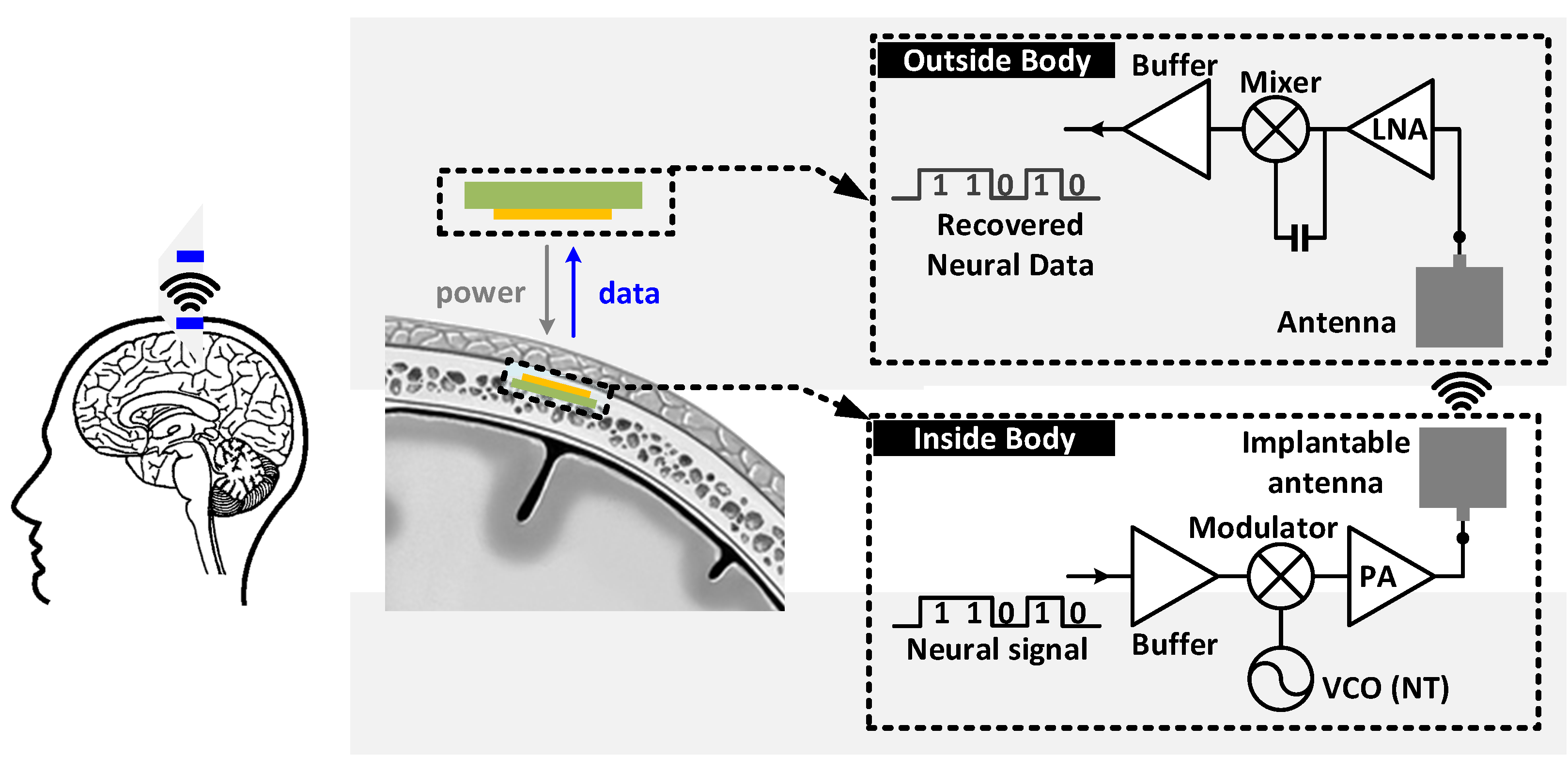
1. Introduction
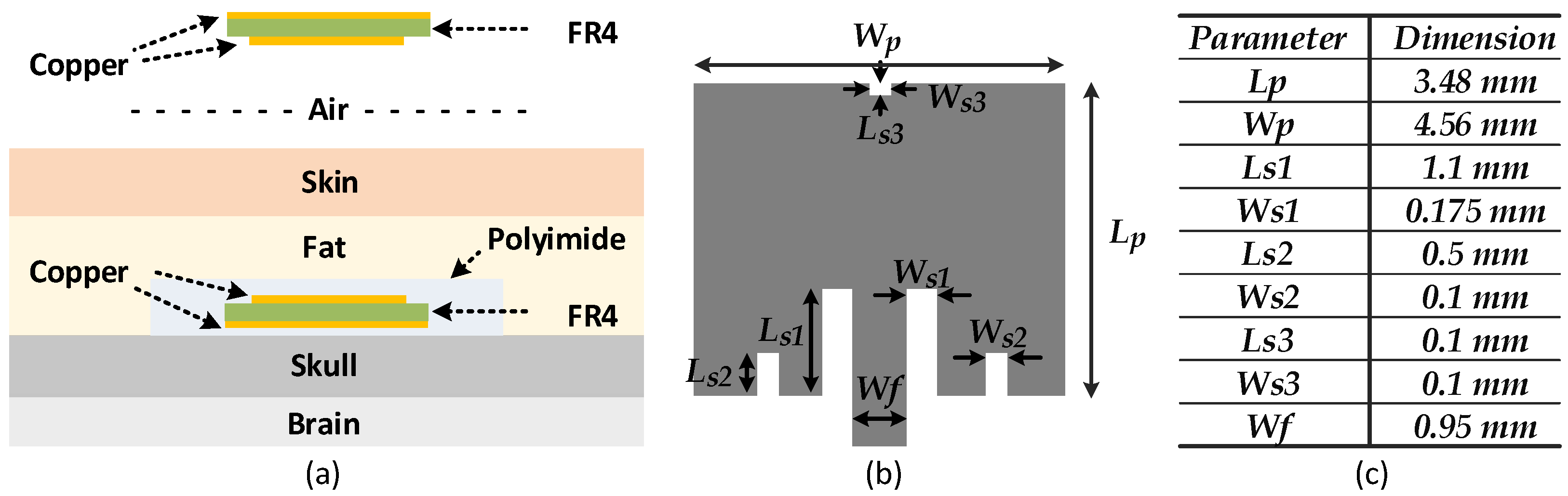
2. Biomedical Patch Antenna
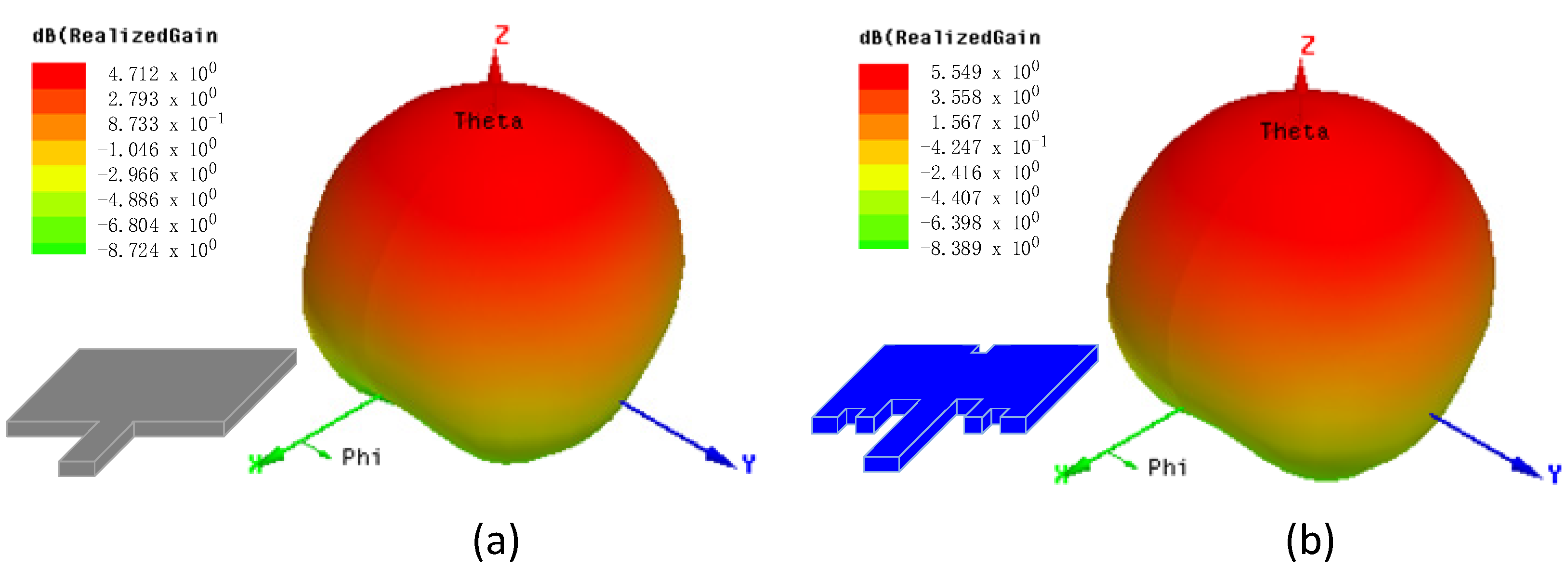
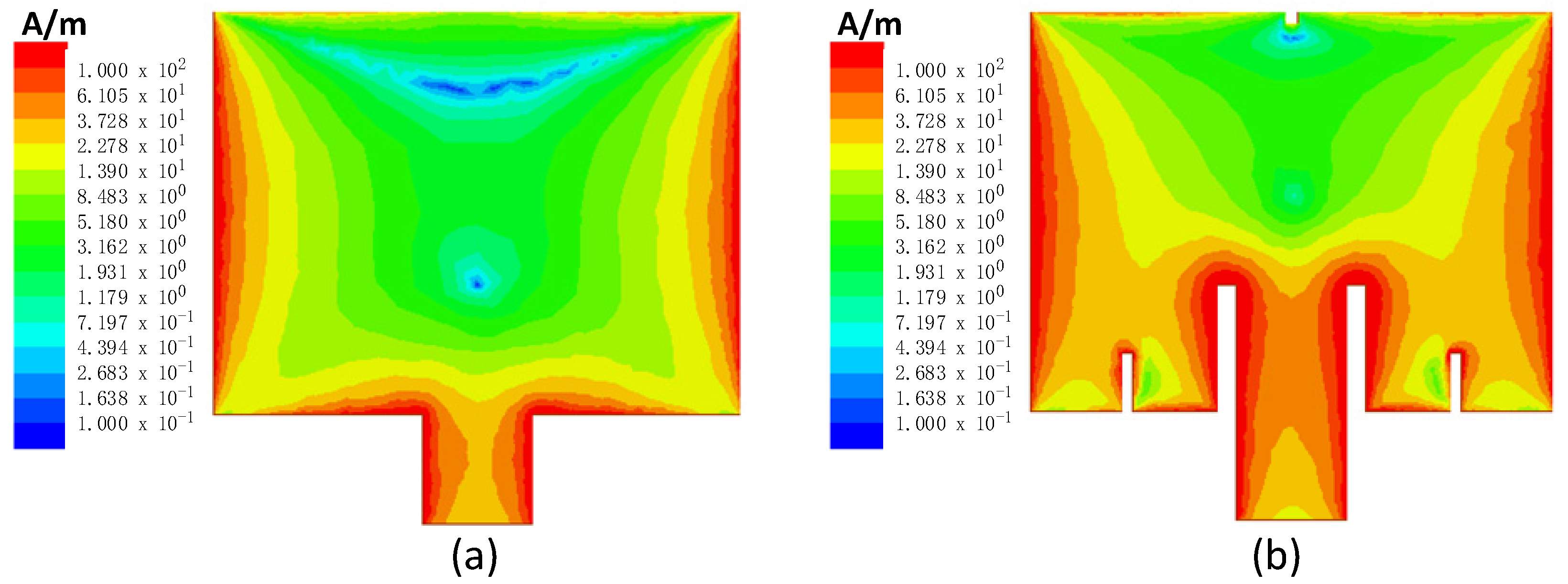
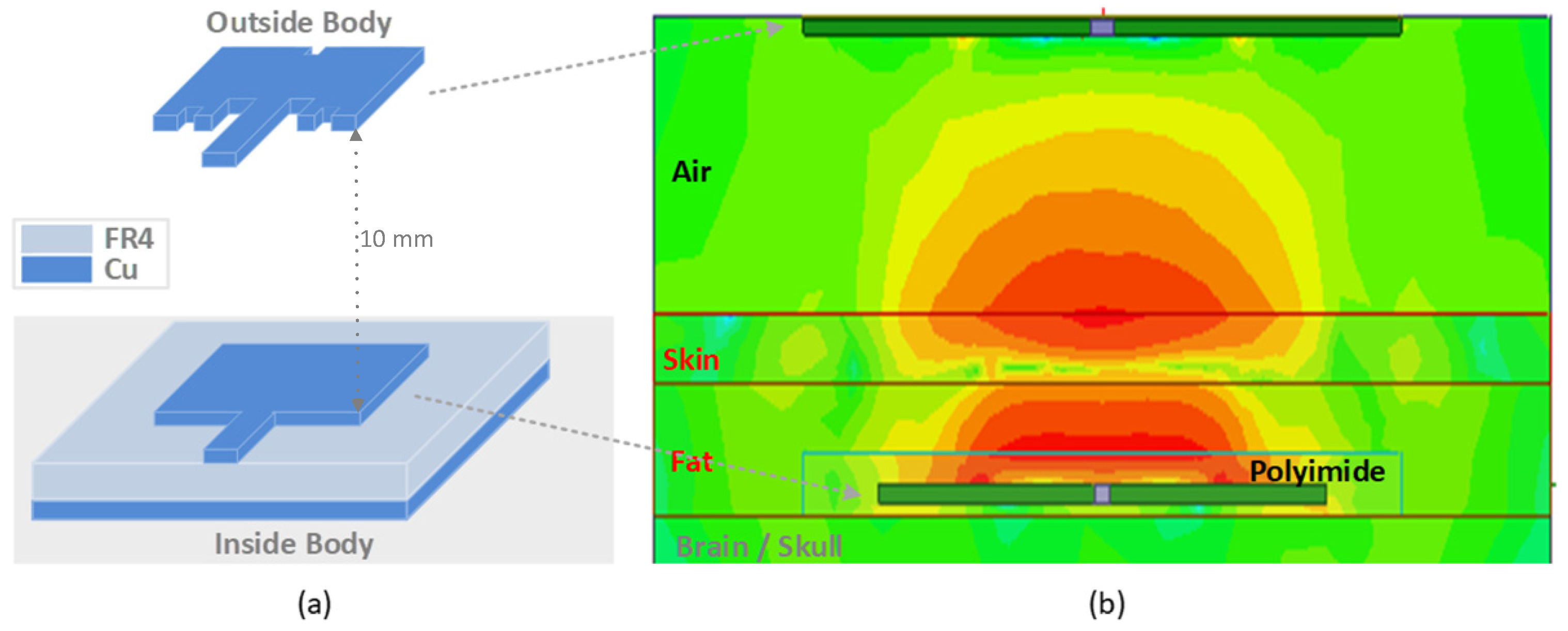
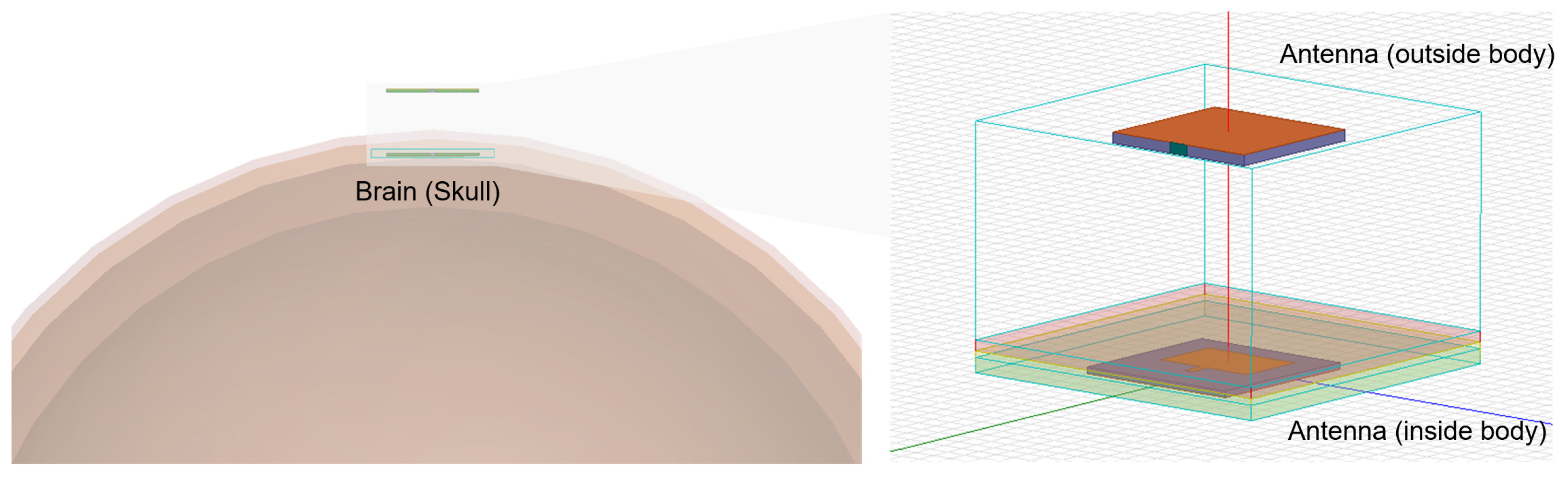
2.1. Proposed Implantable Notch Antenna Design
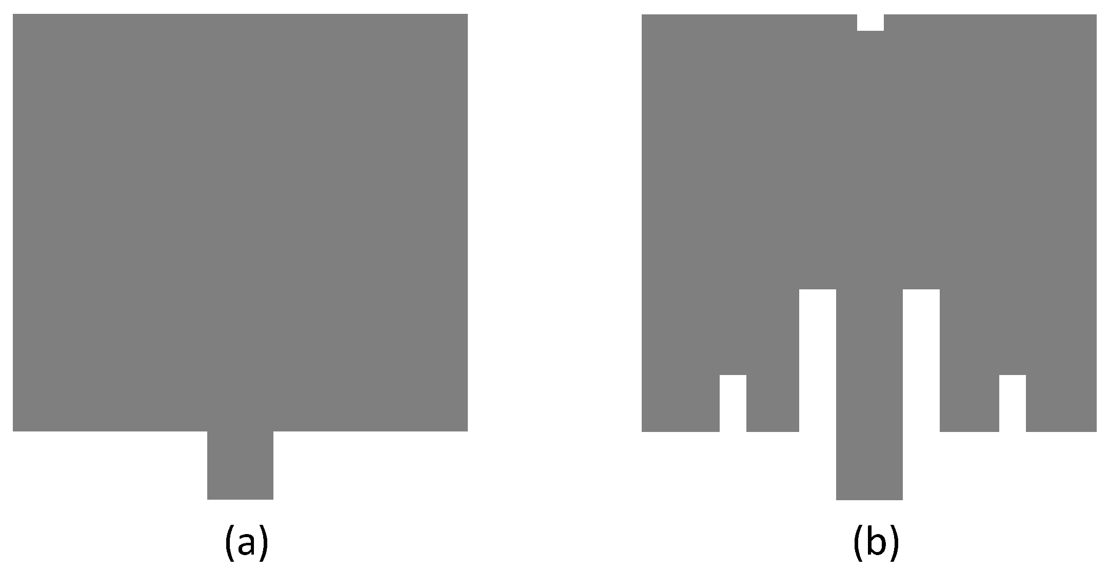
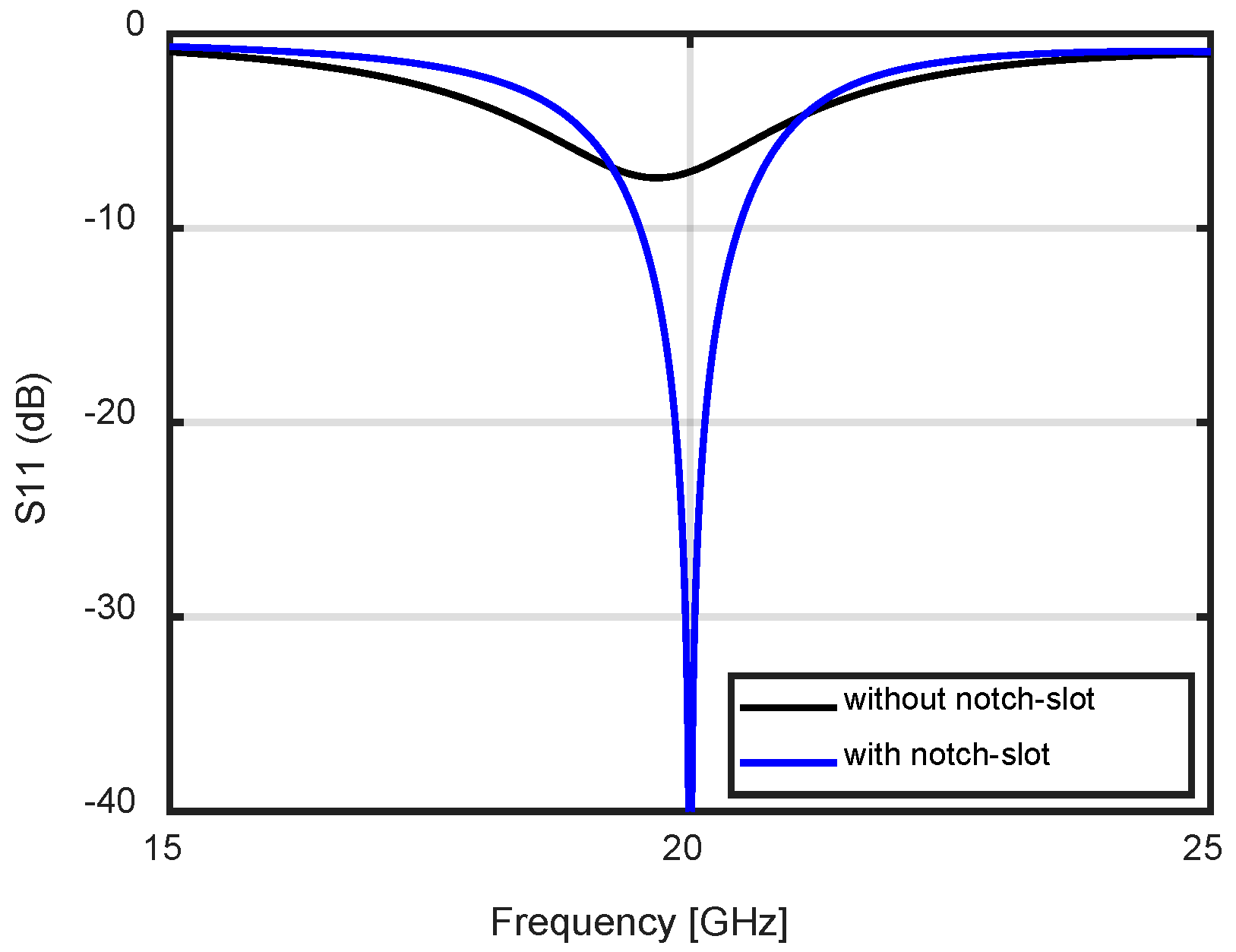
2.2. Patch Antenna Optimization
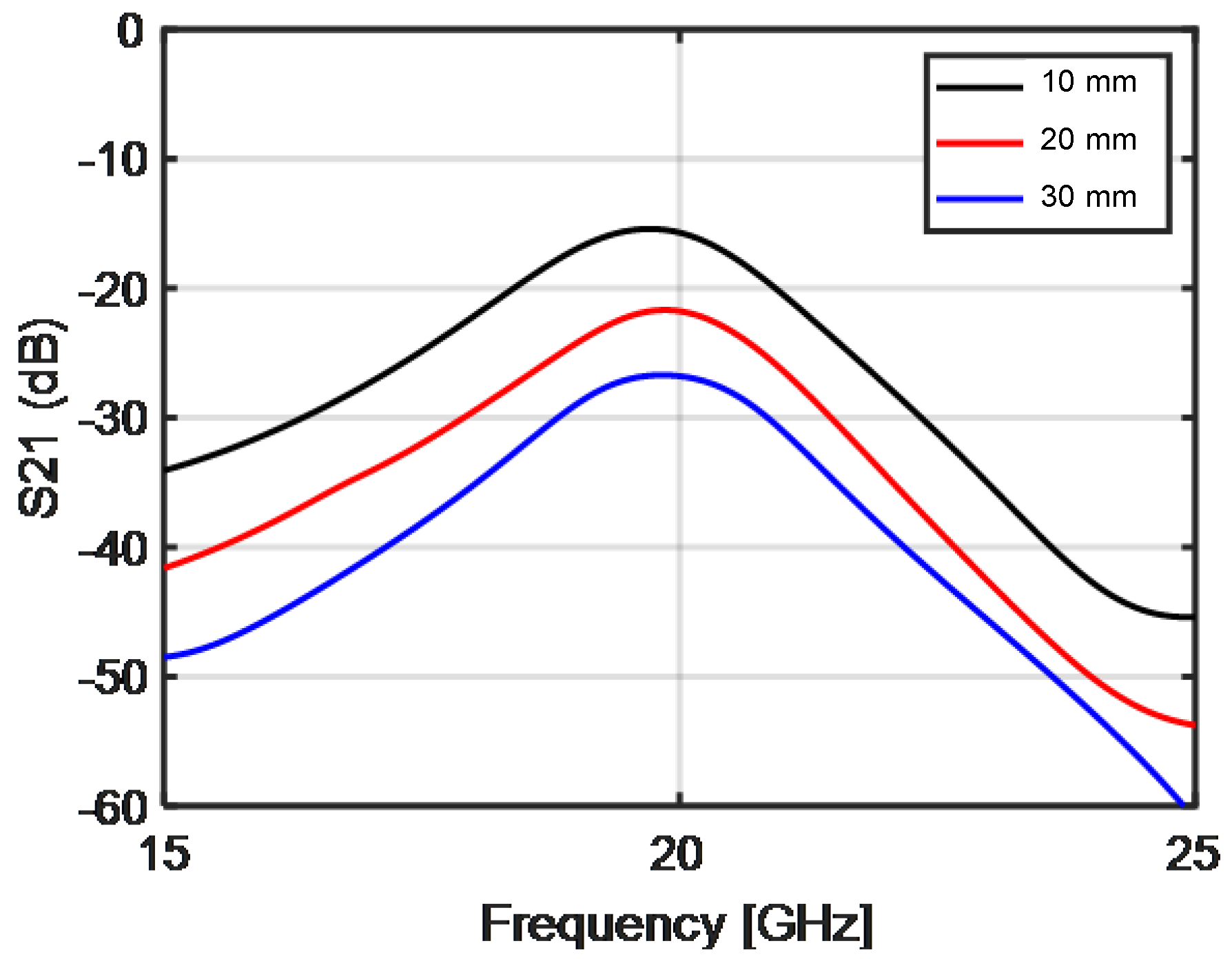
2.3. Performance of the Proposed Notch-Based Patch Antenna
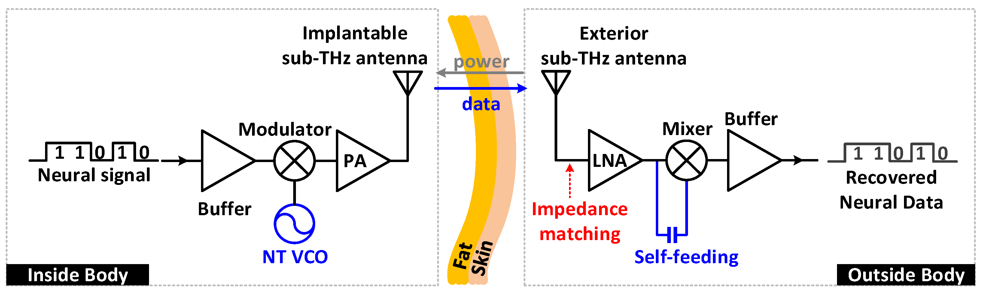
3. Wireless Data Transfer (WDT) System for Biomedical Applications
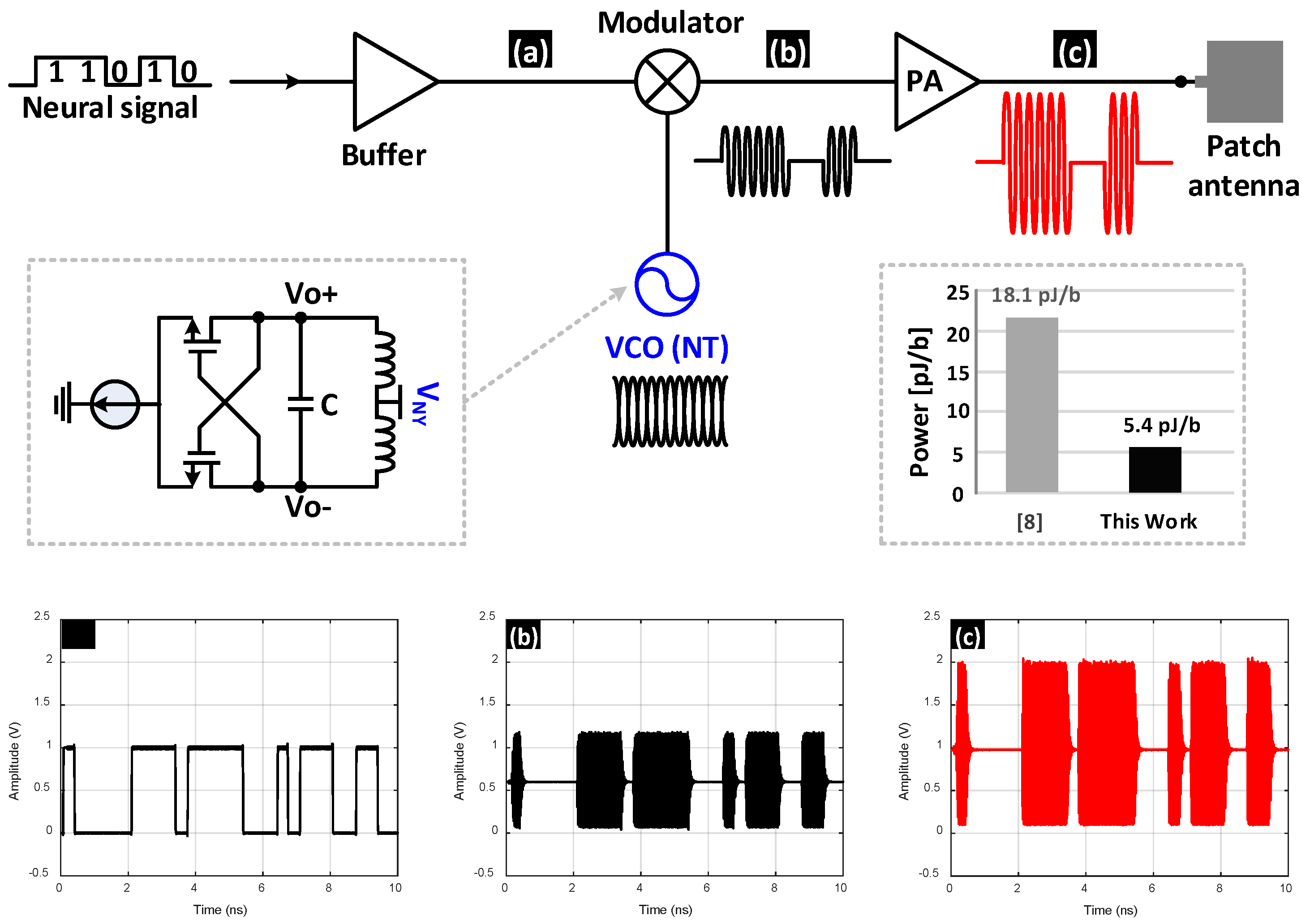
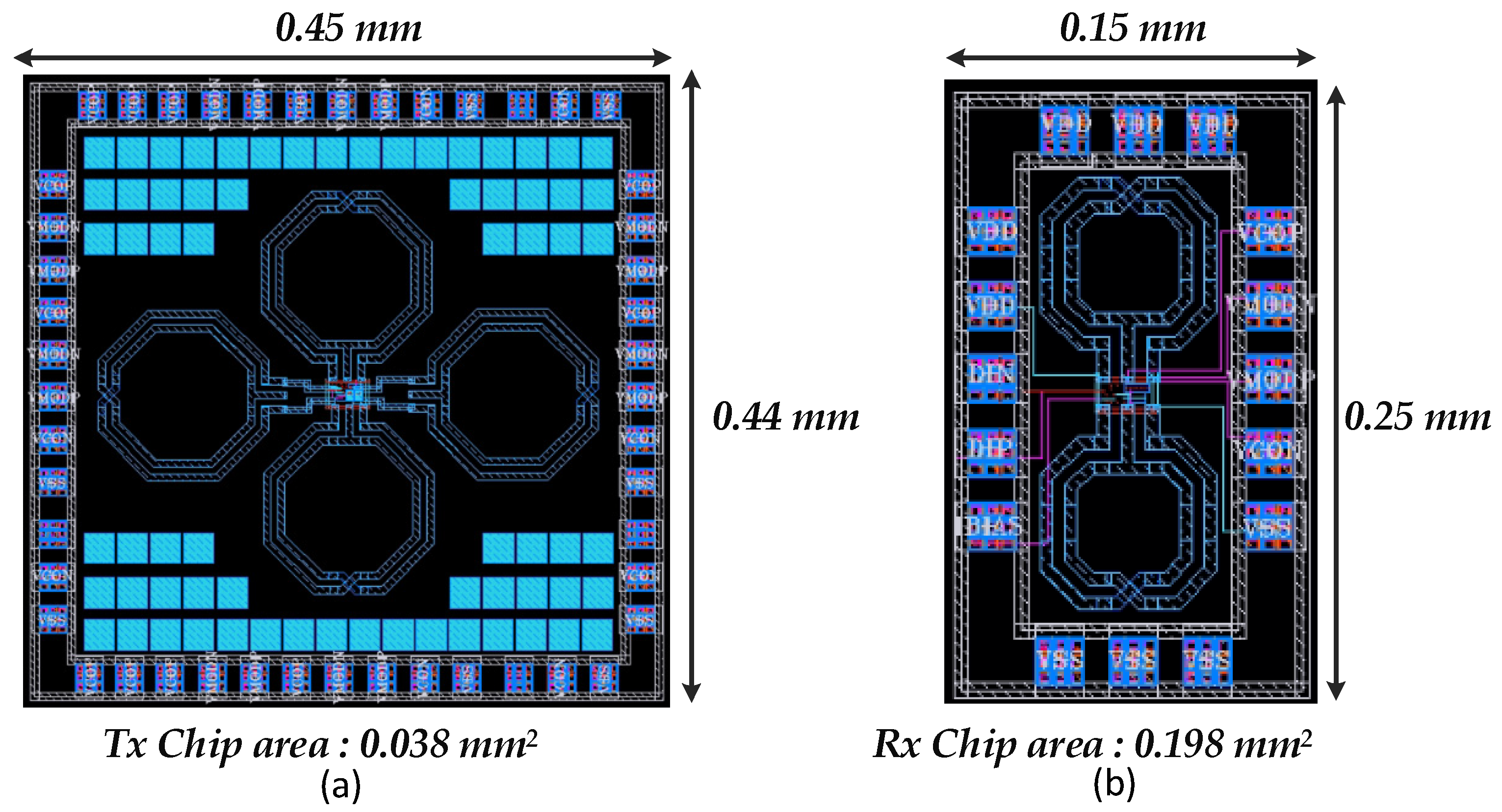
3.1. Proposed WDT Transmitter Design
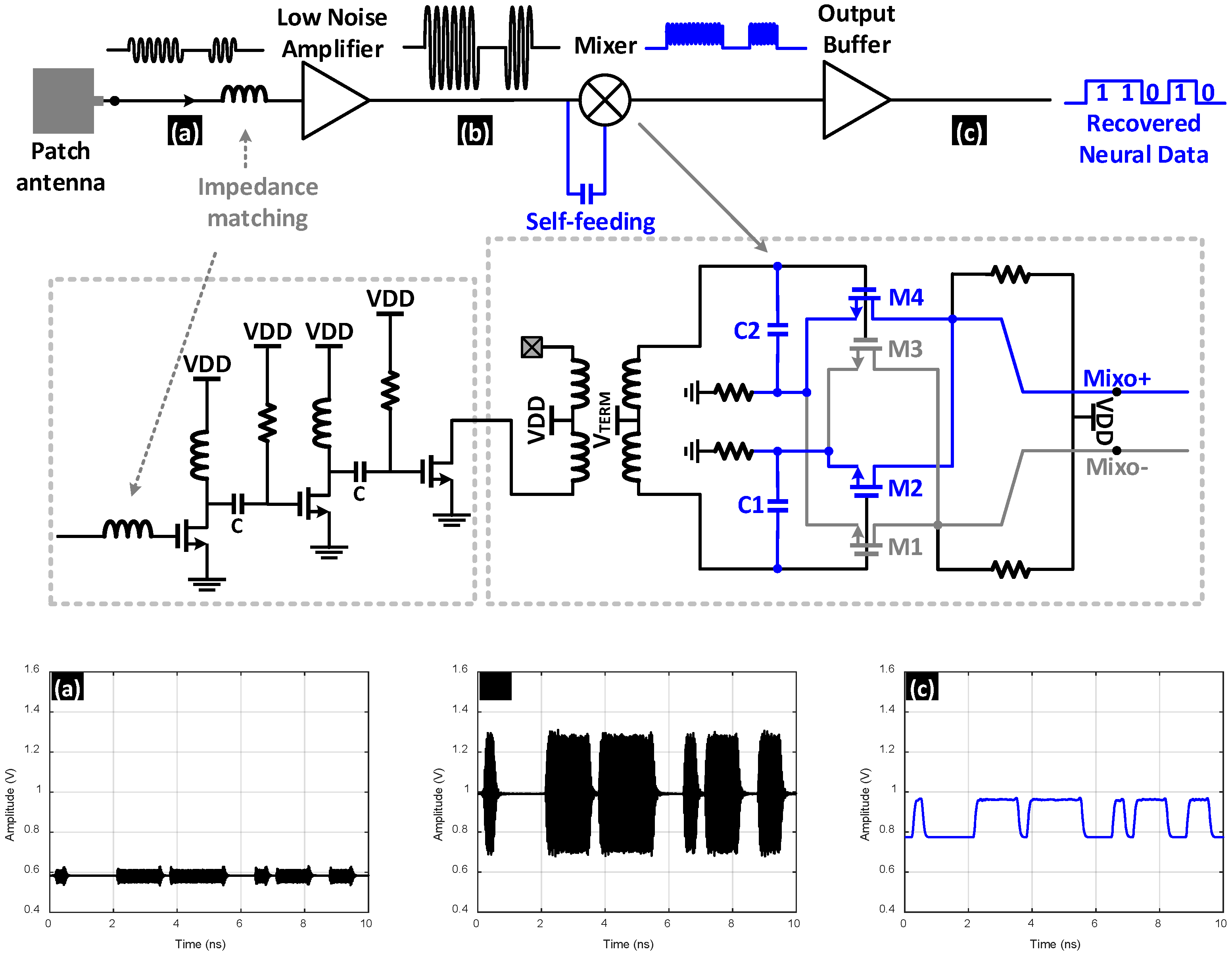
3.2. Proposed WDT Receiver Design
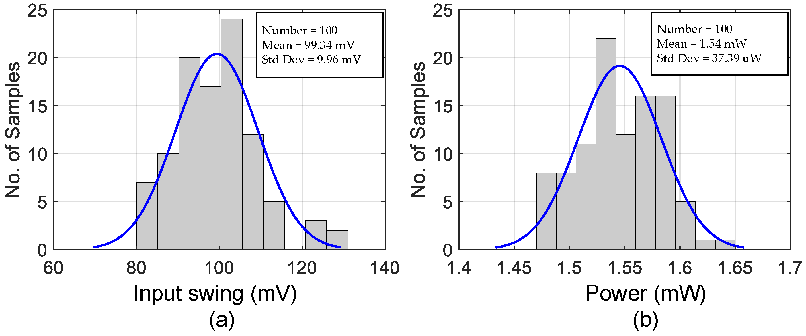
3.3. Performance Results of the Proposed WDT System
4. Conclusions
Funding
Institutional Review Board Statement
Informed Consent Statement
Conflicts of Interest
References
- Poon, C.C.Y.; Lo, B.P.L.; Yuce, M.R.; Alomainy, A.; Hao, Y. Body Sensor Networks: In the Era of Big Data and Beyond. IEEE Rev. Biomed. Eng. 2015, 8, 4–16. [Google Scholar] [CrossRef] [PubMed]
- Harrison, R.; Watkins, P.; Kier, R.; Lovejoy, R.; Black, D.; Normann, R.; Solzbacher, F. A Low-Power Integrated Circuit for a Wireless 100-Electrode Neural Recording System. Dig. Tech. Pap.—IEEE Int. Solid-State Circuits Conf. 2006, 42, 123–133. [Google Scholar] [CrossRef]
- Sodagar, A.M.; Perlin, G.E.; Yao, Y.; Najafi, K.; Wise, K.D. An Implantable 64-Channel Wireless Microsystem for Single-Unit Neural Recording. IEEE J. Solid-State Circuits 2009, 44, 2591–2604. [Google Scholar] [CrossRef]
- Chi, B.; Yao, J.; Han, S.; Xie, X.; Li, G.; Wang, Z. Low-Power Transceiver Analog Front-End Circuits for Bidirectional High Data Rate Wireless Telemetry in Medical Endoscopy Applications. IEEE Trans. Biomed. Eng. 2007, 54, 1291–1299. [Google Scholar] [CrossRef] [PubMed]
- Chaimanonart, N.; Young, D.J. A Wireless Batteryless in Vivo EKG and Body Temperature Sensing Microsystem with Adaptive RF Powering for Genetically Engineered Mice Monitoring. In Proceedings of the International Solid-State Sensors Actuators and Microsystems Conference, Denver, CO, USA, 21–25 June 2009; pp. 1473–1476. [Google Scholar] [CrossRef]
- Zhao, J.; Ghannam, R.; Htet, K.O.; Liu, Y.; Law, M.-K.; Roy, V.A.L.; Michel, B. Self-Powered Implantable Medical Devices Photovoltaic Energy Harvesting Review. Adv. Healthc. Mater. 2020, 9, 2000779. [Google Scholar] [CrossRef]
- Kiourti, A.; Nikita, K.S. A Review of Implantable Patch Antennas for Biomedical Telemetry: Challenges and Solutions. IEEE Antennas Propag. Mag. 2012, 54, 210–228. [Google Scholar] [CrossRef]
- Bhamra, H.; Huang, Y.W.; Yuan, Q.; Irazoqui, P. An Ultra-Low Power 2.4 GHz Transmitter for Energy Harvested Wireless Sensor Nodes and Biomedical Devices. IEEE Trans. Circuits Syst. II Express Briefs 2021, 68, 206–210. [Google Scholar] [CrossRef]
- Afroz, S.; Thomas, S.W.; Mumcu, G.; Saddow, S.E. Implantable SiC based RF antenna biosensor for continuous glucose mon-itoring. In Proceedings of the SENSORS, 2013 IEEE, Baltimore, MD, USA, 3–6 November 2013; pp. 1–4. [Google Scholar] [CrossRef]
- Sun, Y.; Greet, B.; Burkland, D.; John, M.; Razavi, M.; Babakhani, A. Wirelessly powered implantable pacemaker with on-chip antenna. In Proceedings of the 2017 IEEE MTT-S International Microwave Symposium (IMS), Honololu, HI, USA, 4–9 June 2017; pp. 1242–1244. [Google Scholar] [CrossRef]
- Chung, W.Y.; Le, G.T.; Tran, T.V.; Nguyen, N.H. Novel Proximal Fish Freshness Monitoring Using Batteryless Smart Sensor Tag. Sens. Actuators B Chem. 2017, 248, 910–916. [Google Scholar] [CrossRef]
- Gilmore, C.; Mojabi, P.; Zakaria, A.; Ostadrahimi, M.; Kaye, C.; Noghanian, S.; Shafai, L.; Pistorius, S.; Lovetri, J. A Wideband Microwave Tomography System with a Novel Frequency Selection Procedure. IEEE Trans. Biomed. Eng. 2010, 57, 894–904. [Google Scholar] [CrossRef]
- Mikhelson, I.V.; Bakhtiari, S.; Elmer, T.W.; Sahakian, A.V. Remote Sensing of Heart Rate and Patterns of Respiration on a Stationary Subject Using 94-GHz Millimeter-Wave Interferometry. IEEE Trans. Biomed. Eng. 2011, 58, 1671–1677. [Google Scholar] [CrossRef]
- Dilello, A.T.; Byun, G.S. An ultra-low power ASK modulator for back telemetry applications. In Proceedings of the IEEE WAMICON 2013, Orlando, FL, USA, 7–9 April 2013; pp. 1–4. [Google Scholar] [CrossRef]
- Kiourti, A.; Nikita, K.S. Miniature Scalp-Implantable Antennas for Telemetry in the MICS and ISM Bands: Design, Safety Considerations and Link Budget Analysis. IEEE Trans. Antennas Propag. 2012, 60, 3568–3575. [Google Scholar] [CrossRef]
- Kim, J.; Rahmat-Samii, Y. Implanted Antennas inside a Human Body: Simulations, Designs, and Characterizations. IEEE Trans. Microw. Theory Tech. 2004, 52, 1934–1943. [Google Scholar] [CrossRef]
- Song, L.; Rahmat-Samii, Y. An End-to-End Implanted Brain-Machine Interface Antenna System Performance Characterizations and Development. IEEE Trans. Antennas Propag. 2017, 65, 3399–3408. [Google Scholar] [CrossRef]
- Naqvi, S.A.R.; Mobashsher, A.T.; Mohammed, B.; Foong, D.; Abbosh, A. Benign and Malignant Skin Lesions: Dielectric Characterization, Modelling and Analysis in Frequency Band 1 to 14 GHz. IEEE Trans. Biomed. Eng. 2022, 1–12. [Google Scholar] [CrossRef] [PubMed]
- Elshaekh, D.; Kayed, S.; Shawkey, H. Single-Chip Two Antennas for Mm-Wave Self-Powering and Implantable Biomedical Devices. Appl. Comput. Electromagn. Soc. J. 2021, 36, 885–893. [Google Scholar] [CrossRef]
- Zhang, Y.; Liu, C.; Liu, X.; Zhang, K.; Yang, X. A Wideband Circularly Polarized Implantable Antenna for 915 MHz ISM-Band Biotelemetry Devices. IEEE Antennas Wirel. Propag. Lett. 2018, 17, 1473–1477. [Google Scholar] [CrossRef]
- Faisal, F.; Zada, M.; Ejaz, A.; Amin, Y.; Ullah, S.; Yoo, H. A Miniaturized Dual-Band Implantable Antenna System for Medical Applications. IEEE Trans. Antennas Propag. 2020, 68, 1161–1165. [Google Scholar] [CrossRef]
- Xia, Z.; Li, H.; Lee, Z.; Xiao, S.; Shao, W.; Ding, X.; Yang, X. A Wideband Circularly Polarized Implantable Patch Antenna for ISM Band Biomedical Applications. IEEE Trans. Antennas Propag. 2020, 68, 2399–2404. [Google Scholar] [CrossRef]
- Green, R.B.; Hays, M.; Mangino, M.; Topsakal, E. An Anatomical Model for the Simulation and Development of Subcutaneous Implantable Wireless Devices. IEEE Trans. Antennas Propag. 2020, 68, 7170–7178. [Google Scholar] [CrossRef]
- Zada, M.; Shah, I.A.; Basir, A.; Yoo, H. Ultra-Compact Implantable Antenna with Enhanced Performance for Leadless Cardiac Pacemaker System. IEEE Trans. Antennas Propag. 2021, 69, 1152–1157. [Google Scholar] [CrossRef]
- Blauert, J.; Member, S.; Kang, Y.; Kiourti, A. In Vivo Testing of a Miniature 2.4/4.8 GHz Implantable Antenna in Postmortem Human Subject. IEEE Antennas Wirel. Propag. Lett. 2018, 17, 2334–2338. [Google Scholar] [CrossRef]
- Byun, G.S.; Kim, Y.; Kim, J.; Tam, S.W.; Chang, M.C.F. An Energy-Efficient and High-Speed Mobile Memory I/O Interface Using Simultaneous Bi-Directional Dual (Base+RF)-Band Signaling. IEEE J. Solid-State Circuits 2012, 47, 117–130. [Google Scholar] [CrossRef]
- Gao, Y.; Zheng, Y.; Diao, S.; Da Toh, W.; Ang, C.W.; Je, M.; Heng, C.H. Low-Power Ultrawideband Wireless Telemetry Transceiver for Medical Sensor Applications. IEEE Trans. Biomed. Eng. 2011, 58, 768–772. [Google Scholar] [CrossRef] [PubMed]
- Lee, S.Y.; Cheng, P.H.; Tsou, C.F.; Lin, C.C.; Shieh, G.S. A 2.4 GHz ISM Band OOK Transceiver with High Energy Efficiency for Biomedical Implantable Applications. IEEE Trans. Biomed. Circuits Syst. 2020, 14, 113–124. [Google Scholar] [CrossRef] [PubMed]
- Gabriel, C.; Gabriel, S.; Corthout, E. The Dielectric Properties of Biological Tissues: I. Literature Survey. Phys. Med. Biol. 1996, 41, 2231–2249. [Google Scholar] [CrossRef]
- Ture, K.; Devos, A.; Maloberti, F.; Dehollain, C. Area and Power Efficient Ultra-Wideband Transmitter Based on Active Inductor. IEEE Trans. Circuits Syst. II Express Briefs 2018, 65, 1325–1329. [Google Scholar] [CrossRef]
- Gusland, D.; Christiansen, J.M.; Torvik, B.; Gurbuz, S.Z.; Fioranelli, F.; Ritchie, M. Open Radar Initiative: Large Scale Dataset for Benchmarking of Micro-Doppler Recognition Algorithms. In Proceedings of the 2021 IEEE Radar Conference (RadarConf21), Atlanta, GA, USA, 7–14 May 2021. [Google Scholar]
- Lin, Y.; Park, S.; Chen, X.; Wentzloff, D.; Yoon, E. 4.32-PJ/b, Overlap-Free, Feedforward Edge-Combiner-Based Ultra-Wideband Transmitter for High-Channel-Count Neural Recording. IEEE Microw. Wirel. Components Lett. 2018, 28, 52–54. [Google Scholar] [CrossRef]
- Zhang, Z.; Li, Y.; Mouthaan, K.; Lian, Y. A Miniature Mode Reconfigurable Inductorless IR-UWB Transmitter-Receiver for Wireless Short-Range Communication and Vital-Sign Sensing. IEEE J. Emerg. Sel. Top. Circuits Syst. 2018, 8, 294–305. [Google Scholar] [CrossRef]
- Byeon, C.W.; Eun, K.C.; Park, C. A 2.65-PJ Bit 12.5-Gbs 60-GHz OOK CMOS Transmitter and Receiver for Proximity Communications. Medium 2020, 68, 1–6. [Google Scholar] [CrossRef]
- De Streel, G.; Stas, F.; Gurne, T.; Durant, F.; Frenkel, C.; Cathelin, A.; Bol, D. SleepTalker: A ULV 802.15.4a IR-UWB Transmitter SoC in 28-Nm FDSOI Achieving 14 PJ/b at 27 Mb/s with Channel Selection Based on Adaptive FBB and Digitally Programmable Pulse Shaping. IEEE J. Solid-State Circuits 2017, 52, 1163–1177. [Google Scholar] [CrossRef]


| Layer | Skin | Fat | Skull | Brain |
|---|---|---|---|---|
| 33.04 | 9.35 | 8.12 | 31.8 | |
| Δ (S/m) | 6.27 | 1.32 | 2.14 | 10 |
| Thickness (mm) | 0.5 | 1 | 8 | 4 |
| Parameter | AWPL 2018 [20] | TAP 2019 [21] | TAP 2020 [22] | TAP 2020 [23] | TAP 2021 [24] | AWPL 2018 [25] | ACS 2021 [19] | This Work |
|---|---|---|---|---|---|---|---|---|
| Frequency (GHz) | 0.9 | 0.9 | 2.4 | 2.4 | 2.4 | 4.8 | 22 | 20 |
| Dimension (mm2) | 66.5 | 49 | 96 | 272.2 | 12 | 53.2 | 0.55 | 17 |
| S11 (dB) | −30 | −18 | −26 | −22 | NA | −10 | −19 | −16 |
| S11 ≤ −10dB (MHz) | 112 | 107.5 | 540 | 140 | 525 | 115 | NA | 940 |
| Gain (dBi) | −32.8 | −27.65 | −33 | −11.3 | −25.9 | −12 | −20 | −0.07 |
| Parameter | TICAS-II 2018 [30] | TICAS-I 2018 [31] | MWCL 2018 [32] | JETCAS 2018 [33] | TMTT 2020 [34] | JSSC 2017 [35] | This Work |
|---|---|---|---|---|---|---|---|
| CMOS technology | 180 nm | 130 nm | 65 nm | 65 nm | 65 nm | 28 nm | 28 nm |
| Modulation | OOK | OOK | OOK | OOK | OOK | OOK | OOK |
| Freq. band (GHz) | 6 | 4.5 | 4.1 | 8 | 60 | 4.5 | 20 |
| Data rate (Mb/s) | 200 | 1000 | 200 | 10 | 12.5 | 27.24 | 1800 |
| Power supply (V) | 1.8 | 1.2 | 1 | 1.2 | NA | 0.55 | 1 |
| Energy (pJ/b) | 20 | 5 | 4.3 | 21.6 | 2.65 | 14 | 5.4 |
Publisher’s Note: MDPI stays neutral with regard to jurisdictional claims in published maps and institutional affiliations. |
© 2022 by the author. Licensee MDPI, Basel, Switzerland. This article is an open access article distributed under the terms and conditions of the Creative Commons Attribution (CC BY) license (https://creativecommons.org/licenses/by/4.0/).
Share and Cite
Byun, G.-S. A Wireless Data Transfer by Using a Patch Antenna for Biomedical Applications. Electronics 2022, 11, 4197. https://doi.org/10.3390/electronics11244197
Byun G-S. A Wireless Data Transfer by Using a Patch Antenna for Biomedical Applications. Electronics. 2022; 11(24):4197. https://doi.org/10.3390/electronics11244197
Chicago/Turabian StyleByun, Gyung-Su. 2022. "A Wireless Data Transfer by Using a Patch Antenna for Biomedical Applications" Electronics 11, no. 24: 4197. https://doi.org/10.3390/electronics11244197
APA StyleByun, G.-S. (2022). A Wireless Data Transfer by Using a Patch Antenna for Biomedical Applications. Electronics, 11(24), 4197. https://doi.org/10.3390/electronics11244197