Article

A 1.25 MHz, 108 dB Chopped Sampling-Mixer-Based Impedance Spectroscopy SoC in 0.18-μm CMOS

Department of Electrical and Electronics Engineering, Konkuk University, Seoul 05029, Republic of Korea
*
Author to whom correspondence should be addressed.
Electronics 2022, 11(24), 4130; https://doi.org/10.3390/electronics11244130
Submission received: 15 November 2022 / Revised: 7 December 2022 / Accepted: 9 December 2022 / Published: 11 December 2022
(This article belongs to the Special Issue Mixed Signal Circuit Design)

Abstract

:
This paper presents an electrochemical impedance spectroscopy (EIS) system-on-chip in 0.18- μ m CMOS, achieving a wide scan frequency range of 1.25 MHz. An on-chip direct digital frequency synthesizer generates a digital sine wave as well as in-phase and quadrature-phase clocks that are synchronized to the sinewave. A chopped sampling mixer realizes lock-in detection without requiring quadrature sinewaves while suppressing low-frequency noise and offset. The receive utilizes a 12-bit pipelined SAR ADC operating in 5 MS/s in combination with a digital averaging filter to maximize the dynamic range. The measured performance shows that the prototype EIS chip achieves the highest frequency scan range with a comparable dynamic range of 108 dB and power consumption of 14 mW when compared with the previous state-of-the-art prototypes.

1. Introduction

Electrochemical impedance spectroscopy (EIS) is used in various sensor applications that require impedance measurement of a specific target [1,2,3,4,5,6,7]. Notable examples include gas concentration measurement [1], battery condition measurement, [2] human body composition analysis [3], impedance cardiography [4], and lung ventilation monitor [5]. It is also applied to systems that detect molecular substances ranging from intracellular action potential [6], DNA [7], and RNA [8] detection. In these applications, it is commonly required to accurately measure the impedance over a wide frequency range. For instance, DNA and RNA are typically measured between 100 Hz and 10 kHz, whereas some DNA detections are measured up to MHz frequencies [9]. Therefore, it would be ideal if the EIS system could cover a wide frequency range with a fine frequency resolution.
Traditionally, the EIS system has been implemented using a lock-in amplifier followed by a low-pass filter and an A/D converter [10,11]. However, it is challenging to design a general-purpose EIS system covering a wide frequency range. Specifically, a lock-in-based EIS system requires a quadrature analog multiplier with a variable clock frequency generator. Hence, this system must deal with various analog design issues, such as mismatches between in-phase and quadrature-phase (I/Q) signals. A full-digital lock-in system that did not suffer from the quadrature mismatch was demonstrated in [12], but it requires complex digital signal processing that includes high-speed digital multiplication, not to mention the necessity of a high-resolution and high-performance A/D converter (ADC). A recently presented FFT-based impedance analysis has the advantage of calculating impedance at multiple frequencies with a single A/D conversion followed by an FFT analysis, but this system requires a very high-resolution ADC such as 16-bit or 24-bit [1], which is challenging to design, especially when the required ADC clock frequency is over MHz ranges.
In this paper, we present a wide-frequency EIS system-on-chip (SoC) in 0.18- μ m CMOS by utilizing the concept of a sampling mixer. The proposed EIS architecture offers a new way of measuring the impedance over a wide frequency range without using an analog multiplier or a complex FFT engine. Our prototype EIS system is designed as a system-on-chip, which includes a 10-bit direct digital frequency synthesizer (DDFS) with an embedded I/Q generator, a quadrature chopped sampling-mixer front-end, and a 5 MS/s, 2-stage, 12-bit pipelined successive approximation-register ADC for impedance detection. The measured performance confirms the validity of the operation by demonstrating a dynamic range of 108 dB with up to 1.25 MHz impedance frequency scan range. The measured performance is comparable to a state-of-the-art EIS system in terms of frequency and dynamic ranges.
The paper is organized as follows. Section 2 begins with a review of the lock-in impedance detection, followed by introducing a concept of the sampling-mixer-based impedance detection technique. Section 3 shows the architecture of our EIS SoC and describes details of the key circuits that include both the transmitter and the receiver. Section 4 presents the experimental results with a brief discussion. Section 5 concludes the paper.

2. Sampling-Mixer-Based Impedance Spectroscopy

This section begins with a review of lock-in detection, which is the underlying theory of impedance spectroscopy, followed by the concept of the proposed sampling-mixer-based impedance detection technique.

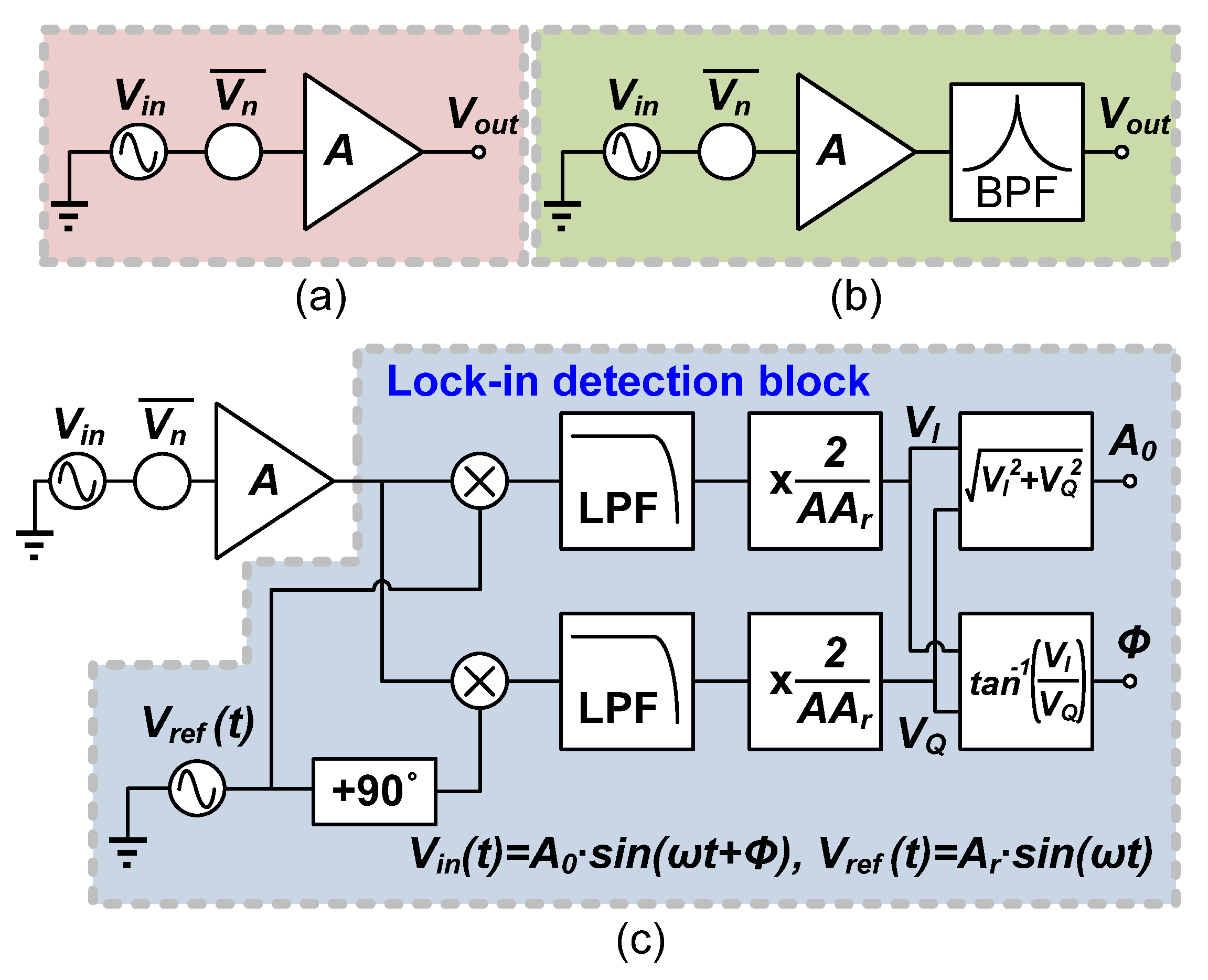
2.1. Review of Lock-In Detection Theory

Measuring the complex impedance of a target can be accomplished by measuring the magnitude and phase response of the target. Therefore, in many sensor applications, the transmitter generates a sinewave that passes through the target to be sensed, and the receiver measures the response, which is then post-processed to calculate the impedance. By iterating this process over a large number of discrete frequencies, one can find the overall impedance characteristic versus frequency, which is often called electrochemical impedance spectroscopy (EIS). Lock-in detection is the most traditional and popular technique in EIS when detecting a very small signal with a magnitude of nV-level under the presence of broadband noise.
To explain the difficulty, consider the cases shown in Figure 1. It is assumed that the amplifier has a DC gain of 1000 [V/V] with a pole frequency of 100 kHz and an input-referred noise level is V n ¯ = 5 n V / H z . It is also assumed that the input signal has an amplitude of 10 nV with a frequency of 10 kHz.
Figure 1a illustrates the case when no filtering is used. In this case, the total integrated RMS noise voltage ( V n , o u t ¯ ) at the output is calculated as
V n , o u t ¯ = 5 n V H z × 1000 × π 2 × 100 k H z   = 2   m V r m s   ,
Because the output signal amplitude after the amplifier is only 10 μ V , the output SNR is −49 dB, and it is impossible to detect such a signal. Figure 1b illustrates the case that utilizes a sharp band-pass filter with a quality factor (Q) of 100. In this case, the integrated noise power after the filtering can be calculated as
V n , o u t ¯ = 5 n V H z × 1000 × 100 H z = 50 μ V r m s   ,
leading to an output SNR of −17 dB, which is still not acceptable. To alleviate this difficulty, the lock-in amplifier shown in Figure 1c down-converts the signal by quadrature multiplication. Since the signal is located at DC after the down-conversion, a low-pass filter with an extremely low bandwidth can be used to filter out the noise. For instance, if the filter bandwidth is 0.01 Hz, V n , o u t ¯ is given by
V n , o u t ¯ = 5 n V H z × 1000 × 0.01 H z = 500 n V r m s   ,  
which results in acceptable SNR of 23 dB (Mathematical derivation of the lock-in detection is included in the Appendix A).

2.2. Sampling-Mixer-Based Impedance Measurement

A key challenge in using lock-in detection for an integrated EIS SoC design is the necessity of a high-linearity analog quadrature multiplier. Moreover, generating a quadrature sinewave over a wide frequency range is not trivial. In this work, we propose to use an alternative technique based on a sampling mixer [13], which is used in wireless RF receiver designs. The central idea is that when the received signal after the target is sampled by quadrature clocks having the exact same frequency as the signal, both the magnitude and phase response of the target can be recovered. Specifically, suppose that the received signals after the quadrature sampling are given by
V I ,   R X = A 0 sin ( 2 π f s t 1 + ϕ ) ,
V Q ,   R X = A 0 sin ( 2 π f s ( t 1 + 1 4 1 f s ) + ϕ ) = A 0 cos ( 2 π f s t 1 + ϕ ) ,
where A 0 is the amplitude of the received sinewave that reflects the magnitude of the impedance. From these two values, one can easily calculate the magnitude as
A 0 = V I , R X 2 + V Q , R X 2 ,
ϕ = tan 1 ( V I , R X V Q , R X )   .
Note the sampling-mixer-based impedance measurement does not require a quadrature sinewave, which is difficult to realize in CMOS circuits. Instead, it requires a quadrature clock and a sampler that are more compatible with CMOS design. There are several key circuit blocks when one wants to implement the sampling-mixed-based impedance measurement. They include: (1) A programmable sinewave and quadrature clock generator, (2) A sampling mixer front-end, and (3) A high-resolution A/D converter. In the following section, we will describe the architecture of our EIS SoC and present details of the circuit implementation.

3. EIS Architecture and Implementation

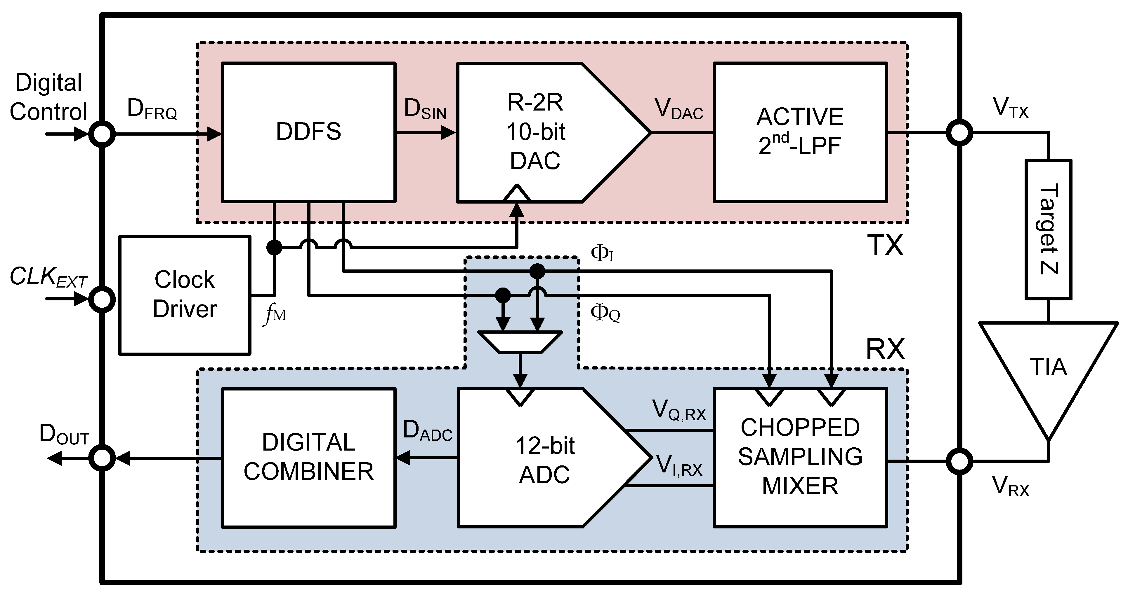
3.1. EIS Architecture Overview

Figure 2 illustrates the architecture of our sampling-mixer-based EIS SoC. The transmitter generates a programmable sinewave, which drives target impedance. The resulting current from the target is converted to voltage via an off-chip trans-impedance amplifier (TIA), which then drives the sampling-mixer-based on-chip receiver.
As mentioned above, the transmitter stage must generate a reference sinusoidal signal of a known and programmable frequency. To meet this need, a direct-digital frequency synthesis (DDFS) engine is implemented to generate a 10-bit digital sinewave. The DDFS runs at CLKEXT with fM = 50 MHz, and the frequency can be finely tunable with a 10-bit resolution. Since the digital sinewave is generated using CLKEXT, the highest frequency of the sinewave is less than fM. In our implementation, the DDFS can generate possible frequencies from fmin = 50 MHz/1024 to fmax = 25 MHz. Note that if we want to measure the target impedance at a lower frequency than fmin, we can lower the fM because the sinewave frequency is automatically scalable with the clock frequency. The DDFS is followed by a 10-bit DAC and a 2nd-order active low-pass filter that convert a digital sinewave into an analog one. The DAC adopts an R-2R DAC structure to reduce the number of resistor strings, thereby minimizing the area.
At the receiver side, the signal converted back to voltage through the TIA undergoes the sampling in the CMOS sampling mixer, where chopping is adopted to remove low-frequency noise such as flicker noise. In the sampling process, ΦI and ΦQ from the DDFS are used as the in-phase and the quadrature-phase sampling clock, respectively. Since these clocks are synchronized with the input signal, a quadrature sampling with the exact same frequency as the signal is realized. Moreover, to reduce the silicon area, a clock multiplexer is adopted so that either ΦI or ΦQ is routed to the sampling clock. By sequentially measuring the received signal at in-phase and quadrature-phase, it is possible to make all required measurements with a single ADC, which greatly saves the area. In addition, using the same ADC for sequential measurements fundamentally removes problems, such as offset and gain mismatches, that may occur when multiple ADCs are used. The ADC in the receiver is a wide-bandwidth pipeline Successive-Approximation-Register (SAR) ADC, the use of which makes extending both resolution and sampling speed much easier, compared to a conventional SAR ADC. In our design, the ADC operates at 5MS/s with a 12-bit resolution, both of which are necessary for wide-bandwidth and high-dynamic range measurement. The obtained 12-bit resolution output DADC is then further processed in an off-chip digital averaging filter with a window size of 4096 to enhance the dynamic range of the output.

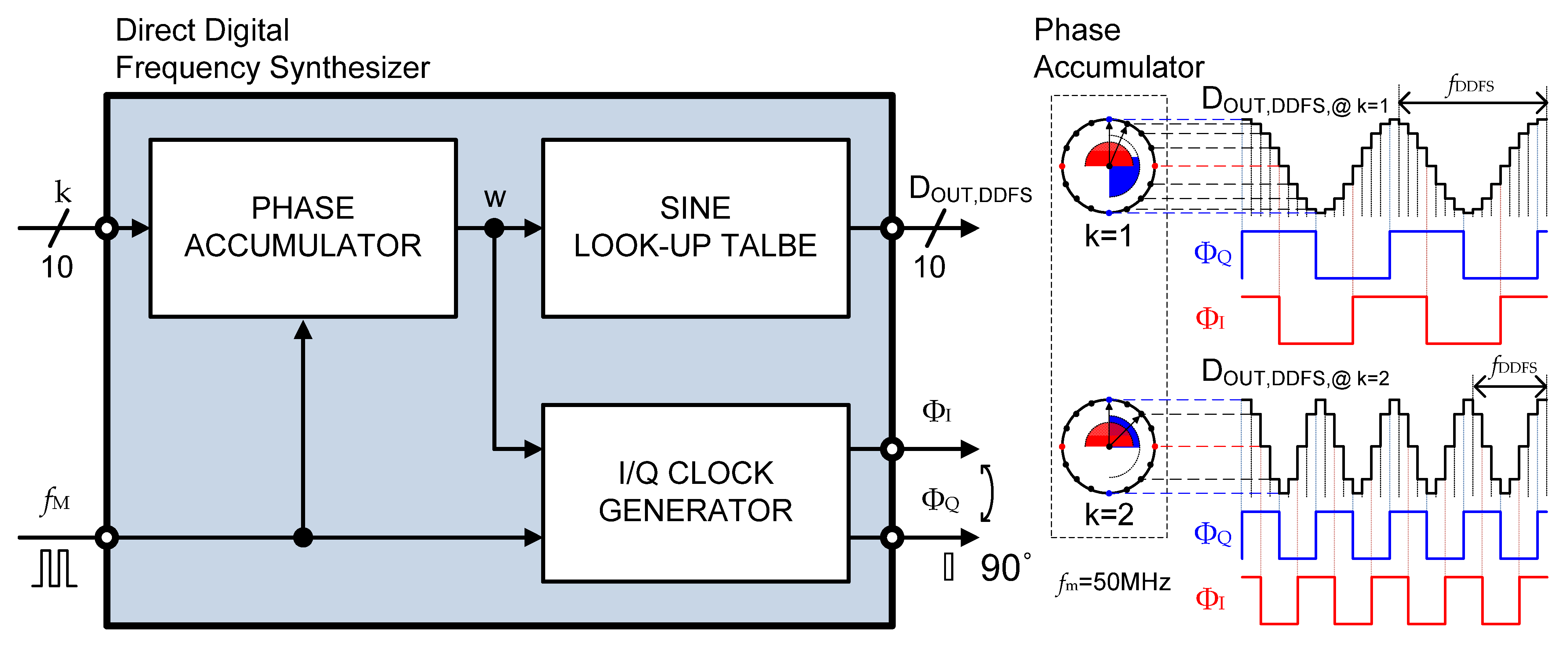
3.2. DDFS Implementation

Figure 3 illustrates the block diagram of the DDFS in the transmitter. In the transmitter, it is necessary to generate both the sinewave signal with a wide frequency range and the quadrature reference clock of the same frequency. A 10-bit DDFS is designed in this work, where the resolution is chosen to match with the following 10-bit D/A converter. The DDFS includes a digital phase accumulator that adds a fixed amount of phase for a sinewave at every DDFS clock cycle, a sine look-up table that stores the digital sinewave, and an I/Q clock generator that generates the in-phase and the clocks synchronized with the digital sinewave. When the DDFS clock frequency is f M , and the phase accumulator input is k, which is a programmable 10-bit digital accumulation step for the phase accumulator, the output frequency of the DDFS is given by
f D D F S = k 2 10 · f M .
This is accomplished by defining the look-up table to store the digital sinewave with a 10-bit phase resolution at intervals of 2π/1024. To generate the in-phase and quadrature-phase clock, the overall phase space is divided into four states on the phase boundaries at π/2, π, 3π/2, and 2π. By decoding these states, the DDFS generates two 90-degree shifted clocks. For example, the in-phase clock ΦI is a digital high when the DDFS phase is from 0 to π, and the quadrature-phase clock ΦQ is a digital high when the DDFS phase is between π/2 and 3π/2. This simple decoding logic allows us to build accurate quadrature clocks synchronized with signal frequency without using extra hardware.

3.3. EIS Receiver

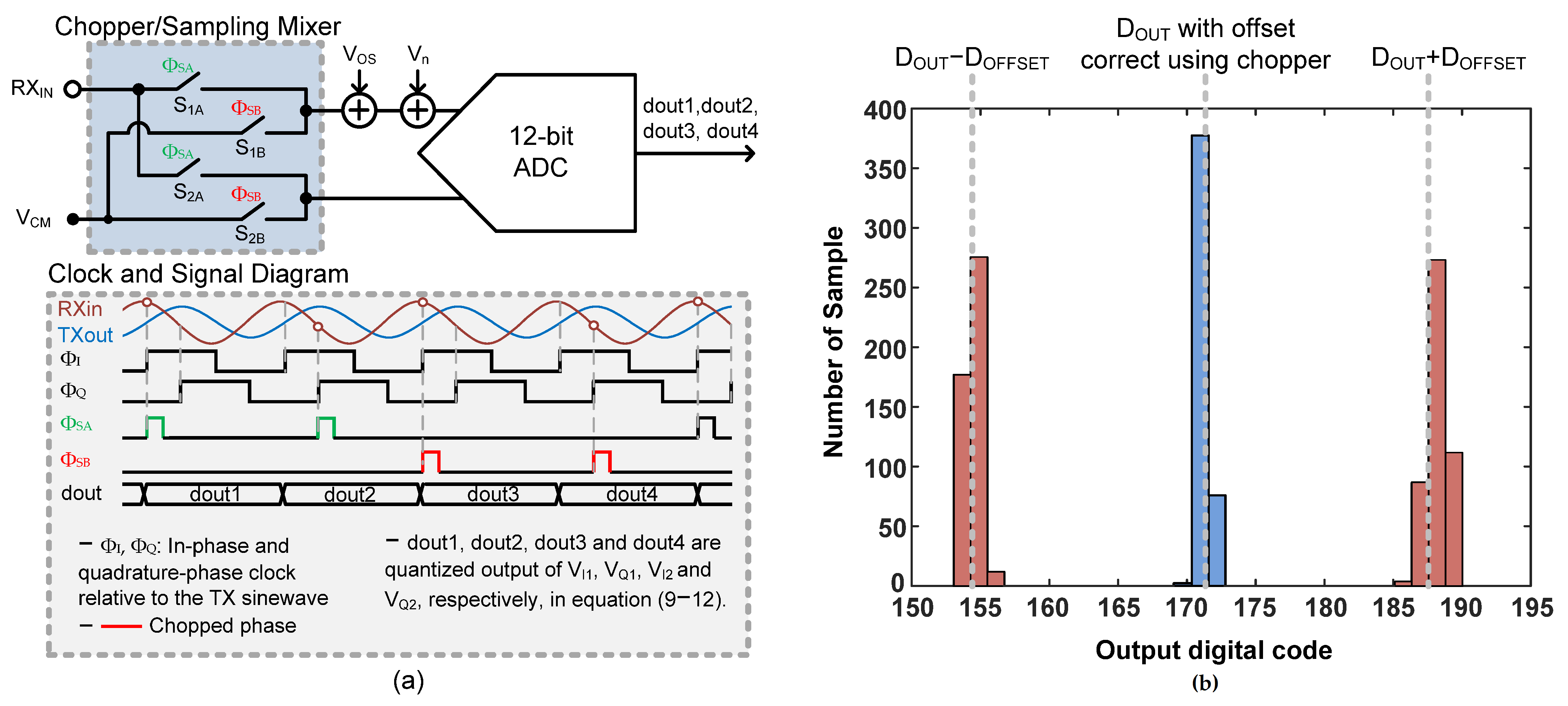
3.3.1. Chopped Sampling Mixer

Figure 4a shows the configuration of the chopped sampling mixer. As described in Section 2, it is necessary to detect the quadrature and in-phase components of the sine wave signal to calculate the magnitude and phase response. In other words, the receiver should be able to sample the signal quadrature voltage (VQ) and in-phase voltage (VI) with a phase difference of π/2. One concern here is that low-frequency noise, such as the flicker-noise of the switch or the input-referred offset of the ADC, can degrade the measurement accuracy because the signal is at DC. To alleviate this issue, a sampling mixer composed of four switches can be conceived, as illustrated in Figure 4. The switch operates in two configurations; when ΦSA is high, the switch S1A and S1B pair are connected to TIA output (denoted as RXIN) and common-mode voltage (VCM) to the differential input of the ADC. On the contrary, when ΦSB is high, the RXIN and VCM are swapped before being connected to the differential ADC input. Since this process needs to be performed twice for VQ and VI, respectively, the sampling and ADC operation are performed for a total of four cycles. Assuming that the total input-referred offset voltage ( V O S ) and low-frequency noise ( V n ) are added on the positive side of the ADC input, as shown in Figure 4, the four sampled values can be expressed as
V I 1 = V I , s a m + V O S + V n   ,
V Q 1 = V Q , s a m + V O S + V n   ,
V I 2 = V I , s a m + V O S + V n   ,
V Q 2 = V Q , s a m + V O S + V n   .
By combining (9), (10), (11), and (12), one can show that the resulting outputs are given by
V I = V I 1 V I 2 2 = V I , s a m ,
V Q = V Q 1 V Q 2 2 = V Q , s a m .
Therefore, it can be shown that the low-frequency noise and offsets are canceled out by the chopped sampler with the help of simple digital averaging.
Figure 4b shows the simulation result of a chopper with 50 mV DC input with sampling noise and 5 mV offset. The quantized DOUT value of 50 mV is 171, assuming a 12-bit ADC with 1.2 V input full scale. It is confirmed that the red bins that do not use the chopping technique show errors (about 17 in terms of digital output code). In contrast, the blue bins with chopping are centered around 171, where offset-included errors are removed.

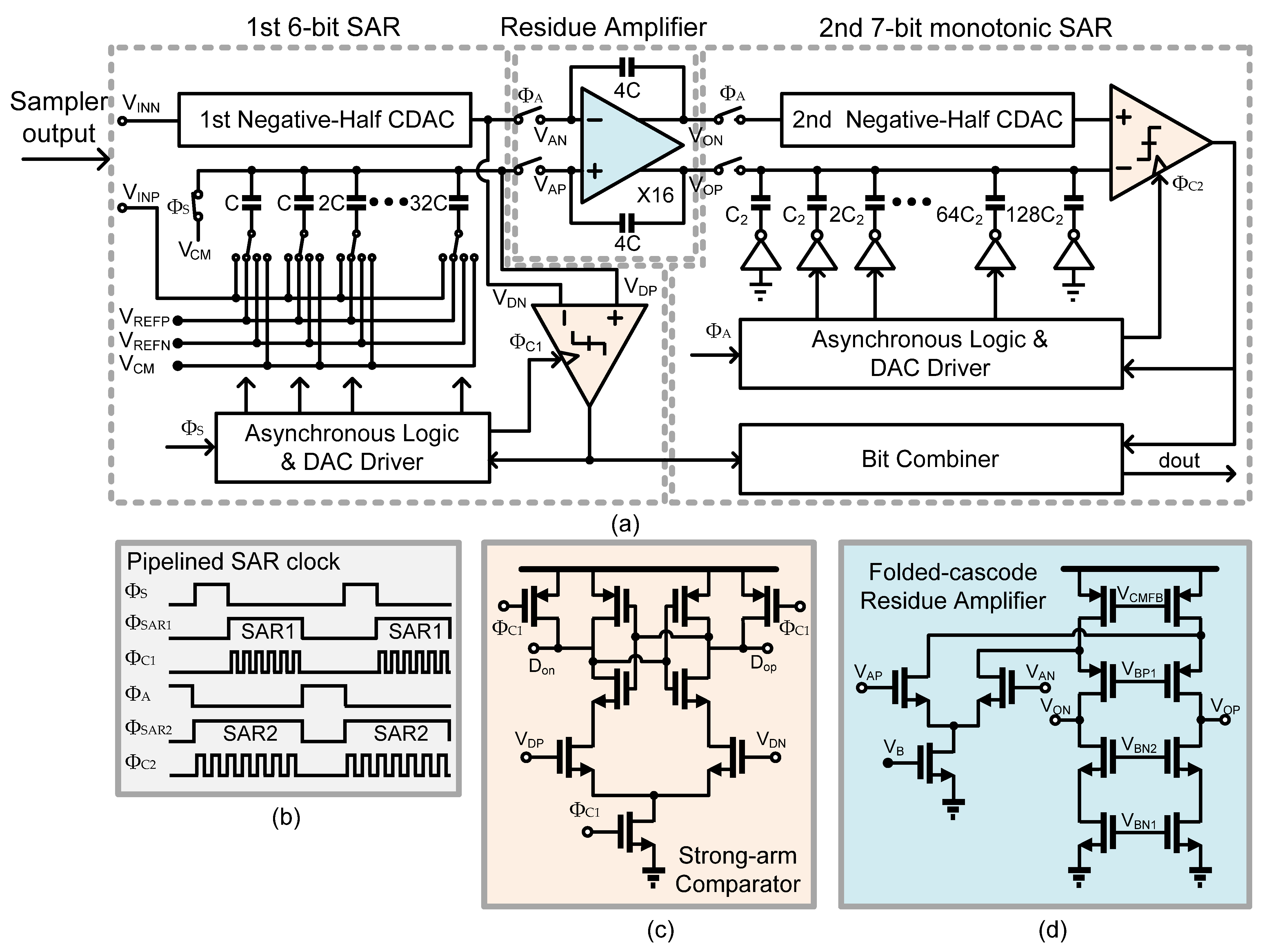
3.3.2. A 12-Bit 2-Stage Pipelined SAR ADC

The sampled voltage from the chopped sampling mixer needs to be converted to digital values for further post-processing. In this work, it is necessary to design an ADC with wide bandwidth and high resolution. A 12-bit, 2-stage pipelined SAR structure is chosen to satisfy the above design requirements. The overall block diagram and the schematics of the key circuits are shown in Figure 5a. The stage resolutions are 6-bit and 7-bit for the 1st and 2nd stage, respectively, and the inter-stage amplifier gain is chosen to be 16, considering the half-scale reference for the 2nd stage SAR ADC. This arrangement eases the amplifier design with a higher feedback factor while allowing the ADC to tolerate input referred offset of ±1/32 VREF in the 1st-stage SAR stage without degrading the overall ADC linearity. In addition, linearity errors of the ADC due to capacitor mismatch and parasitic capacitance are addressed by a foreground calibration from which we obtain optimal digital bit weights for the pipelined SAR ADC [14].
Figure 5b shows the clock diagram of pipelined SAR ADC. The clocking scheme improves ADC throughput by dividing the 12-bit conversions into ΦSAR1 and ΦSAR2 phases. Compared with a conventional 12-bit SAR ADC that would need 12 comparator clock cycles, the sampling speed of this ADC is improved by pipelining, which allows placing only six clock cycles for the first stage SAR and seven clock cycles for the second stage SAR, respectively.
The first stage 6-bit CDAC is implemented using a unit capacitance of 28 fF, leading to a total single-ended capacitance of 1.8 pF. A bottom-plate sampling method is adopted for the CDAC implementation, which is immune to the full-scale range reduction of the input stage. The control logic of the SAR ADC adopts asynchronous clocking to increase the power efficiency of the clock generator and is designed to be robust in metastability even in high-speed operation, where the conversion time is relatively fast. The comparator is designed using a strong-arm structure, as shown in Figure 5c.
The second stage 7-bit SAR ADC is designed slightly differently using a top-plate CDAC structure so that the first comparator cycle can be performed immediately after the sampling phase. The CDAC consists of 256 instances of the unit capacitors (C2), and the unit capacitance is about 4 fF. As mentioned earlier, to secure a 1-bit redundancy, 128 C2, which is half of the total capacitor, is used as a dummy capacitor so that the half reference is realized [15]. The control logic of the SAR ADC is designed as monotonic switching to minimize the CDAC switching power [16].
As shown in Figure 5d, the inter-stage residue amplifier is designed as a folded-cascode amplifier for a relatively large headroom while having a similar gain compared to the telescopic amplifier. The amplifier designed in 0.18- μ m CMOS process achieves a DC gain of 66 dB and unity gain bandwidth of 280 MHz according to SPICE simulations.
Figure 6 shows a simulation result of the 2-stage, 12-bit pipelined SAR ADC. Figure 6a shows the result of the residue transfer function of the inter-stage residue amplifier and the output voltage of the residue amplifier when a 1.2 V input differential voltage is applied. It confirmed that the residue transfer has a gain of 16, as expected. Note that the output of each line segment in the residue transfer must be sufficiently linear for the following-stage resolution, which is 7-bit in our case. The combined linearity has been verified by the time-domain ADC simulation. Figure 6b shows the simulated FFT of this ADC according to the SPICE simulator. The ADC achieves the SNDR of 67.99 dB with random noise enabled.

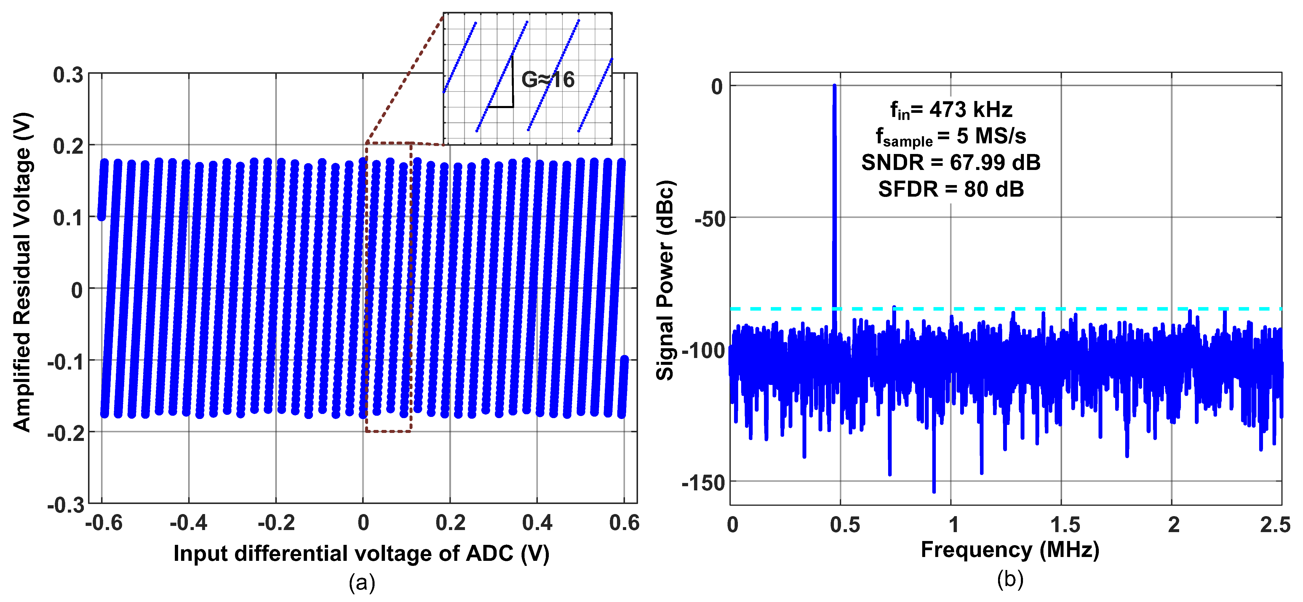
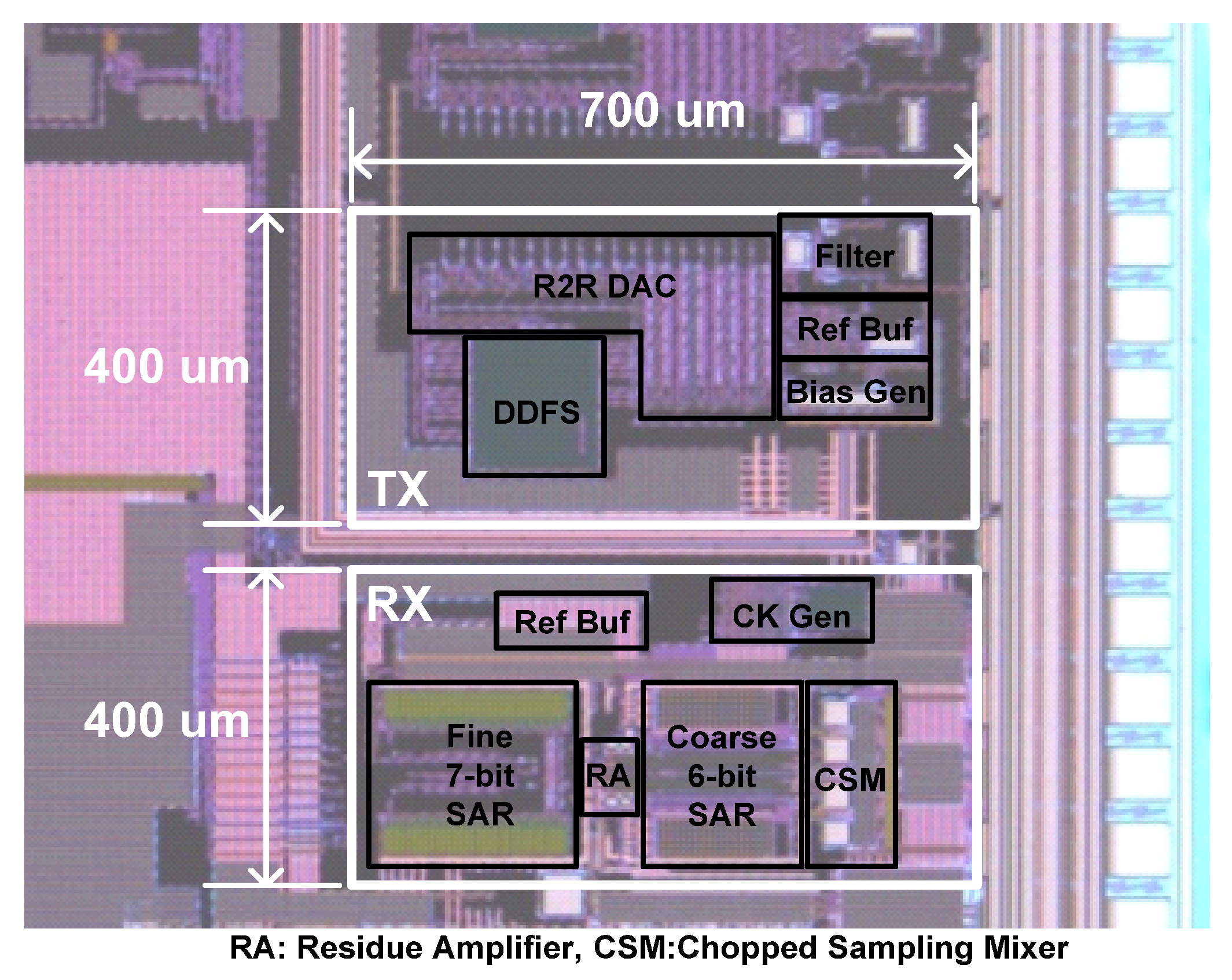
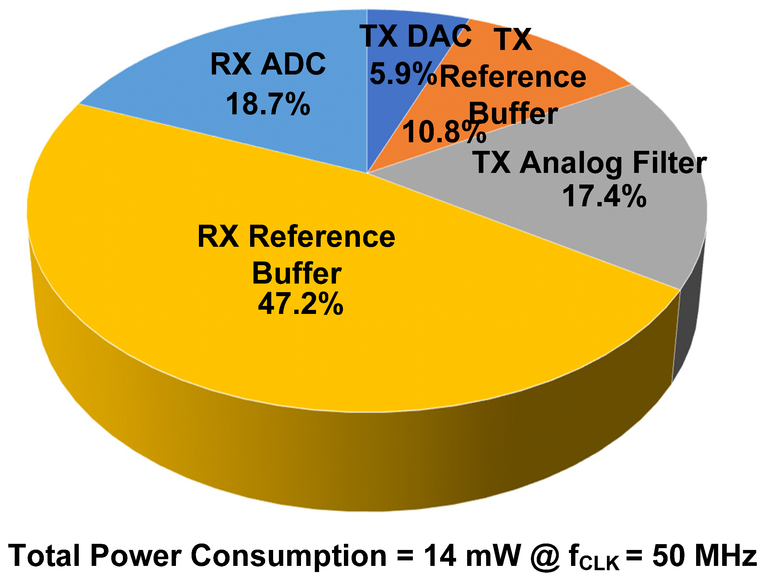
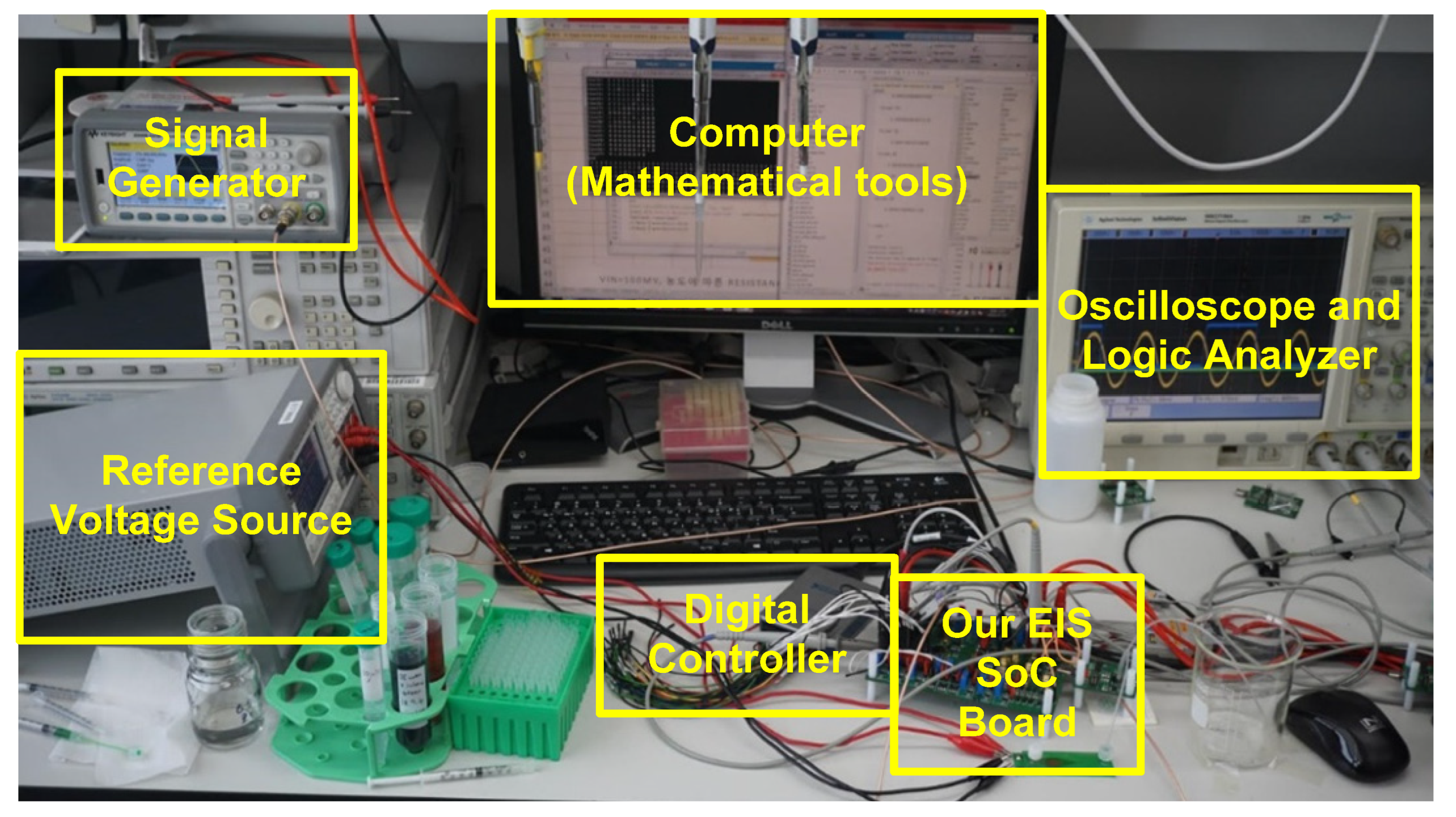
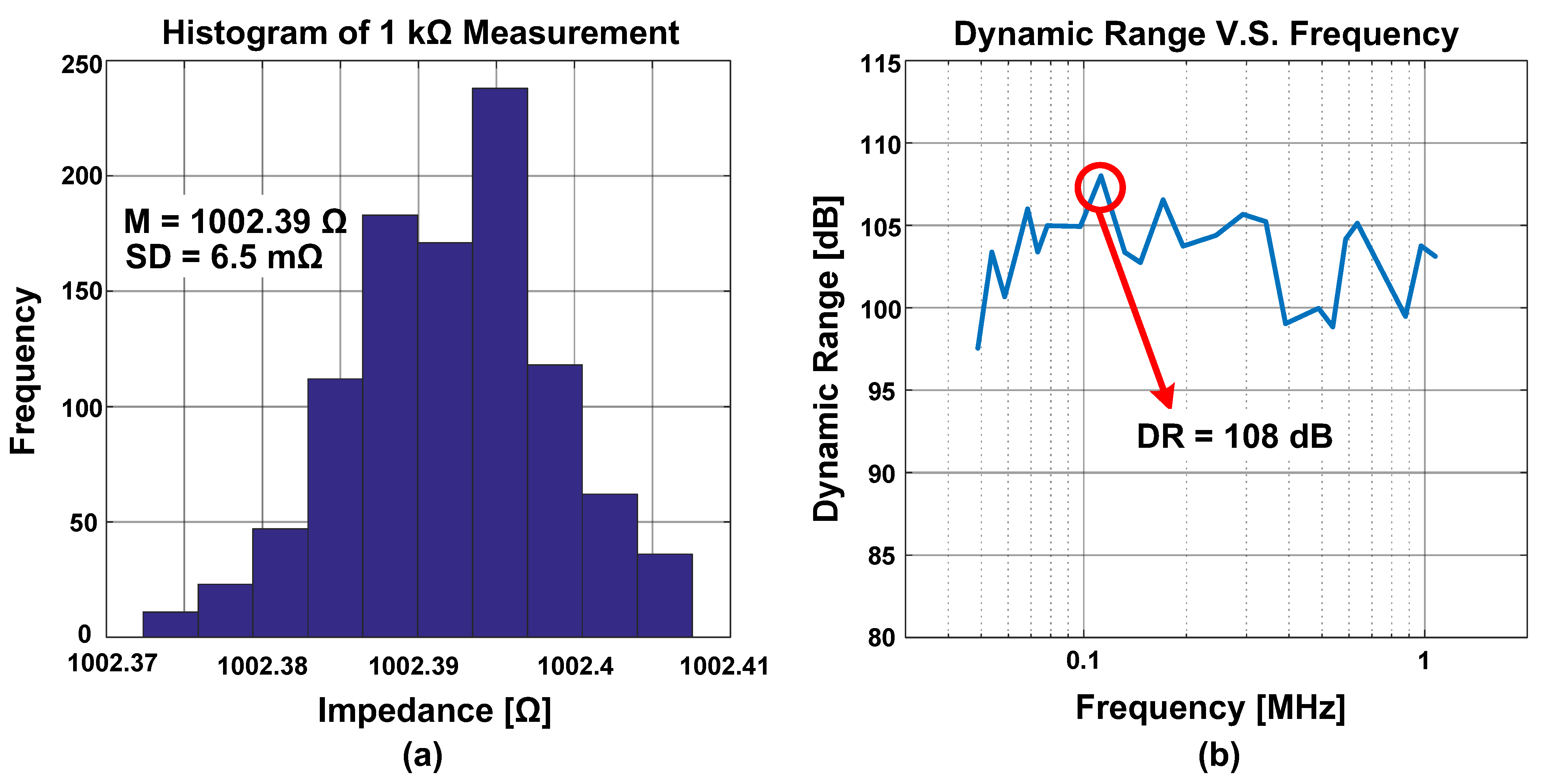
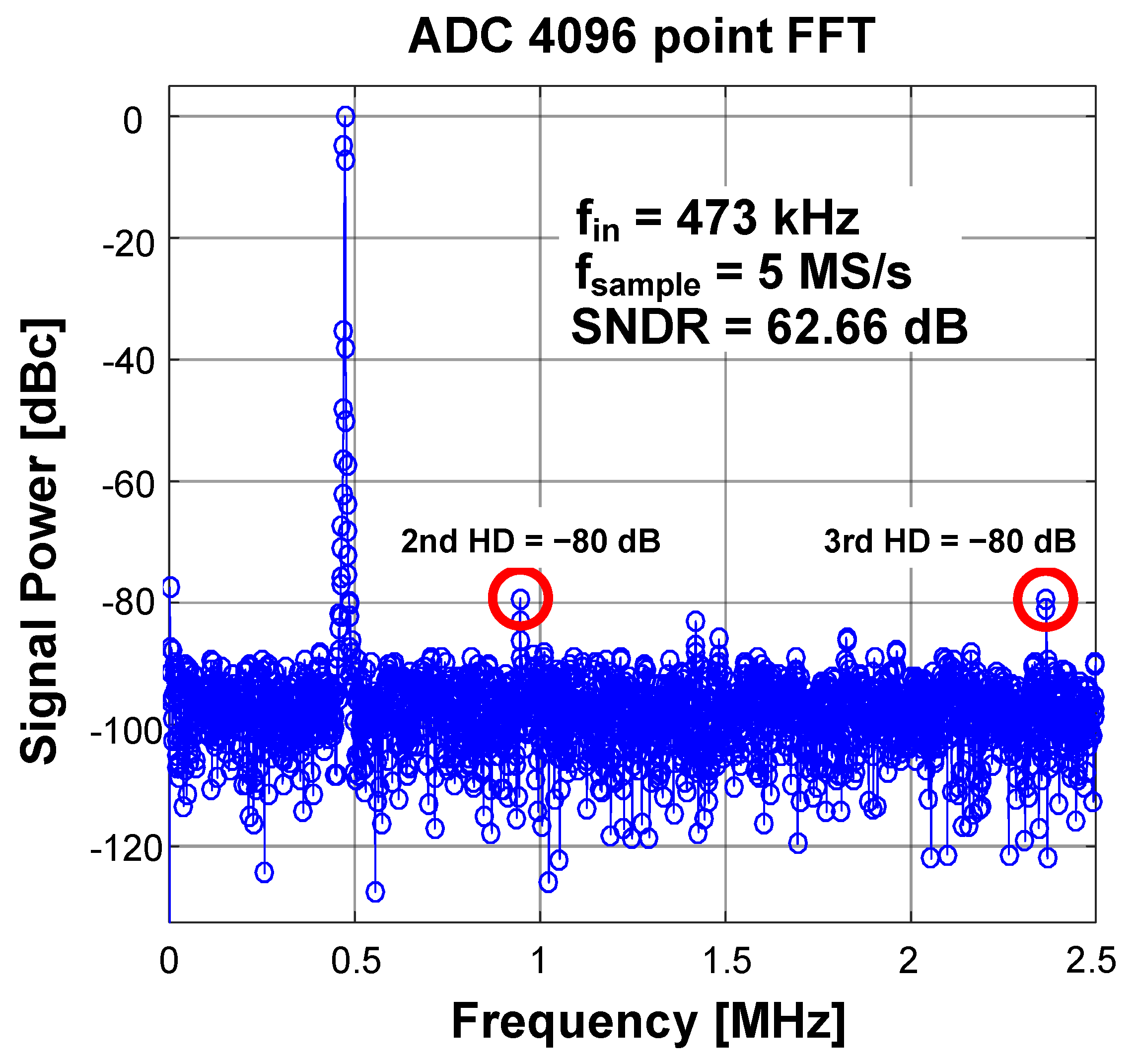
4. Measurement Results

Figure 7 shows the chip microphotograph of the EIS SoC. Fabricated in 0.18- μ m CMOS technology, the EIS core, including both the transmitter and the receiver, occupies an area of 0.56 mm2. The total power consumption is 14 mW when fM = 50 MHz and the detailed power breakdown is displayed in Figure 8. The EIS measurement setup is shown in Figure 9. The external 50 MHz clock is provided by an off-chip signal generator, and the digital control bits are programmed via an off-chip serial controller. The output of the transmitter drives an off-chip TIA with a feedback resistor, and the TIA output drives back to the input pad of the chip that is directly connected to the EIS receiver, including the chopped sampling mixer and the ADC. The output of the ADC is collected by a logic analyzer, which is further processed in a PC to calculate the impedance as described in Section 2.
The performance of this EIS was measured for a 1 k Ω target reference resistor. Shown in Figure 10a, the measured histogram of the digital output after the digital post-processing reveals that the RMS noise is 6.5 m Ω , which corresponds to a dynamic range of 108 dB. Figure 10b shows the result of measuring the dynamic range (DR) over a wide frequency range from 30 kHz to 1.25 MHz. The graph indicates that the worst-case DR is 97 dB, and the peak DR is 108 dB, as shown above. Figure 11 shows the measurement result of a stand-alone ADC mode via 4096-point FFT. Without the digital averaging, the ADC exhibits SNDR of 62.7 dB and SFDR of 80 dB for fin = 473 kHz and fsample = 5 MHz under 1.8 V supply.
Table 1 shows a comparison table that summarizes the performance of our EIS SoC with recently published state-of-the-art EIS papers. Total power dissipation is 14 mW, where the receiver and the transmitter consume 9.2 mW and 4.8 mW, respectively. This level of power consumption is comparable with other state-of-the-art works. In addition, thanks to the sampling-mixed-based topology, our EIS SoC achieves the largest EIS frequency scan range of 1.25 MHz while achieving the highest peak dynamic range of 108 dB.

5. Conclusions

This paper presented an electrochemical impedance spectroscopy chip with a measured peak dynamic range of 108 dB. The sampling-mixer-based prototype EIS SoC not only achieves a high dynamic range but also covers a wide frequency scan range from 30 kHz to 1.25 MHz without a need for quadrature sinewaves. The on-chip tunable DDFS provides both in-phase and quadrature-phase clocks with minimal extra digital logic. Thanks to the clever clocking scheme in the sampler, the quadrature measurement is achieved using a single 5 MS/s, 12-bit pipelined SAR ADC. The built-in chopper within the sampling mixer-based receiver reduces possible low-frequency noise in the sampler and input-referred offset of the ADC. With many demonstrated advantages, we believe that the presented EIS architecture can be used universally in various EIS measurements, and this architecture should easily be scalable to a design that demands an EIS frequency scan range over 100 MHz.

Author Contributions

H.K., H.L. and J.K. proposed architecture; H.K. and H.L. designed and simulated the circuit; H.K. performed all measurements; H.K. wrote the draft of the manuscript and J.K. supervised the manuscript. All authors have read and agreed to the published version of the manuscript.

Funding

This research was supported by Basic Science Research Program through the National Research Foundation of Korea (NRF) funded by the Ministry of Education (2020R1F1A1067414), and by Institute of Information & Communications Technology Planning & Evaluation (IITP) grant funded by the Korea government (MSIT) (No. 2022-0-01171, A Development of Intelligent PHY Interface for High-Speed PIM Data Transfer).

Acknowledgments

The authors thank IDEC for CAD tool support.

Conflicts of Interest

The authors declare no conflict of interest.

Appendix A

Figure 1c shows the simple lock-in detection block diagram where V i n ( t ) and V r e f ( t ) are sinusoidal signals having the same frequency. The V i n ( t ) is a signal whose amplitude ( A 0 ) and phase ( φ ) are unknown, except for the angular frequency ( ω ). These two signals can then be expressed as
V i n ( t ) = A 0 · sin ( ω t + φ ) ,
V r e f ( t ) = A r · sin ( ω t ) .
Suppose that the V i n ( t ) in (A1) passes through the gain of G. To detect the A 0 and φ output, we can multiply V i n ( t ) by both the in-phase and quadrature-phase sinewave of V r e f ( t ) , which leads to
V 1 ( t ) = 1 2 G A 0 A r { cos ( φ ) cos ( 2 ω t + φ ) } ,
V 2 ( t ) = 1 2 G A 0 A r { sin ( 2 ω t + φ ) + sin ( φ ) } .
By applying low-pass filters to V 1 ( t ) and V 2 ( t ) individually and multiplying a scaling factor of 2 / G A R , one can easily show that the outputs are given by
V I = A 0 sin ( φ )
V Q = A 0 cos ( φ )
Finally, by performing simple mathematical operations shown below, both the magnitude and phase of the V i n ( t ) can be obtained, i.e.,
A 0 = V Q 2 + V I 2 ,
φ = tan 1 ( V I V Q )

References

  1. Qu, G.; Wang, H.; Zhao, Y.; O’Donnell, J.; Lyden, C.; Liu, Y.; Ding, J.; Dempsey, D.; Chen, L.; Bourke, D.; et al. A 0.28 mΩ-Sensitivity 105 dB-Dynamic-Range Electrochemical Impedance Spectroscopy SoC for Electrochemical Gas Detection. In Proceedings of the 2018 IEEE International Solid-State Circuits Conference (ISSCC), San Francisco, CA, USA, 11–15 February 2018; pp. 286–288. [Google Scholar]
  2. Chen, C.H.; Liu, J.; Amine, K. Symmetric cell approach and impedance spectroscopy of high power lithium-ion batteries. J. Power Sources 2001, 96, 321–328. [Google Scholar] [CrossRef]
  3. Fosbøl, M.Ø.; Zerahn, B. Contemporary methods of body composition measurement. Clin. Physiol. Funct. Imaging 2015, 35, 81–97. [Google Scholar] [CrossRef] [PubMed]
  4. Hafid, A.; Benouar, S.; Kedir-Talha, M.; Abtahi, F.; Attari, M.; Seoane, F. Full Impedance Cardiography measurement device using Raspberry PI3 and System-on-Chip biomedical Instrumentation Solutions. IEEE J. Biomed Health Inform. 2018, 22, 1883–1894. [Google Scholar] [CrossRef] [PubMed]
  5. Kim, M.; Kim, H.; Jang, J.; Lee, J.; Lee, K.; Kim, K.; Lee, Y.; Yoo, H.J. A 1.4 mΩ-sensitivity 94 dB-dynamic-range electrical impedance tomography SoC and 48-channel Hub SoC for 3D lung ventilation monitoring system. In Proceedings of the 2017 IEEE International Solid-State Circuits Conference (ISSCC), San Francisco, CA, USA, 5–9 February 2017; pp. 354–355. [Google Scholar]
  6. Lopez, C.M.; Chun, H.S.; Berti, L.; Wang, S.; Putzeys, J.; Bulcke, C.V.D.; Weijers, J.W.; Firrincieli, A.; Reumers, V.; Braeken, D.; et al. A 16384-Electrode 1024-Channel Multimodal CMOS MEA for High-Throughput Intracellular Action Potential Measurements and Impedance Spectroscopy in Drug-Screening Applications. In Proceedings of the 2018 IEEE International Solid-State Circuits Conference (ISSCC), San Francisco, CA, USA, 11–15 February 2018; pp. 464–466. [Google Scholar]
  7. Manickam, A.; Singh, R.; McDermott, M.W.; Wood, N.; Bolouki, S.; Naraghi-Arani, P.; Jhonson, K.A.; Kuimelis, R.G.; Schoolnik, G.; Hassibi, A. A Fully Integrated CMOS Fluorescence Biochip for DNA and RNA Testing. IEEE J. Solid-State Circuits 2017, 52, 2857–2870. [Google Scholar] [CrossRef] [PubMed]
  8. Velmanickam, L.; Pokharel, R.; Lima, I.T.; Nawarathna, D. Label Free MicroRNA Biomarker Detection in Serum Samples for Diagnosis Applications at Point-of Care. In Proceedings of the 2019 IEEE Research and Applications of Photonics in Defense Conference (RAPID), Miramar Beach, FL, USA, 19–21 August 2019; pp. 1–4. [Google Scholar]
  9. Sui, J.; Gandotra, N.; Xie, P.; Lin, Z.; Scharfe, C.; Javanmard, M. Multi-frequency impedance sensing for detection and sizing of DNA fragments. Sci. Rep. 2021, 11, 6490. [Google Scholar] [CrossRef] [PubMed]
  10. Kim, Y.; Goo, S.-G.; Lim, J.S. Multi-Gas Analyzer Based on Tunable Filter Non-Dispersive Infrared Sensor: Application to the Monitoring of Eco-Friendly Gas Insulated Switchgears. Sensors 2022, 22, 8662. [Google Scholar] [CrossRef] [PubMed]
  11. Manickam, A.; Johnson, C.A.; Kavusi, S.; Hassibi, A. Interface Design for CMOS-Integrated Electrochemical Impedance Spectroscopy (EIS) Biosensors. Sensors 2012, 12, 14467–14488. [Google Scholar] [CrossRef] [PubMed] [Green Version]
  12. Masciotti, J.M.; Lasker, J.M.; Hielscher, A.H. Digital Lock-In Detection for Discriminating Multiple Modulation Frequencies With High Accuracy and Computational Efficiency. IEEE Trans. Instrum. Meas. 2008, 57, 182–189. [Google Scholar] [CrossRef]
  13. Pekau, H.; Haslett, J.W. A 2.4 GHz CMOS sub-sampling mixer with integrated filtering. IEEE J. Solid-State Circuits 2005, 40, 2159–2166. [Google Scholar] [CrossRef]
  14. Yoon, J.S.; Kim, J. An Efficient Digital-Domain Calibration Technique for SAR ADCs Using a Bridge Capacitor. J. Semicond. Technol. Sci. 2019, 19, 79–86. [Google Scholar] [CrossRef]
  15. Lee, C.C.; Flynn, M.P. A SAR-Assisted Two-Stage Pipeline ADC. IEEE J. Solid-State Circuits 2011, 46, 859–869. [Google Scholar] [CrossRef]
  16. Liu, C.C.; Chang, S.J.; Huang, G.Y.; Lin, Y.Z. A 10-bit 50-MS/s SAR ADC With a Monotonic Capacitor Switching Procedure. IEEE J. Solid-State Circuits 2010, 45, 731–740. [Google Scholar] [CrossRef]
  17. Kim, K.; Kim, J.H.; Gweon, S.; Kim, M.; Yoo, H.J. A 0.5-V Sub-10-μW 15.28-mΩ/√Hz Bio-Impedance Sensor IC With Sub-1° Phase Error. IEEE J. Solid-State Circuits 2020, 55, 2161–2173. [Google Scholar] [CrossRef]
Figure 1. Simple measurement system of Vin with (a) only an amplifier, (b) an amplifier with a bandpass filter, and (c) an amplifier and lock-in detection block.
Electronics 11 04130 g001
Figure 2. The block diagram of our EIS SoC.
Electronics 11 04130 g002
Figure 3. The DDFS block diagram with a principle of DDFS operation.
Electronics 11 04130 g003
Figure 4. (a) The block diagram of a chopped sampling mixer along with key waveforms. (b) The simulation result of offset cancellation using a chopping technique.
Electronics 11 04130 g004
Figure 5. (a) The architecture of the 12-bit pipelined SAR ADC. (b) The clock diagram of the pipelined SAR ADC. (c) The comparator. (d) The stage residue amplifier using a folded-cascode structure.
Electronics 11 04130 g005
Figure 6. (a) The simulated residue transfer function of 2-stage pipelined SAR ADC. (b) The simulated ADC spectrum with 473 kHz input when random noise is enabled.
Electronics 11 04130 g006
Figure 7. Die photograph of our EIS SoC.
Electronics 11 04130 g007
Figure 8. Power breakdown of our EIS SoC at 50 MHz.
Electronics 11 04130 g008
Figure 9. Measurement setup of our EIS system.
Electronics 11 04130 g009
Figure 10. (a) Histogram of measured impedance over 1000 measurements. (b) Dynamic range measurement from 30 kHz to 1.25 MHz.
Electronics 11 04130 g010
Figure 11. ADC output spectrum with 473 kHz input in stand-alone mode.
Electronics 11 04130 g011
Table 1. Performance comparison table.
FeaturesThis WorkISSCC 18 [1]ISSCC 17 [5]ISSCC 18 [6]JSSC 20 [17]
Technology180 nm180 nm65 nm130 nm65 nm
Dynamic Range108 dB105 dB94 dBUnknown76.32 dB
Power14 mW20.6 mW6.69 mW95 mW9 mW
Operating Frequency Range1.25 MHz200 kHz128 kHz1 MHz408 kHz
Frequency TunabilityTunableTunableTunableN/ATunable
ADC Structure12-bit pipelined SAR16-bit SAR12-bit SAR10-bit SARNot included
Publisher’s Note: MDPI stays neutral with regard to jurisdictional claims in published maps and institutional affiliations.

