Article

A Compact Model for Single-Event Transient in Fully Depleted Silicon on Insulator MOSFET Considering the Back-Gate Voltage Based on Time-Domain Components

1
Institute of Microelectronics of Chinese Academy of Sciences, Beijing 100029, China
2
Key Laboratory of Science and Technology on Silicon Device, Chinese Academy of Sciences, Beijing 100029, China
3
University of Chinese Academy of Sciences, Beijing 100029, China
*
Authors to whom correspondence should be addressed.
Electronics 2022, 11(23), 4022; https://doi.org/10.3390/electronics11234022
Submission received: 3 November 2022 / Revised: 1 December 2022 / Accepted: 2 December 2022 / Published: 4 December 2022
(This article belongs to the Section Microelectronics)

Abstract

:
FDSOI (Fully Depleted Silicon On Insulator) devices have a good performance in anti-single-event circuits. However, the bipolar amplification effect becomes a severe problem due to the buried oxide. The previous models for Single Event Transient (SET) of FDSOI did not fully consider the current of all components. Most importantly, they did not take the influence of the back-gate voltage into account. Thus, this paper presents a modeling method for the SET current in FDSOI MOSFET where all three components are modeled individually. The prompt current and diffusion current are modeled with a current source respectively. The Berkeley Short-channel IGFET Model for Silicon-on-Insulator (BSIMSOI) model is integrated into this model to calculate the bipolar amplification current. Compared to using the bipolar transistor model, this method avoids additional current input from the base electrode. It is more consistent with the mechanism of bipolar amplification effect for FDSOI devices without body contact. Instantaneously, an improved model is proposed that considers the influence of the back-gate voltage on the SET of the FDSOI devices. All models are validated through Technology Computer Aided Design (TCAD)simulation results.

1. Introduction

Soft error induced by single event effect is a serious issue in advanced CMOS logic VLSI (very large-scale integration) [1,2,3]. For FDSOI MOSFET, the fully dielectric isolated structure prevents the circuit from latch-up effects. However, it can also cause severe Bipolar Amplification Effects (BAE) [4,5,6]. The charge collection of the stroked node could be much larger than the total charge accumulated by the heavy ion because of the bipolar amplification current. Then, a sensitive node in the off state may flip up due to this effect. Meanwhile, TCAD simulation shows that the strength of the Single Event Transient (SET) current could be modulated by back-gate voltage. An accurate compact model for the SET current of FDSOI devices is essential in the design of anti-single-event circuits.
The double exponential transient model is wildly used in circuit simulation of the single event effect [7,8]. However, many works have pointed out that this model could not be wide enough compared with the real transient pulse [9,10,11]. It is because this model is derived based on that the depletion region of a reverse-biased PN junction is stroked by a heavy ion [12]. The drift of the ionized carriers is its main consideration, and the diffusion effect is ignored in this model, although some work has been performed to improve it, such as using multiple double exponential functions to expand the width of the transient [9]. This method weakens the physical background of the model and increases the fitting parameters exponentially. Therefore, there is an urgent need to establish a more suitable SET model from the mechanism of the single event effect of MOSFET devices.
The SET current in the FDSOI MOSFET device can be decomposed into three components in the time domain [13]. Some work has been to model different components of the FDSOI device SET current. For instance, David et al. presented a SET model considering carrier diffusion and the parasitic bipolar transistor [14]. However, they did not distinguish the diffusion current from the prompt current. Rostand et al. computed the bipolar amplification current by transferring the concentration of the holes in the body to the concentration of electrons in the channel due to the BAE through the use of an empirical function [15]. However, the function to calculate the bipolar amplification current, after reaching the concentration of electrons, is too simple to obtain a convincing result. Furthermore, only two components of the SET current of the FDSOI device are considered in their model. Another important issue is that none of these models have taken the influence of the back-gate voltage into account.
Thus, this paper presents a modeling method for the SET of FDSOI MOSFET. All three components are modeled respectively, and their relationships are considered. In the modeling of the bipolar amplification current, the body potential is calculated and introduced into the integrated BSIMSOI model as this current is directly related to the device model. This approach avoids the problem that the floating body FDSOI device does not have a corresponding base electrode when using the bipolar transistor model to calculate the bipolar amplification currents.
Meanwhile, an improved model is proposed too, considering the effect of the back-gate voltage on the SET of the FDSOI devices. These models are SPICE compatible and validated through TCAD simulation results.
To sum up, the paper will be divided as follow: in section II, the TCAD simulation details as well as the discussion of the results will be proposed. Section III presents the modeling of the SET current, and the consideration of the back-gate voltage is introduced in section IV. Finally, a conclusion will sum up this work.

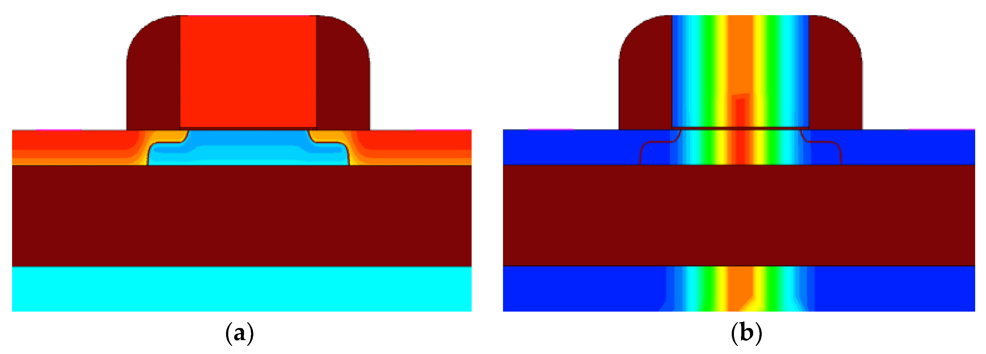
2. TCAD Simulation Details and Result Discussion

The structure of FDSOI, used in the 2D TCAD simulation, is presented in Figure 1a where the gate length L is equal to 0.18 μm, the top silicon thickness Tsi is equal to 50 nm, and the thickness of buried oxide Tbox is equal to 145 nm. The heavy ion penetrates the device perpendicularly in the middle of the gate at the off state with 1 μm track length, 80 nm track width, 0.4 pC/μm of Leaner Energy Transfer (LET) value, and a Gaussian distribution of the induced ehps. The LET value along the track has been considered fixed as shown in Figure 1b.
The simulation results are shown in Figure 2. The SET current of the FDSOI devices can be decomposed into three parts:
-
The first one is the prompt current. This current is formed by the ionized electrons around the PN junction between the body and the drain leaving more holes than electrons in the body. This process will increase the body’s potential and cause the bipolar amplification effect;
-
The second one is the diffusion current formed by the diffusion of the ionized electrons that still remain in the body. The diffusion current of the ionized holes will be collected by the source. As carrier diffusion proceeds, the difference in concentration between ionized holes and electrons in the body decreases, and the bipolar amplification effect diminishes instantaneously;
-
The third one which is the largest part is the bipolar amplification current. It represents a drift current from the source to the drain caused by the BAE.

3. Modeling of SET Current

An equivalent sub-circuit of this model has been shown in Figure 3. Each of the prompt current and the diffusion currents is modeled using a current source. In the bipolar amplification current model, the total net charge in the body is calculated and transformed into the body potential by using an experimental capacitance. The body potential is viewed as a voltage source connected to a virtual body electrode in order to change the threshold voltage of the BSIMSOI compact model to simulate the bipolar amplification effect. The model parameter of BSIMSOI has been extracted from TCAD simulation results. As for the bipolar amplification current, it will be calculated from the integrated BSIMSOI model and it will be considered equal to the drain current.

3.1. Modeling of Prompt Current

When a heavy ion strikes the body region of the device, several electron-hole pairs will be generated and distributed in the whole body in a short time. Under this condition, the electric field in the PN junction will be disturbed and the depletion region of the PN junction between the body and the drain will be shortened and then partially recovered as shown in Figure 4. This is due to electron collection of the drain. The prompt current corresponds to this process, and it can be abstracted as a charging and discharging process of a capacitor related to the depletion region and the distribution of the ionized charge. The equivalent circuit is shown in Figure 5a where the voltage source is a non-idea one and Rp is the resistance of the circuit. The voltage source needs a period of time (Tp) to reach its steady value as shown in Figure 4b. The Tp parameter corresponds to the time required for the depletion region the shrink to the minimum length. Rp and Cp should be variables changing with the concentration and the distribution of the ionized charge. For simplicity, they are all assumed to be constants. The current response of the voltage source is represented in Equation (1) and the curve is shown in Figure 5b where U s = V d s / T p , and τ = R p C p . The fitting result of this model has been displayed in Figure 6 along with the diffusion current model.
I prompt = C p U s C p U s exp t τ t < T p C p U s exp T p τ C p U s exp t τ t T p

3.2. Modeling of Diffusion Current

The electrons that escaped from the body through the prompt current just represent a small fraction of the total ionized electrons. There are still many ionized electrons and whole ionized holes remaining in the body. Diffusion will be their main transport mechanism to leave the body. Few of the electrons and the holes may recombine with each other; thus, they are not considered in this model.
The diffusion of the carriers in the body obeys the diffusion function represented in Equation (2) where N is the carrier concentration, x is the radius of the charge cloud and D is the bipolar diffusion coefficient. In high injection conditions, the holes and the electrons will share the same diffusion coefficient D.
The relationship between the ambipolar diffusion coefficient and the normal diffusion coefficient of electrons (Dn) and holes (Dp) is shown in Equation (3) where n and p represent the concentration of electrons and holes in the body, respectively, and μn and μp represent the mobility of the electrons and the holes, respectively. Due to the presence of the PN junctions at both ends of the body region, the diffusion of the carriers is subjected to boundary conditions which are shown in Equation (4). The drain is defined at l = 0, and the source at l = L, where N(l,t) represents the carrier concentration at position l and at time t.
D 2 N N 2 = N t
D = ( n + p ) D n D p n D n + p D p
N ( 0 , t ) = 0 N ( 0 , 0 ) = 0 N ( L , 0 ) = 0
The diffusion of the charge cloud in the body has three stages:
(1)
at the beginning, the cloud shape is Gaussian because of free diffusion;
(2)
the Gaussian distribution will be transformed to an approximately “linear” shape after the cloud collides with the source and the drain junction;
(3)
the “linear” cloud decays because of the discharge of the source hole current and the drain electron current [14].
For stages (2) and (3), the solution of the diffusion function for electrons is presented in Equations (5)–(10) [14]. Where d is the thickness of the top silicon film, wb is the device width, q is the charge of an electron, and β is a parameter related to the emitter efficiency which is used as a fitting parameter in this model. Added to that, Qelec is the total charge of electrons participating in diffusion as shown in Equation (10). The diffusion current of electrons yields as proposed in Equation (11).
N e l e c t r o n ( x , t ) = 2 Q e l e c q d w b L a n { e t / τ 1 n sin [ a n x / L ] + 0.5 e t / τ 2 n sin [ ( 2 π a n ) x / L ] 0.5 e t / τ 3 n sin [ ( 2 π + a n ) x / L ] } ,  
a n = [ 2 ( D n / D p + 1 ) / β ] 1 / 2 ,  
τ 1 n = β L 2 4 D n ,  
τ 2 n = L 2 D ( 2 π a n ) 2 ,  
τ 3 n = L 2 D ( 2 π + a n ) 2 ,  
Q e l e c = L E T × d I p r o m p t d t = L E T × d C p U s T p ,  
I d i f f u s i o n ( t ) = 2 w b d q D n N e l e c t r o n ( 0 , t ) = 4 D n Q e l e c L 2 a [ a n e t / τ n 1 + 0.5 ( 2 π a n ) e t / τ n 2 0.5 ( 2 π + a n ) e t / τ 3 n ] ,  
The fitting result of the diffusion current model is displayed in Figure 6. In this model, the diffusion coefficient of electrons and the holes in the high injection condition should be extracted.
As the diffusion current can only be detected after the charge cloud collides with the PN junction, Equation (11) in the SPICE model requires a delay time (Td); thus, this parameter needs to be extracted.

3.3. Modeling of Bipolar Amplification Current

Under high injection conditions, the diffusion current of holes (Ihdiffusion) is almost the same as the diffusion current of electrons (Idiffusion) due to the bipolar diffusion effect. Ihdiffusion is slightly larger than the Idiffuson because there are more holes in the body. The diffusion of the net charge from the body could be modeled with the same diffusion model as shown in Equations (12) and (13), where the parameter of the electrons and the holes should be swapped.
I d i s c h a r g e ( t ) = 2 w b d q D p q ( 0 , t ) = 4 D p Q n e t L 2 a p [ a p e t / τ p 1 + 0.5 ( 2 π a p ) e t / τ p 2 0.5 ( 2 π + a p ) e t / τ p 3 ] ,  
Q n e t = I p r o m p t d t = C p U s T p ,  
Considering that the prompt current is viewed as the charging process of the net charge in the body, the change of the total net charge in the body can be expressed as shown in Equation (14). As there are still some holes that will drift from the body to the source, and for simplicity, a constant parameter Idr is introduced into Equation (14) to represent the drift current. The fitting result of the net charge in the body is shown in Figure 7.
Q n e t = [ I p r o m p t ( t ) + I d i s c h a r g e ( t ) + I d r ] d t ,  
The body voltage Vb could be transformed from the total net charge in the body by using a capacitance Cb as proposed in Equation (15) where Cb is not just a constant. The experimental expression is thus presented in Equation (16):
V b = Q n e t / C b ,  
C b = C 1 + k 1 t 1 + e k 2 ( t t c b ) ,  
where C1, k2, and tcb, are the fitting parameters.
In some previous models [14,16], the bipolar transistor model was used to simulate the parasitic bipolar transistor. However, in the bipolar transistor model, the base is directly connected to the outside which may induce the extra base current into the device. This method is not appropriate for FDSOI devices without body contact.
In this work, the BSMSOI model was used to calculate the bipolar amplification current. Its original body electrode is floating. The body voltage Vb is considered as a voltage source connected to a virtual body electrode of the device which has been already shown in Figure 3. This voltage source will change the threshold voltage of the device to calculate the drain current; however, it will not input or output any current from it just as the BAE dose in the FDSOI device.
Under normal conditions, the relationship between the body voltage and the threshold voltage (Vth) could be expressed using Equation (17) where Vfb is the flat band voltage, ψ B is the Fermi potential, ε s i   is the dielectric constant of silicon, Na is the doping concentration and Cox is the capacitance of the front oxide. However, with the ion strike, the body voltage could be much larger than the surface potential, so Equation (17) is not valid anymore. In this work, a more concise expression has been adopted and it is represented in Equation (18) where V t h B S I M is the threshold voltage of the original BSIMSOI model, V t h S E E is the new threshold voltage affected by the Vb, and kvb is a fitting parameter. In fact, V t h S E E will replace V t h B S I M to help in the calculation of the drain current in the BSIMSOI model.
V t h = V f b + 2 ψ B + 2 ε s i q N a ( 2 ψ B V b ) C o x ,  
V t h S E E = V t h B S I M k v b V b ,  
The bipolar amplification current can be expressed as shown in Equation (19). The parameters of BSIMSOI have been extracted from the TCAD simulation results. In addition, in circuit simulation, the parameters of the integrated BSIMSOI model should be in line with the model parameter of the device which was assumed to be struck by heavy ions. Therefore, if the parameters related to process fluctuations for different locations of the wafer have been extracted, these fluctuations will also be reflected in the simulation of the SET currents.
I b i p o l a r = I d s B S I M S O I ( V t h S E E ) ,  
The fitting result of the bipolar amplification current is presented in Figure 8.
The final SET current could be yielded as proposed in Equation (20) which represents the sum of the three components. The result are displayed in Figure 9.
I S E T = I p r o m p t + I e d i f f u s i o n + I b i p i l a r ,  

4. Model Considering the Back-Gate Voltage

TCAD simulation results show that the SET of the FDSOI device could be modulated by the back gate voltage as shown in Figure 10.
The negative and the positive back-gate voltages could suppress the strengthen the strength of SET current of NMOS respectively. A SET model that considers the modulation impact of the back-gate voltage is critical for the verification requirements of the design of the anti-single-event circuit utilizing the back-gate voltage.
Some adjustments should be made to the SET model presented in the previous section to implement the simulation with back-gate-biased conditions.
In fact, the back-gate voltage changes the potential difference between the body and the drain and the width of the depletion region. The Us of the prompt current model, proposed in Equation (1), will be replaced by another equation, as presented in Equation (21) where kb is a fitting parameter that represents the influence of the back-gate voltage on the potential difference between the body and the drain.
U s = ( V d s k b V s o i 2 ) / T p ,  
When the prompt current changes with the back-gate voltage, the electrons, participating in the diffusion, will be changed too to reach the net charge in the body. The simulation results of the prompt current and the diffusion current with back-gate biased conditions are displayed in Figure 11 whereas the fitting results of the total net charge in the body, with different back-gate voltages, are represented in Figure 12.
The experimental expression of Cb should be also changed from Equation (15) to Equation (22) where k3 and k4 are two additional fitting parameters related to the back-gate voltage, as follow:
C b = C 1 + k 1 t + k 3 V s o i 2 + k 4 V s o i 2 t 1 + e k 2 ( t t c b ) ,  
The comparison between the TCAD simulation results and the SPICE model of the bipolar current of the total SET current has been shown in Figure 13 and Figure 14, respectively.
It should be noted that in the normal state, the threshold voltage of the FDSOI MOSFET is coupled with the back-gate voltage [17]. However, this coupling relationship is not adopted in this SET current model because with the high ionized charge concentration, the direct effect of the back-gate voltage on the front surface potential of the device will be screened. The energy change of the conduction band by the heavy ion strike does not mainly happen at the front gate surface but within the whole silicon film. Under this condition, the back-gate voltage affects the threshold voltage of the device by strengthening or weakening the body potential generated by the net charge.

5. Conclusions

This paper presents a modeling approach for the SET current of FDSOI devices. It consists of presenting and analyzing each of the three components in the time domain. An RC circuit model, with boundary conditions, was used to simulate the prompt current and the solution of the diffusion function. In the bipolar current model, an experimental capacitance expression was used to transform the total net charge in the body into the body potential Vb. The change in the body potential was transformed into the change of the threshold voltage in the integrated BSIMSOI model to simulate the bipolar amplification effect.
An improved model, taking the back-gate voltage into account, has been presented by adjusting the expression of the voltage source in the prompt current model and the experimental expression of the capacitance in the bipolar amplification current model.

Author Contributions

Funding acquisition, J.B.; methodology, J.B. and Z.H.; software, D.L., B.L. and F.Z.; writing—original draft preparation, K.W.; writing—review and editing, X.Z., J.B. and Z.H.; supervision, J.B. and Z.H. All authors have read and agreed to the published version of the manuscript.

Funding

This research was funded by the Youth Innovation Promotion Association CAS No.2020119.

Acknowledgments

The software cited in this document is furnished under a license from Synopsis International Limited. Synopsis and Synopsis product names described herein are trademarks of Synopsis, Inc. The authors would like to thank all the participants in this study.

Conflicts of Interest

The authors declare no conflict of interest.

References

  1. Hubert, G.; Artola, L.; Regis, D. Impact of scaling on the soft error sensitivity of bulk, FDSOI and FinFET technologies due to atmospheric radiation. Integration 2015, 50, 39–47. [Google Scholar] [CrossRef]
  2. Ebara, M.; Yamada, K.; Kojima, K.; Furuta, J.; Kobayashi, K. Process dependence of soft errors induced by alpha particles, heavy ions, and high energy neutrons on flip flops in FDSOI. IEEE J. Electron Devices Soc. 2019, 7, 817–824. [Google Scholar] [CrossRef]
  3. Ebara, M.; Yamada, K.; Kojima, K.; Tsukita, Y.; Furuta, J.; Kobayashi, K. Evaluation of soft-error tolerance by neutrons and heavy ions on flip flops with guard gates in a 65-nm thin BOX FDSOI process. IEEE Trans. Nucl. Sci. 2020, 67, 1470–1477. [Google Scholar] [CrossRef]
  4. Ferlet-Cavrois, V.; Marcandella, C.; Giraud, G.; Gasiot, G.; Colladant, T.; Musseau, O.; Fenouillet, C.; du Port de Poncharra, J. Characterization of the parasitic bipolar amplification in SOI technologies submitted to transient irradiation. IEEE Trans. Nucl. Sci. 2002, 49, 1456–1461. [Google Scholar] [CrossRef]
  5. Castellani-Coulié, K.; Munteanu, D.; Ferlet-Cavrois, V.; Autran, J.-L. Simulation analysis of the bipolar amplification in fully-depleted SOI technologies under heavy-ion irradiations. IEEE Trans. Nucl. Sci. 2005, 52, 1474–1479. [Google Scholar] [CrossRef]
  6. Liu, F.Y.; Ionica, I.; Bawedin, M.; Cristoloveanu, S. Parasitic bipolar effect in ultra-thin FD SOI MOSFETs. Solid-State Electron. 2015, 112, 29–36. [Google Scholar] [CrossRef]
  7. Liu, J.; Qin, Y.; Li, T.; Wang, Y.; Yang, W.; Liu, J.; Li, R. Using VerilogA for modeling of Single Event current pulse: Implementation and application. In Proceedings of the 2017 China Semiconductor Technology International Conference (CSTIC), Shanghai, China, 12–13 March 2017; IEEE: New York, NY, USA, 2017; pp. 1–3. [Google Scholar]
  8. Wang, J.; Lin, F.; Wang, D.; Song, W.; Liu, L.; Song, Q.; Chen, L. Collection of charge in NMOS from single event effect. IEICE Electron. Express 2016, 13, 1–8. [Google Scholar] [CrossRef] [Green Version]
  9. Black, D.A.; Robinson, W.H.; Wilcox, I.Z.; Limbrick, D.B.; Black, J.D. Modeling of single event transients with dual double-exponential current sources: Implications for logic cell characterization. IEEE Trans. Nucl. Sci. 2015, 62, 1540–1549. [Google Scholar] [CrossRef]
  10. Loveless, T.D.; Kauppila, J.S.; Jagannathan, S.; Ball, D.R.; Rowe, J.D.; Gaspard, N.J.; Atkinson, N.M.; Blaine, R.W.; Reece, T.R.; Ahlbin, J.R.; et al. On-chip measurement of single-event transients in a 45 nm silicon-on-insulator technology. IEEE Trans. Nucl. Sci. 2012, 59, 2748–2755. [Google Scholar] [CrossRef]
  11. DasGupta, S.; Witulski, A.F.; Bhuva, B.L.; Alles, M.L.; Reed, R.A.; Amusan, O.A.; Ahlbin, J.R.; Schrimpf, R.D.; Massengill, L.W. Effect of well and substrate potential modulation on single event pulse shape in deep submicron CMOS. IEEE Trans. Nucl. Sci. 2007, 54, 2407–2412. [Google Scholar] [CrossRef]
  12. Messenger G, C. Collection of charge on junction nodes from ion tracks. IEEE Trans. Nucl. Sci. 1982, 29, 2024–2031. [Google Scholar] [CrossRef]
  13. Kobayashi, D.; Aimi, M.; Saito, H.; Hirose, K. Time-domain component analysis of heavy-ion-induced transient currents in fully-depleted SOI MOSFETs. IEEE Trans. Nucl. Sci. 2006, 53, 3372–3378. [Google Scholar] [CrossRef]
  14. Fulkerson, D.E.; Liu, H. A charge-control SPICE engineering model for the parasitic bipolar transistor action in SOI CMOS single-event upsets. IEEE Trans. Nucl. Sci. 2004, 51, 275–287. [Google Scholar] [CrossRef]
  15. Rostand, N.; Martinie, S.; Lacord, J.; Rozeau, O.; Poiroux, T.; Hubert, G. Single Event Transient Compact Model for FDSOI MOSFETs Taking Bipolar Amplification and Circuit Level Arbitrary Generation into Account. In Proceedings of the 2019 International Conference on Simulation of Semiconductor Processes and Devices (SISPAD), Udine, Italy, 4–6 September 2019; IEEE: New York, NY, USA, 2019. [Google Scholar]
  16. Fulkerson, D.E.; Vogt, E.E. Prediction of SOI single-event effects using a simple physics-based SPICE model. IEEE Trans. Nucl. Sci. 2005, 52, 2168–2174. [Google Scholar] [CrossRef]
  17. Lim, H.K.; Fossum, J.G. Threshold voltage of thin-film silicon-on-insulator (SOI) MOSFET’s. IEEE Trans. Electron Devices 1983, 30, 1244–1251. [Google Scholar]
Figure 1. (a) Structure of FDSOI in the simulation and (b) track profile of the heavy ion.
Electronics 11 04022 g001
Figure 2. Simulation results of the SET current of the FDSOI device and its three components.
Electronics 11 04022 g002
Figure 3. The equivalent circuit model of the SET current.
Electronics 11 04022 g003
Figure 4. Length change of the depletion region (white curve) of the PN junction between the body and the drain at off state (a) before ion strike, (b) 8 ps after ion strike, and (c) 20 ps after ion strike.
Electronics 11 04022 g004
Figure 5. (a) Equivalent circuit model of the prompt current and (b) input voltage (blue curve) of the voltage source in (a) and its output current (red curve).
Electronics 11 04022 g005
Figure 6. Comparison between the TCAD simulation results and the SPICE model of the prompt current and the diffusion current.
Electronics 11 04022 g006
Figure 7. Comparison between the TCAD simulation result and the SPICE model of the total net charge in the body.
Electronics 11 04022 g007
Figure 8. Comparison between the TCAD simulation result and the SPICE model of the bipolar amplification current.
Electronics 11 04022 g008
Figure 9. Comparison of the TCAD simulation result and the SPICE model of the total SET current.
Electronics 11 04022 g009
Figure 10. SET current with different back-gate biased conditions in TCAD simulation (NMOS).
Electronics 11 04022 g010
Figure 11. Prompt current and diffusion current with different back-gate voltages of the SPICE model and TCAD simulation.
Electronics 11 04022 g011
Figure 12. Total net charge with different back-gate voltages of the SPICE model and TCAD simulation.
Electronics 11 04022 g012
Figure 13. Bipolar amplification current with different back-gate voltages of TCAD simulation and SPICE model.
Electronics 11 04022 g013
Figure 14. Total SET current with different back-gate voltages of TCAD simulation and SPICE model.
Electronics 11 04022 g014
Publisher’s Note: MDPI stays neutral with regard to jurisdictional claims in published maps and institutional affiliations.

