Review

CMOS Low-Dropout Voltage Regulator Design Trends: An Overview

by
Mohammad Arif Sobhan Bhuiyan
1,
Md. Rownak Hossain
2,
Khairun Nisa’ Minhad
1,*,
Fahmida Haque
3,
Mohammad Shahriar Khan Hemel
3,
Omar Md Dawi
3,
Mamun Bin Ibne Reaz
3 and
Kelvin J. A. Ooi
4
1
Department of Electrical and Electronic Engineering, Xiamen University Malaysia, Bandar Sunsuria, Sepang 43900, Malaysia
2
Department of Electrical and Electronic Engineering, Hamdard University Bangladesh, Munshiganj, Dhaka 1510, Bangladesh
3
Department of Electrical, Electronic and Systems Engineering, Universiti Kebangsaan Malaysia, Bangi 43600, Malaysia
4
Department of Physics, Xiamen University Malaysia, Sepang 43900, Malaysia
*
Author to whom correspondence should be addressed.
Electronics 2022, 11(2), 193; https://doi.org/10.3390/electronics11020193
Submission received: 18 November 2021 / Revised: 30 December 2021 / Accepted: 6 January 2022 / Published: 9 January 2022
(This article belongs to the Section Circuit and Signal Processing)

Abstract

:
Systems-on-Chip’s (SoC) design complexity demands a high-performance linear regulator architecture to maintain a stable operation for the efficient power management of today’s devices. Over the decades, the low-dropout (LDO) voltage regulator design has gained attention due to its design scalability with better performance in various application domains. Industry professionals as well as academia have put forward their innovations such as event-driven explicit time-coding, exponential-ratio array, switched RC bandgap reference circuit, etc., to make a trade-off between several performance parameters such as die area, ripple rejection, supply voltage range, and current efficiency. However, current LDO architectures in micro and nanometer complementary metal–oxide–semiconductor (CMOS) technology face some challenges, such as short channel effects, gate leakage, fabrication difficulty, and sensitivity to process variations at nanoscale. This review presents the LDO architectures, optimization techniques, and performance comparisons in different LDO design domains such as digital, analog, and hybrid. In this review, various state-of-the-art circuit topologies, deployed for the betterment of LDO performance and focusing on the specific parameter up-gradation to the overall improvement of the functionality, are framed, which will serve as a comparative study and reference for researchers.

1. Introduction

The level of integration of modern electronic circuitries has increased in the last few years, because of the advancement of complementary metal–oxide–semiconductor (CMOS) technology, resulting in compact as well as low-cost electronic appliances [1,2]. The rapid growth of CMOS technology enables lower power supply operation, which helps to attain reduced power dissipation in the circuit and a minimalized fabrication cost because of the compact chip size. CMOS offers the prospect of integrating radio frequency (RF), digital, and analog functions on a single chip in a low-cost manner by eliminating the need for different external components [3,4]. Along with the advantages, the CMOS has also brought up some inevitable challenges for the designers, which include short channel effects, gate leakage, fabrication difficulty, sensitivity to process variations at nanoscale, etc. [5,6]. With the adaptation of the internet of things (IoT), battery-powered devices such as mobile phones, personal digital assistants (PDAs), and smartwatches are nowadays gaining much popularity around the world. Power management has become a more significant issue to improve a device’s battery run-time, which necessitates efforts from the radio frequency integrated circuits’ (RFIC) designers for efficient power management for the battery-operated electronic devices [7,8,9,10].
Voltage regulators are the integral parts of the power delivery systems of all modern electronic devices and systems. A linear regulator circuit is used to regulate an output voltage, which includes a first current path to conduct a first current, a feedback path to provide feedback and maintain a constant output voltage, and a transistor positioned in the first current path to afford the output voltage [11]. While large power transistors are charged and discharged by the driver, switching losses can incur. A linear regulator has low drain efficiency, which indicates that the output power dissipated as heat in amplifiers due to the average DC current is minimum. Therefore, the load network and DC biasing has little impact on device performance that elongates the linear regulator’s effectiveness. A linear regulator can provide high-speed variations in the output signal and can generate a faster load transient response. Moreover, it causes poor performance in current efficiency when the low drop output is large [12,13,14,15,16,17].
Linear regulators can yield regulated low noise and precise supply voltage, which makes them a crucial power management module, as shown in Figure 1. The functionality of an LDO becomes noteworthy when there is a low voltage difference between the input and output. The drawback of linear regulators is that they primarily reduce the power efficiency that can be measured by the regulation FET’s dropout voltage [18]. Several conditions such as external compensation of the regulators, output capacitance, and parasitic capacitance of the output capacitor affect the response of the regulators to a load transient [19].
There are various parameters for the gross evaluation of a linear regulator, namely, dropout performance, quiescent current, line regulation, load regulation, transient response, power supply rejection ration, die area, and power consumption. Moreover, researchers integrating significant parameters of their design to specify a compact effect of their design propose several mathematical approaches. This review presents an overview of the design strategies reported in the literature to build high-performance linear regulators, especially low-dropout (LDO), that are proven as convenient for versatile applications. Several types of LDO designs are discussed, both from the circuit implementation and the performance parameter perspective.

2. Background

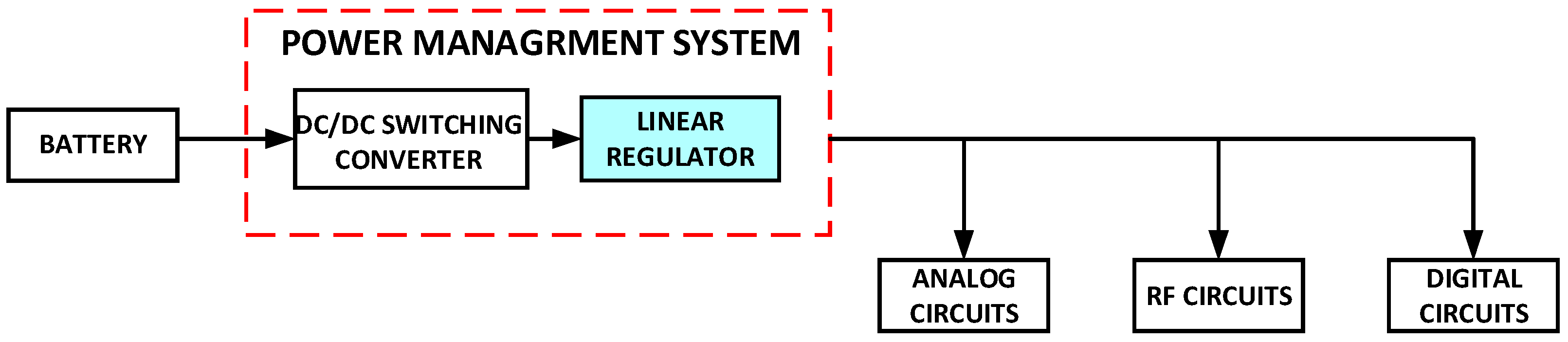
2.1. Overview of Different Categories of Voltage Regulators

A voltage regulator is an integral part of the power management system (PMS) of all electronic devices and it has been the focal point of research over the past few years. The basic block-level architecture of a voltage regulator is shown in Figure 2, which consists of a reference voltage, a feedback network, and a comparator circuit. Figure 2 represents a general block diagram of a voltage regulator.
The voltage sensed at the output terminal is redirected to the comparator circuit through a feedback network that is matched with the reference value set at the comparator. Whenever the comparator circuit discerns any voltage variation, it instantaneously drives the control element to a suitable operating point so as to ensure regulated output voltage. Then, the comparator sends the error signal to the controller, which produces the corrected and regulated output.
Voltage regulators can be divided into two categories, as depicted in Figure 3, in terms of their principle of operation: (1) linear voltage regulator and (2) switching voltage regulator. The main difference between these two categories arises from their pass transistor’s region of operation. The pass element of a linear regulator varies according to the desired level of dropout voltage. When BJT is used as a pass element, the pass element requires high differential value between the input and output. However, when the difference is very low, the pass transistor needs to be operated in an active region to maintain a regulated output. Voltage-controlled FET devices are required to operate in the linear region when large load variation is involved as gate voltage varies according to the load current. On the other hand, FET devices need to set in the saturation region in case the load swing requirement is small. The linear regulator can also be divided into many classes such as a positive adjustable regulator, negative adjustable regulator, floating regulator, and low-dropout (LDO) regulator. However, LDO has become incredibly popular because of its potential and advantages, especially for applications in emerging technologies such as SoC, IoT, and wireless communication. The challenges of LDO designs have pushed researchers to employ novel circuit architectures in different domains such as analog, digital, and hybrid designs to obtain the desired performance trade-off.
Continuous scaling with the inherent benefits of low-cost integration enables the CMOS-based approach to be a competitive platform to implement high-performance electronic devices. Hence, the trend of merging the linear regulator concept with CMOS technology has been apparent over the past few years, considering the wide acceptability of CMOS technology and its superior functioning prospects.

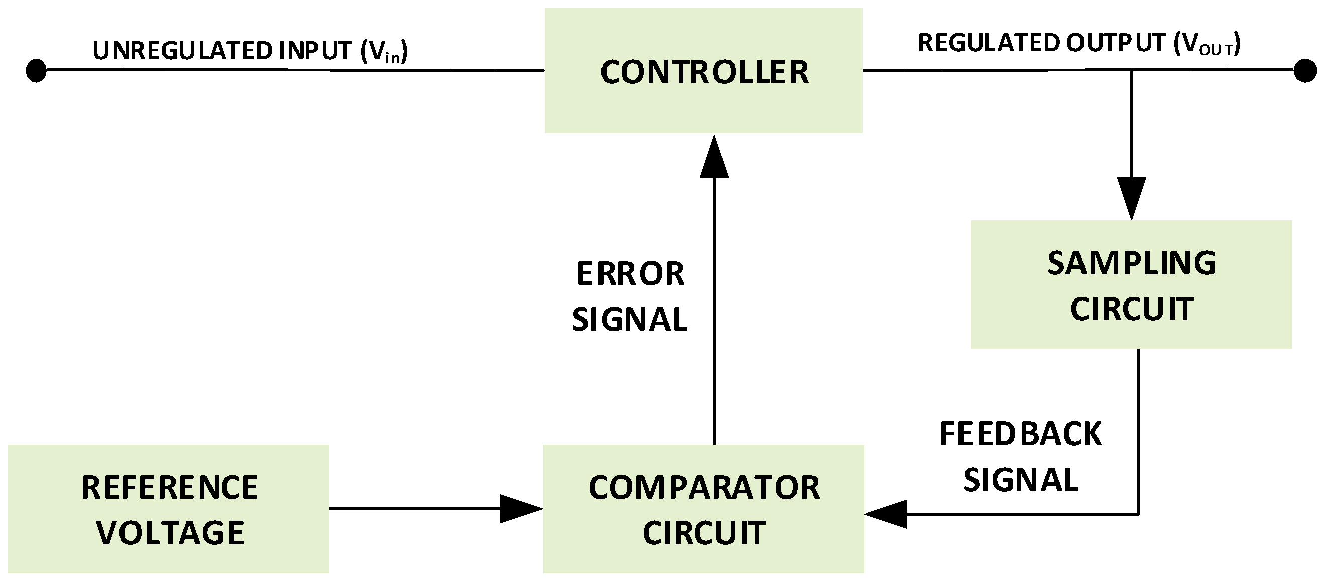
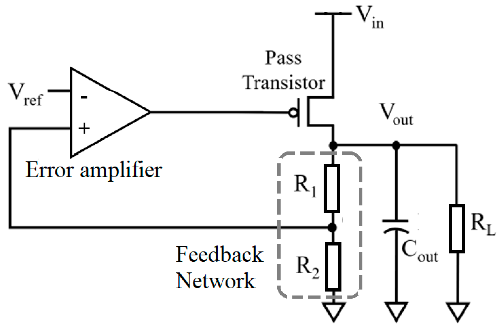
2.2. Linear Regulator Scheme

When the pass transistor of a voltage regulator is operated in the ohmic or linear region, the regulator architecture is known as a linear voltage regulator. The active pass element (such as BJT or MOSFET) of the regulator exploits the linear or saturation region’s characteristics to regulate the output voltage, as shown in Figure 4. Whenever the output diverges from the reference voltage, the current through the pass transistor is varied to obtain the desired output voltage. As a result, the difference between the input and output voltage is dropped in the active pass component, thus, wasting the power through heat dissipation. This type of regulator does not need an extra storage element for transferring energy. This model consumes a smaller area and is free from switching noise. However, it is less efficient than its switching regulator counterpart. Over the decades, the design trends of the linear regulator have evolved from simple series (Figure 4a) or (Figure 4b) shunt structures to several advanced architectures based on its novel topologies such as folded compensation cascode, buffer impedance attenuation, current steering, supercapacitor-assisted, and fast-response adaptive-phase, etc., for different application-specific applications [20,21,22,23,24,25,26,27,28,29,30,31,32,33,34,35,36,37,38,39,40,41,42,43,44,45,46,47,48,49,50,51,52,53,54,55,56,57,58,59,60,61,62,63,64,65].

2.3. Low-Dropout (LDO) Voltage Regulator

As a significant amount of power is dropped in the transistor’s pass element, which reduces the transistor’s voltage drop, this has become a vital issue when designing a linear regulator. The continuous effort of minimizing dropout voltage has developed a new class of linear regulators called low-dropout (LDO) voltage regulators. Generally, when the transistor’s dropout voltage is low, it is considered an efficient LDO voltage regulator in terms of power dissipation. As power dissipation is the product of dropout voltage and load current, the higher dropout voltage indicates that more power will be dissipated as heat. The simple block diagram of LDO, as shown in Figure 5, consists of three main components: the error amplifier, pass transistor, and feedback network. Over the years, different potential techniques have been deployed in each component to meet the desired specification challenges. Several state-of-the-art topologies of LDO design in analog, digital, or hybrid domains are described, respectively, in the following sections.

2.4. LDO Design Parameters

LDO is one of the most fitting linear regulators that is widely accepted in power supply management due to its simplicity, as well as better performance. Following are the most common design parameters of LDO.
Dropout Voltage: Dropout performance is an important parameter when designing a low-dropout linear regulator. The effects of system parameters, dropout performance, and device parameters are interconnected. System parameters have an impact on the LDO’s dropout performance that influences other device parameters. Generally, the summation of the voltage drop across the pass transistor and the output voltage are approximately equal to the input voltage, where the voltage drop is a function of the minimum dropout resistance, RDS, which is the function of the size of the pass element. The error amplifier ensures the desired operating point of the pass transistor so that the output can be maintained at an appropriate level.
Dropout voltage (VDROPOUT) can be defined as the voltage deviation of the output voltage from the input voltage. At dropout voltage, the LDO cannot tune voltage anymore with a further reduction in the input voltage. Mathematically, it can be expressed as the multiplication of load current (ILOAD) and drain-to-source resistance (RDS).
VDROPOUT = ILOAD × RDS
Quiescent Current: Quiescent or ground current (IQ) is the differential current between input and output. It is the minimum current necessary to operate the LDO’s internal circuitry, such as bandgap reference, error amplifier, and output voltage divider when there is no external load current. Several factors such as temperature and topology can affect this value. It can be expressed as
IQ = IINPUTIOUTPUT
Line Regulation: The unit line regulation defines the LDO’s aptness to conserve a specific output voltage (ΔVOUT) against varying input voltage (ΔVIN). It is defined as
LINE REGULATION = ΔVOUTVIN
Load Regulation: Load regulation is a standard used to define the LDO’s capacity to sustain a particular output voltage upon a range of output currents (ΔIOUT) for diverse load conditions. Load regulation is defined as
LOAD REGULATION = ΔVOUTIOUT
Transient Response: The transient response is a measure used to record output voltage variation for a step-change in load current. It depends on several metrics such as slew rate, equivalent series resistance (ESR), and output capacitor
Power Supply Rejection Ratio: Power supply rejection suggests the LDO’s ability to block the swing of the regulated output voltage. PSRR is a dimensionless quantity, whereas PSR is expressed in dB. PSR can be written as
PSRR(dB) = 20log(ΔVIN = ΔVOUT)
PSR(V = V) = ΔV OUT = ΔV IN
Figure of Merit (FOM): The calculation of figure of merit (FOM) is widely adopted by researchers and acts as a collective measure of all other performance parameters. The most established equation for calculating FOM is included in Equation (7), which is adopted by many researchers [19,20,21,22,23,45,47,48,51,52,53,54,55,56,57,58,60,62]. Moreover, several methods of evaluating FOM is presented by authors to signify their design performances, which are added in Equation (8) [25], Equation (9) [44], Equation (10) [58], Equation (11) [59], Equation (12) [51], and Equation (13) [48].
The FOM of capless LDO can also be calculated [62] using Equation (7) where total capacitance is equal to output load capacitance and on-chip capacitance is zero. Moreover, researchers have proposed the FOM equation for comprehending the minimum channel length [48] and output power at which ripple is present [25] to reflect the power consumption and active area performance, while others mentioned those parameters separately. In this review, Equation (7) is considered standard as many researchers utilize it repeatedly. Considering the existing FOM equations, it is apparent that FOM cannot demonstrate the overall performance of LDO in a single quantity; rather, other parameters have to be taken into consideration to fully indicate the performance of an LDO. However, a new computational concept may be proposed integrating other key parameters of LDO design such as fabricated area, power dissipation, and dropout performance that can provide a holistic assessment of the performance of the circuit in a compact form.
F O M   ( s ) = C T O T A L × Δ V O U T × I Q I L m a x 2
Here, C T O T A L is the equivalent capacitance of on-chip capacitance and output load capacitance. Δ V O U T is the differential between voltage measured at minimum load current ( I L m i n ) and voltage measured at maximum load current ( I L m a x ). I L m a x is the maximum load current. I Q is quiescent current.
F O M r i p p l e ( F / A ) = V r i p p l e   × C T P m a x
Here, V r i p p l e   is the output ripple voltage. C T is the total capacitance. P m a x is the output power at which ripple is measured.
F O M   ( V ) = R R × R E × Δ V O U T × I Q Δ I O U T
Here, R R is the settling time ratio, R E is the edge time ratio, Δ I O U T is the difference between the largest and the smallest output current.
F O M   ( s ) = D r o o p   R e c o v e r y   T i m e L o a d   S t e p
F O M   ( H z ) = P o w e r   S u p p l y   R e j e c t i o n × P e a k   P o w e r   E f f i c i e n c y
F O M   ( F ) = C T O T A L × Δ V O U T V O U T   × I Q Δ I L O A D  
Here, V O U T is the output LDO voltage.
F O M   ( V . s ) = T E d g e × Δ V O U T × I Q Δ I L O A D  
Here, T E d g e is the transition time of I L O A D .
Efficiency: The efficiency of an LDO is roughly the ratio of the output voltage to the input voltage (considering negligible IQ) and can be expressed as
EFFICIENCY = IOUT/(IOUT + IQ) × VOUT/VIN × 100%

3. LDO Design Topologies

With the progress of CMOS technology and application-specific metrics’ requirements, the LDO design approach has transfigured significantly over the past few years. This enthralling design scenario has intrigued researchers to improvise their circuit architecture with novel topologies in different domains. A conventional analog LDO (ALDO) with an external capacitor provides good power supply rejection ratio (PSRR) and a transient response. However, it occupies a large area, which usually lessens the system’s reliability. With this pitfall, the designers have approached the capacitorless or “Capless” LDO voltage regulator scheme, which significantly deteriorates the PSSR and transient response performance. Moreover, technology scaling has intrigued researchers to shift their research focus towards the digital domain, which gives rise to a new branch of LDO design called digital LDO (DLDO). However, the switching nature of DLDO produces ripples in output voltage that, in turn, influence PSRR value. Hence, to address the issues mentioned earlier, the designers tried to exploit both ALDO and DLDO together and propose a new hybrid or mixed-mode structured design. Detailed specifications of different performance parameters of reported ALDO, DLDO, and HD-LDO with their respective circuit topologies are appended in Table 1, Table 2 and Table 3, respectively. Although it is hard to compare different types of LDOs, the categorization of discrete LDO architectures can aid researchers for both application-specific and parameter-specific researches on LDO architecture. Figure 6 gives the general classifications of LDO architecture with their offered advantages and disadvantages. In general, it is observed that the ALDO exhibits less ripple in output voltage and offers comparatively better PSSR compared to its DLDO counterpart. On the other hand, the DLDO, mainly, can work with smaller power transistors, has less load dependency, and is more reliable in nature. The HD-LDO (mixed-mode) has the flexibility to adopt the advantages from ALDO and DLDO based on the specifications and requirements of the device.

3.1. ALDO Design Topologies

The fundamental architecture of an ALDO, as illustrated in Figure 7, incorporates a voltage reference, an error amplifier, a feedback network, and a pass transistor. An ALDO has a closed-loop architecture, hence, an efficient feedback design is necessary to maintain stability. Therefore, one of the designer’s goals is to achieve a low quiescent current so that the feedback can operate steadily with high current efficiency. Another design challenge of ALDO is to attain high PSSR with the fast transient response; hence, an additional load capacitor is appended. However, this extra component consumes a large area, which has convinced researchers to model “Capless” ALDO. Moreover, several circuit techniques are amalgamated in other ALDO blocks according to application specifications to improve ALDO’s overall performance, as illustrated below.

3.1.1. Folded Compensation Cascode Topology

A conventional ALDO is demonstrated by Lin et al. (2008) in Figure 8, which implements an active-frequency compensation scheme in order to solve the LDO stability problem [21]. A pseudo-differential technique has been adopted in the frequency compensation circuit with a boosted effective current multiplication factor that generates two similar DC voltages VA and VB, which causes a reduction in the voltage difference at the VA node. An on-chip capacitor, a cascode current-mirror, and a cascode bias current source are employed to reduce the offset current, which, in turn, stabilizes the LDO output voltage. In the proposed design, the supply voltage requirement is minimized by applying folded cascode topology.

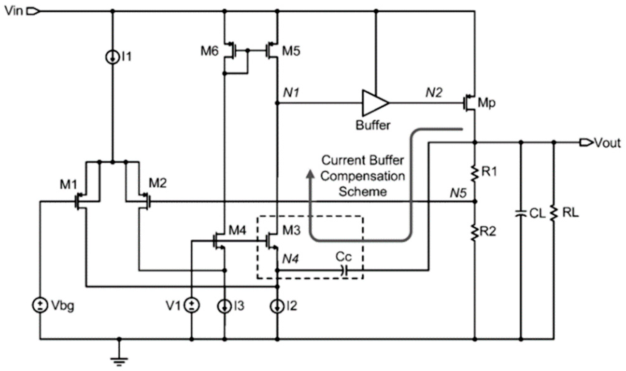
3.1.2. Buffer Impedance Attenuation Topology

M. Al-Shyoukh et al. (2007) proposed a buffer impedance attenuation (BIA) method that drives the pMOS pass device to improve the performance of LDO [22]. Here, dynamically biased shunt feedback causes a reduced output resistance in the buffer, which, in turn, pushes the poles at the gate over the unity gain. Therefore, this process dissipates low-level quiescent current. Figure 9 shows the structure of the LDO implementing the current buffer compensation scheme. The LDO is combined with a bandgap voltage reference of 1V, provided at the error amplifier input. The simple active load connected with the diode generates lower output resistance in comparison with the cascade load that causes the compensation capacitor to lower its value and reach a specific phase margin. Their proposed LDO keeps the error amplifier gain higher than 50dB [22].

3.1.3. Current Steering—Fast Transient LDO

An LDO with a fast transient response is reported by Saberkari et. al. (2013), which utilizes the current steering approach as shown in Figure 10 [23]. A current feedback amplifier (CFA) basically constitutes the control mechanism in the pass transistor. The CFA combines an inverting output buffer and one open-loop voltage follower. The output signal is fed to the CFA along with the feedback network. Therefore, it is contrasted with a reference voltage, and the result is amplified, which controls the pass transistor gate. Fast transient response is obtained through the low impedance at the input of CFA [23].

3.1.4. Current-Mode Feedback Buffer Amplifier-Based LDO

A current-mode feedback buffer amplifier is designed in CMOS 0.25 µm technology to overcome the LDO linear regulator’s common drawbacks, as visualized in Figure 11 [19]. A dual feedback design is implemented where a precise steady-state operation is obtained through global voltage-mode feedback, and fast transient response is received using a current feedback amplifier (CFA) [41]. The design comprises a voltage feedback amplifier (VFA) based on an operational transconductance amplifier (OTA), a second stage CFA, a regulation FET, and a feedback network. The second stage CFA helps in minimizing the settling time of output and reducing the slew rate. On the other hand, accuracy is obtained in a steady-state by the global voltage-mode feedback.

3.1.5. High-Speed Compact Output Driver-Based LDO

A novel architecture of a capacitor-CMOS LDO reported by Saberkari et al. (2013), as shown in Figure 12, used a compact NMOS output driver. The output driver cell generates a low voltage ripple and achieves a fast transient response under large load steps within a minimum chip size [23]. The LDO can generate output voltage as a function of VDD for two different load currents (100 μA and 14 mA). The developed LDO required a 1.8 V of VDD and the LDO’s output voltage follows the input voltage power supply.
The operation of the LDO under dynamic load conditions was simulated using an SoC load model [42]. The power routing digital core of a microcontroller was back-annotated into a schematic view, resulting in an equivalent circuit with a total capacitance of 2.25 nF and 125,000 gates. The load was modeled by using 40% of these gates toggled simultaneously in each clock cycle. The worst-case scenario concerning the microcontroller unit (MCU) operation modes occurs when the MCU is taken from an ultra-low power mode to an active mode when the CPU and all peripheral modules are active [23]. Thus, to simulate the developed LDO under these dynamic conditions, the clock frequency is initially fck = 250 kHz (typical of a low-power mode operation). After 14 μs, the clock frequency is increased to fck = 16 MHz (representing an MCU running in a high-power mode).

3.1.6. Supercapacitor Assisted LDO

Recent developments have led to a wide variety of supercapacitors ranging from fractions of farads to several thousand farads. Simultaneously, the equivalent series resistance (ESR) can vary up to several hundreds of milliohms. Voltage ratings of supercapacitor modules can exceed 100V, whereas the single-cell devices reach about 4.0 V [24]. Applications include memory backups, surge absorption, wind energy, and portable devices [13,24].
A simple variation of the supercapacitor topology [24] is shown in Figure 13. Figure 13a demonstrates the first phase where the input voltage of the LDO drops to the lowest value Vin(min) during the charging period of the supercapacitor. In the next step, the supercapacitor and input of LDO are connected in parallel to losing the stored energy, displayed in Figure 13b.

3.1.7. Fast-Response Adaptive-Phase LDO

The 65nm CMOS technology was used to design an improved DC–DC converter with a fast-response adaptive-phase (fast-RAP) digital controller [25]. Compared to cascaded linear regulators, fast-RAP controllers have a quicker response rate, and, thus, these controllers will maintain a good transient response. This design is capable of enhancing line and load regulations of the charge pump and can develop efficient standalone linear regulators. Without the need for further step-ups, this method can lower dropout voltage, as displayed in Figure 14. In the presence of a high load transient, all the phases are activated simultaneously. A clock tripler is also required to maintain the transient response while assisting in the implementation of an adaptive-phase scheme [25].

3.1.8. Feedforward Compensated High-Voltage Linear Regulator LDO

A unique framework of the linear regulator with high current sinking potential targeting the capacitive micromachined ultrasonic transducer (CMUT) technology [43]. The regulator embodies a high voltage NMOS pass transistor, feedback network, an error amplifier, and a biasing resistor, depicted in Figure 15. The feedback network consists of two high voltage N-doped poly resistors utilized to intuit any anomaly in output voltage. Furthermore, the transistor’s channel length and width are adjusted in such a way that provides minimal resistivity to subside gate capacitance.

3.1.9. High Power Supply Rejection Linear Regulator LDO

A design proposed by Chen et al. (2020) provides several appealing features, including high power supply rejection (PSR), wideband ripple filtering, and fast transient response [44], as shown in Figure 16. The linear voltage regulator of the design incorporates four blocks: (1) an N-type pass transistor, (2) output-supplied voltage reference circuit, (3) charge pump, and (4) dual feedback system. Bypassing the usage of a voluminous decoupling capacitor is considered one of the fascinating aspects of this design, while the shortfall of decoupling capacitance is tackled by a two-stage feedback structure comprised of a high-gain and a wide-bandwidth path. Additionally, a deep N-well NMOS is employed to cope with the fluctuating output voltage, which escalates the breakdown voltage to 2.8V from 1.8V and neutralizes the body effect.

3.1.10. Concurrent Bulk Modulation and Forward Body Bias

An innovative structure for a low-dropout (LDO) regulator suitable for the sub-1-V supply [45] is demonstrated in Figure 17. The primary blocks of this design are a common-source-configured PMOS, rail-to-rail error amplifier (EA), buffer (BUF), and load current generator (LCG). The adaptive biasing technique, efficient forward body biasing (FBB), modified driving concept, and novel concurrent bulk modulation approach enables this design to accomplish the desired characteristics. In this design, the buffer is engineered based on a differential flipped voltage follower (FVF) that demonstrates approximately zero voltage shifting from input to output. Additionally, LCG provides the required bias current to maintain the loop stability when the load current is zero.

3.1.11. Current-Mode Feedforward Ripple Canceller

A linear low-dropout regulator, as illustrated in Figure 18, is reported by Joshi et al. (2020) adopting a current-mode feedforward ripple canceller (CFFRC) in order to facilitate high power supply rejection (PSR), fast load transient response, and low quiescent current, simultaneously [46]. The LDO architecture integrates the PMOS power FET, power FET driver buffer, folded cascade error amplifier (EA), CFFRC amplifier, and compensation network. The benefits of both the feedforward and the current-mode technique are optimized in a single circuit. The feedforward approach is convenient to maintain low quiescent power consumption and reduce noise by adjusting the impedance ratio. The current-mode is chosen over the voltage-mode due to its inherent ability to improve PSR without the cost of padding extra circuit elements.

3.1.12. Negative Charge Pump-Enhanced (NCPE) LDO

The analog LDO depicted in Figure 19 was implemented especially for low-voltage applications [47], ensuring a balance between the power supply and the efficiency. The amplification is performed in two distinct stages: the error amplifier (EA) stage and the gain stage. The negative charge pump’s output is linked with the ground terminal of both amplifiers. The power transistor is powered by the outcome of the gain stage amplifier, which increases load regulation. As the NCP is not connected directly with the power transistor, it cancels the possibility of adding ripples.

3.1.13. Low-VDD Inverting Buffer with Efficient Feedforward Path

An LDO design by Park et al. (2020), as illustrated in Figure 20, uses a low-VDD inverting buffer and an efficient feedforward path to produce a high-performance inverting buffer with additional transistors and capacitors [48]. Though it consumes extra area compared to the traditional buffer circuits, it eliminates the pole-effect, hence upgrading the PSSR performance of LDO. Moreover, the feedforward path is engineered as such by replacing constant current sources with dynamic current sources. This approach allows the output signal to bypass the high impedance node, thus improving stability.

3.1.14. Multistage Error Amplifier and PRDTRA-Based LDO

An LDO design especially for low-power SoC applications has been demonstrated by Huang et al. (2020), as shown in Figure 21 [49]. The idiosyncrasies of this architecture are a multistage error amplifier (EA) accompanied by the transient acceleration pulse generator (TAPG) and a feedback network optimized by a programmable recursively divide by two resistor array (PRDTRA). The error amplifier contains three successive stages: the main gain stage, the gain-boosting stage, and the output stage. The common-mode rejection ratio (CMRR) of the output stage cancels the power noises transmitted through the previous two steps. A TAPG also follows the output stage to provide an additional route to enlarge the transient response. Moreover, the circuit optimizes the PRDTRA algorithm to achieve the scaling of the output voltage.

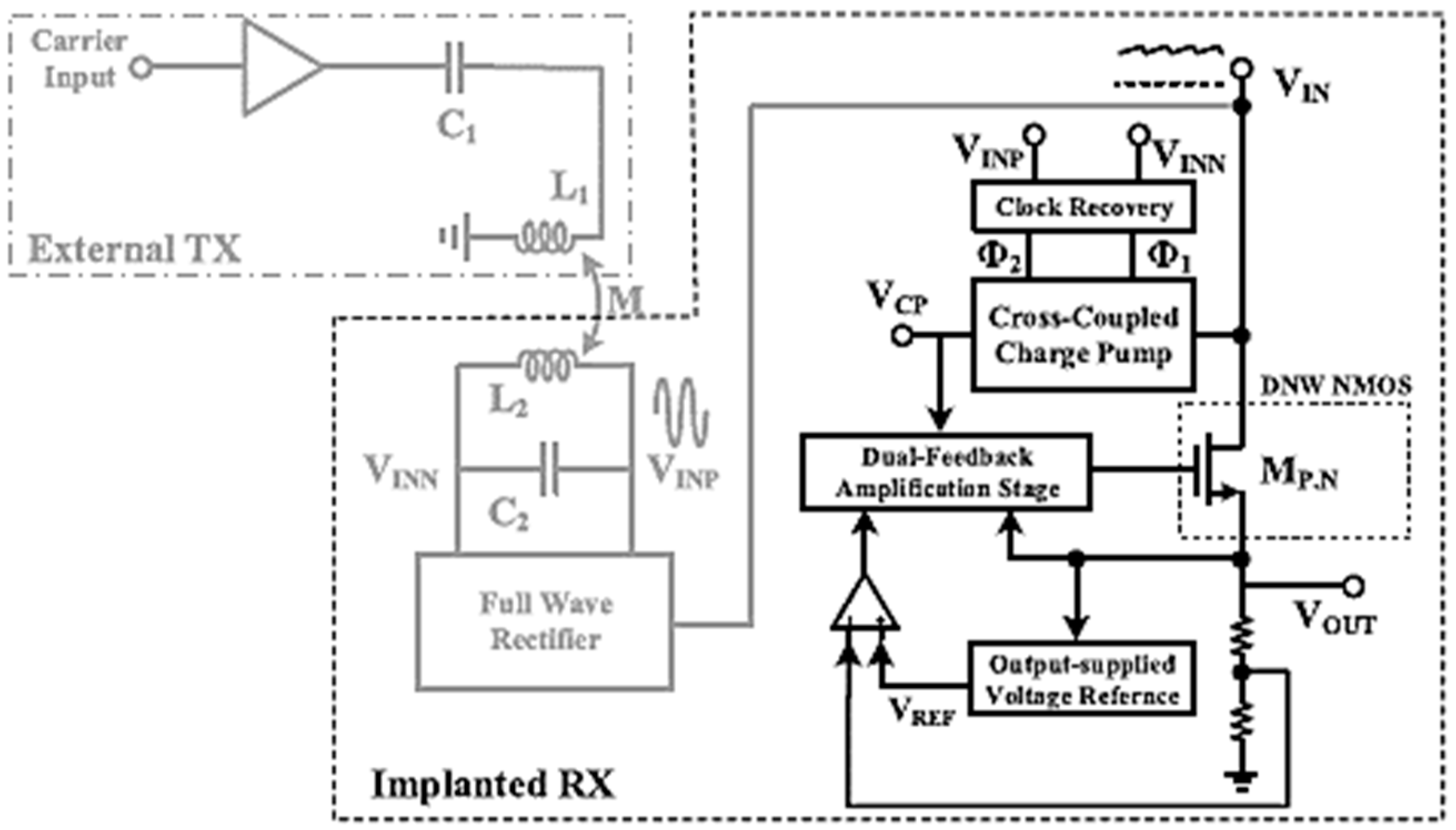
3.1.15. Switched RC Bandgap Reference LDO

A low-noise LDO circuit implemented for noise-sensitive mixed-signal applications is shown in Figure 22 [50]. The LDO circuit is vulnerable to various noises such as thermal noise, shot noise, flicker noise, etc. A sample and hold switched RC filter eliminates the noises produced by the bandgap reference circuit and scaling amplifier before entering the error amplifier. The flicker noise generated by the two-stage error amplifier is filtered using the drain-side modulated current-mode chopping technique. The ripples created at the EA are suppressed by a switched capacitor (SC) notch filter. Furthermore, a first-order passive RC filter is also introduced to cancel the noise in the bias circuit.

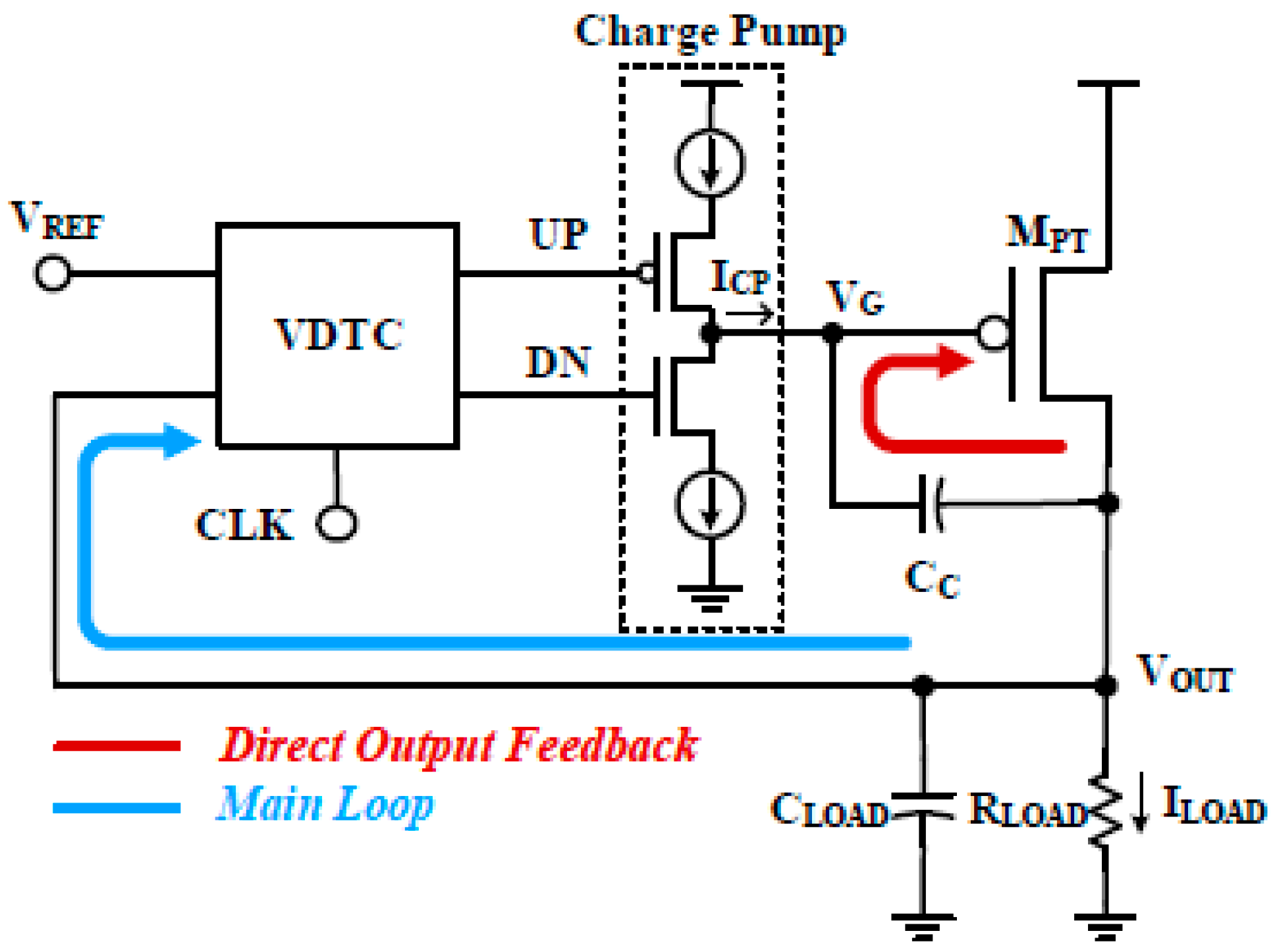
3.1.16. Voltage Difference to Time Converter with Direct Output Feedback

A low-dropout regulator scheme modeled based on a voltage difference to time converter (VDTC) was reported by Shin et al. (2020), as given in Figure 23 [51]. Extracting attributes from both digital and analog LDOs, the design yields a ripple-free output and small quiescent current over a broad range of operating voltage. The structure contains a VDTC, a power transistor, a charge pump, and a coupling capacitor. The VDTC performs the role of sensing the difference between the reference and the output voltage, and the result is updated in every clock cycle. Moreover, the load current can be adjusted quickly during rapid transition through an optimized direct output feedback loop.

3.1.17. Performance Comparison of ALDO

Table 1 reflects the comparative analysis of several ALDO architectures with respect to their performance metrics. The data listed in the table signify the design flexibility of ALDO according to the application-specific considerations. Among several designs, the best LDO performance in terms of maximum allowable current conveyed is 600 mA [48], which is a significant improvement as it allows a current value almost three times larger than the second-best Imax value reported [22]. Recent advances in ALDO design prefer capless architecture because of its acceptability in fully on-chip implementation as well as economical considerations. In the aforementioned table, some designs offer capacitorless architecture [48,50], whereas one design has the lowest output capacitor requirement (0.05 µF) [19] compared to others. Quiescent current is another important parameter of LDO design as it expresses the minimum current requirement of the internal circuitry of LDO. Therefore, the smaller the quiescent current, the better the LDO design. The necessary quiescent current is the minimum value, which is only 0.016 µA [45]. One design offers the minimum low-dropout voltage along with the maximum current efficiency [51]. There are a few other parameters such as dropout voltage and current efficiency that define the overall performance of LDO.
Table 1 also indicates the various kinds of circuit topology with respect to various designs where the important parameters of the specific circuit structures can be identified. The design in [48] supports the maximum load current and incorporates the concept of a low-VDD inverting buffer with the cost of an additional transistor and replacing the constant current source with a dynamic current source. Thus, it allows the output signal to avoid a high impedance path and improves the current value. Both the capacitorless architecture and architecture with capacitors have their advantages and disadvantages. Because of the off-chip capacitor, there remains a dominant pole at the output that ensures a good load and line regulation with better stability. However, the capacitor performance may degrade at a high frequency because of effective series inductance (ESR) and effective series resistance (ESR). On the other hand, capless architecture, a tempting choice for SoC applications, lessens the number of external pins and metal bonds, sacrificing the stable output pole. Design [50] achieves a capless architecture by improvising a low-pole passive RC filtering circuit in the bandgap reference (BGR) circuit to eliminate the noises created by the BGR circuit. The other capless design [48], introduces an efficient buffer circuit that alleviates the pole-up effect at a higher frequency, thus relaxing the necessity for an off-chip capacitor. Design [45] presents an optimized rail-to-rail buffer utilizing a differential flipped voltage follower (DFVF), which cancels out the use of an auxiliary amplifier for bulk modulation, thus limiting the quiescent current. In addition, there are several circuit techniques such as the current feedback amplifier, buffer impedance attenuation, folded cascode topology, dual feedback structure with charge pump, and multistage error amplifier with TAPG that are prominent in ALDO design. The objective of design [47] is to establish an LDO architecture that can be operated in a low voltage domain to enhance battery life. Therefore, the designer introduced a negative charge pump in the controller section to extend the voltage range of the error amplifier. Similarly, the design in [51] achieved a target of low voltage operation by using a different technique of a voltage to time converter with direct output feedback. On the other hand, the focus of design [49] was to achieve clean power by suppressing ripples, which is accomplished by adapting the concept of the multistage error amplifier. The linear regulator proposed in reference [43] is designed for a capacitive micromachined ultrasonic transducer (CMUT), where the driver circuit should switch between two discrete high-level voltages. The linear regulator designed in [43] is suitable for this kind of application, which reduces the additional circuit requirement similar to a level-shifter. Moreover, the input and output voltages of LDO proposed in reference [23] are 3–5 V and 2.8 V. Thus, the calculated dropout voltage is 200–2200 mV, which is capable of regulating a large voltage range. The LDO designs presented in [23,43] are for special applications only and are rarely considered as references for ALDO design.

3.2. DLDO Design Topologies

With the expansion of System-on-Chip (SoC) applications, the power management system requires LDO suitable for low-voltage operation. This scenario has drawn scholars to attempt to devise LDO in the digital domain. The basic model of DLDO contains a voltage reference, comparator, a digital controller, and an array of pass transistors. The switching nature of the DLDO transistor generates a significant amount of output ripple, thus degrading PSSR characteristics. Therefore, the primary concern of the DLDO design is to minimize the ripples. Furthermore, several approaches are employed in the controller part to avoid unnecessary operations to accomplish a fast response. Figure 24 illustrates the basic architecture of a conventional DLDO [52].

3.2.1. Proportional Derivative (PD) Compensation and Sub-LSB Duty Control

An unprecedented design approach for a recursive digital low-dropout regulator (RDLDO), shown in Figure 25, demonstrates the potential for an optimal response time and improved load regulation range compared with the previous design [53]. This design utilizes a successive approximation (SAR) algorithm, Sub-LSB pulse width modulation (PWM) duty control technique, and proportional derivative (PD) compensation scheme to ensure a befitting substitution of analog LDOs. An efficient PD compensation configuration swiftly discerns the output voltage, which stamps out the overshoots and undershoots during SAR transformation and maintains stability. Sub-LSB PWM control brings forth gate voltage information that alleviates the DC accuracy limitation and output voltage peak-to-peak ripple limitation.

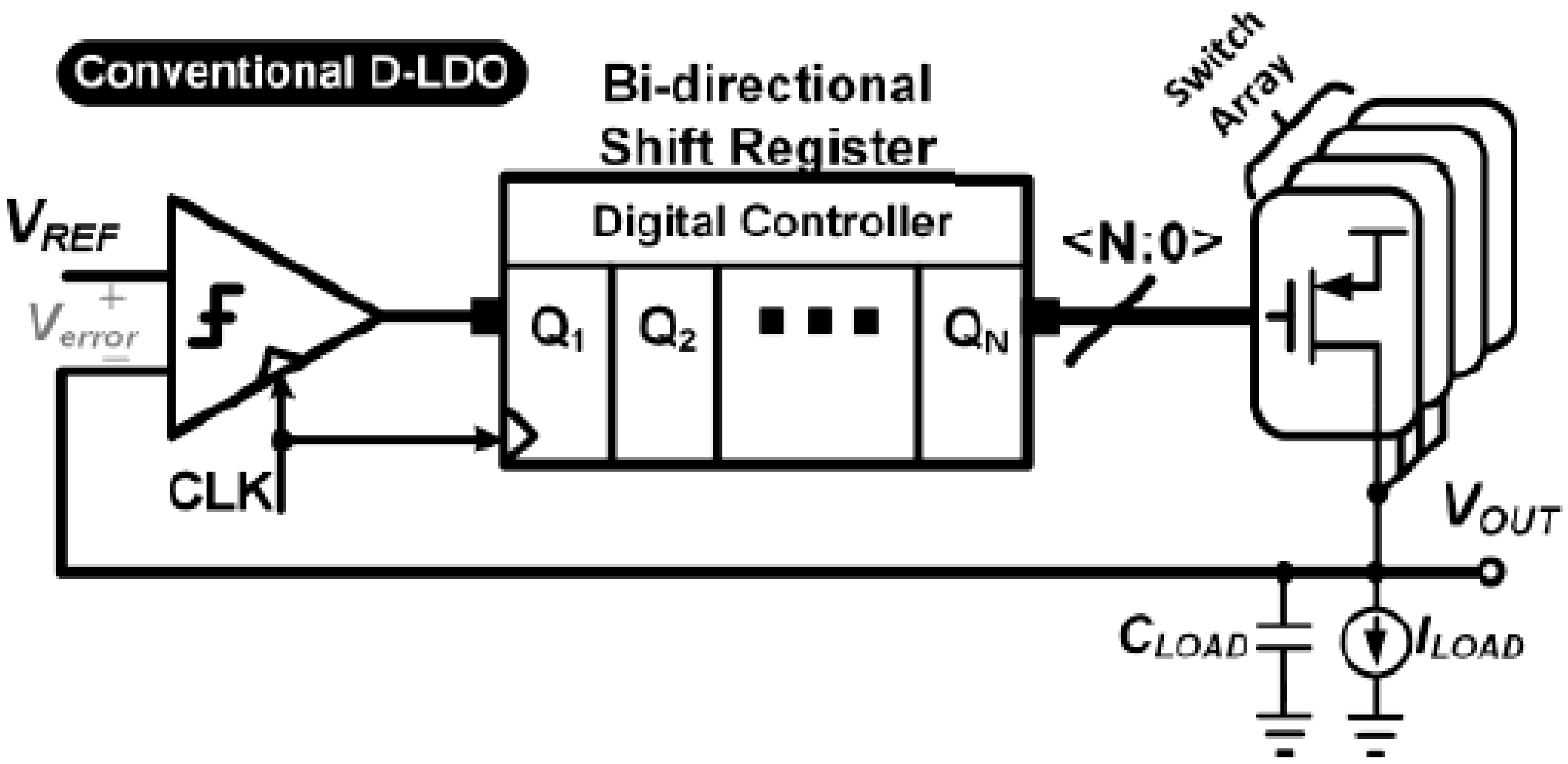
3.2.2. Fully Standard Cell-Based Digital LDO

With the evolution of CMOS technology, digital low-dropout (DLDO) regulators are continuously becoming popular among researchers because of their near-threshold voltage operation potentials. A standard cell-based DLDO regulator offers a small quiescent current and fast load transient response, as depicted in Figure 26 [52]. This design’s fundamental components are a logic threshold-triggered comparator (LTTC), multi-mode detector, multi-loop switchable controller, and 12-bit binary-segmented MOS. The CMOS inverter-based LTTC keeps track of the difference between the reference and output voltage. The multi-mode controller section consists of three sub-sections: fixed-gain accumulator (FG-ACC), variable-gain accumulator (VG-ACC), and successive approximation register (SAR). Finally, the circuit achieves 99.97% current efficiency, which is the prime concern of a conventional DLDO design.

3.2.3. Coarse–Fine Dual Loop Digital LDO

Figure 27 shows a digital low-dropout (LDO) regulator suitable for mobile application processors (MAP). The two loops, such as a coarse loop and fine loop are used to control the output voltage [54]. Both loops have certain aspects in terms of performance parameters. For instance, the coarse loop utilizes a speedy current-mirror flash analog to digital converter (ADC), which provides a large output current and improves transient performance. The fine loop minimizes the ripples in voltage while supplying a low-level output current.

3.2.4. Event-Driven Explicit Time-Coding Architecture-Based DLDO

Load current handling is a prime concern when designing a low-dropout voltage regulator. To manipulate the rapid fluctuation of the load current, a traditional DLDO optimizes a high-frequency clock; however, this impacts the power efficiency and the transient response of the LDO. An event-driven strategy is utilized to address this issue in the design, as illustrated in Figure 28 [55], which avoids irrelevant operations by responding to a new event. The proposed architecture contains four primary blocks: a 3-bit continuous-time ADC, trigger generator, proportional-integral (PI) controller, and power transistor. Whenever a deviation from the seven pre-defined reference voltages is spotted, the trigger generator immediately delivers a signal to the PI controller. The PI controller’s response decides the operation of the power transistor, thus controlling the required quantity of current to the load.

3.2.5. Beat-Frequency Quantizer and VCO-Based DLDO

A digital LDO using a beat-frequency (BF) quantizer, as shown in Figure 29, was introduced instead of a classic voltage quantizer [56]. The overall architecture of the DLDO comprises four components: a voltage-controlled oscillator, time quantizer, digital controller, and pass transistor. The proposed BF time quantizer is designed efficiently to adjust the sampling frequency according to the change in the operation mode (steady-state, overshoot). Adaptive voltage positioning (AVP) is exploited to cope with the voltage change and ensure good regulation and transient response performance.

3.2.6. Time-to-Digital Converter (TDC)-Based DLDO

A time-to-digital converter (TDC)-based DLDO was implemented to upgrade the transient response, as shown in Figure 30 [57]. The proposed DLDO comprises three primary blocks: a TDC-based signal converter, digital controller, and PMOS array. Here, the time-to-digital converter (TDC) is preceded by a voltage sensor, which records the capacitor’s charging time, thus achieving high linearity. Furthermore, this model’s controller section is engineered using a digital PI controller rather than a conventional shift register, which allows for multi-bit operation in a single clock cycle; hence, it improves the transient response.

3.2.7. Performance Comparison of DLDO

Table 2 indicates the performance summary for the DLDO design parameters of the linear regulator schemes from previous researchers. FOM is a key criterion in evaluating the performance of CMOS linear regulators. The lower the FOM, the better the design. Packaging parasitic inductances, gate driving loss, and switching loss are some of the critical factors playing a role in regulating the FOM. Therefore, when the device is operating at a comparatively low frequency, FOM is good for evaluating materials and acts as a performance parameter in optimization. The lowest FOM of 1.11 ps was achieved by the design in [55] in the year 2017. The performance of FOM increases by the quiescent current over the maximum load current due to the time response of the processor. A lower FOM ensures an improved transient response. In this design, the researchers accomplished superior performance of the overall DLDO design by integrating several efficient modules such as a 3-bit continuous-time ADC, trigger generator, PI controller, and power transistor. The design in [53] shows the best result in terms of area consumption, occupying only 0.0023 mm2. Again, design [52] shows the best output in terms of low quiescent current and maximum current efficiency. Here, the designer maneuvered a logic threshold-triggered comparator instead of a conventional comparator triggered by the clock frequency. Thus, the design reduces the current consumption and maximizes the current efficiency. Among several tabulated designs, the top architecture in terms of the off-chip capacitor is proposed by [56], requiring only 40 pF. In this design, the sampling frequency of the bit frequency quantizer responds with the voltage droop, hence, the successive clock edge comes faster. Due to this adaptive sampling technique, instead of fixed sampling, the circuit needs a low load capacitor. The maximum load current is achieved by design [54] as the flash analog to digital converter of this design consumes only static current. In addition, the prime concern of design [57] was to improve the transient response by replacing the traditional single-bit conversion technique with a multi-bit conversion technique. For this, the designer proposed a voltage sensor-based time-to-digital converter (TDC), which removes the reliance on the buffer gate’s delay time to operate the TDC.

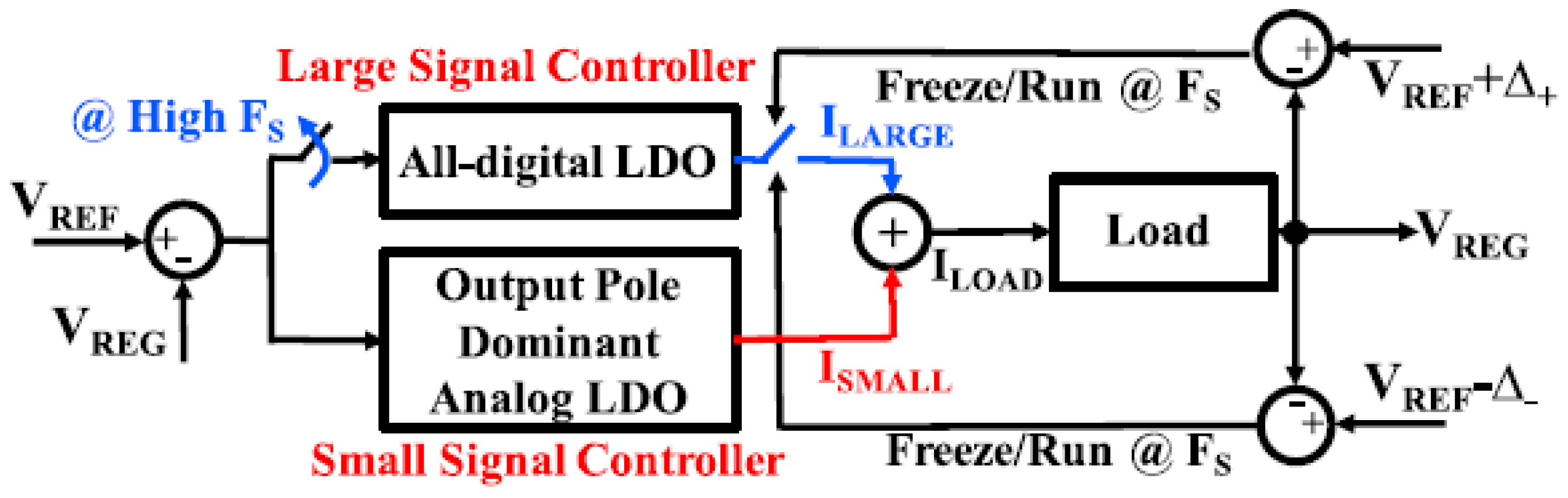
3.3. HD-LDO Design Topologies

The prime drawbacks of ALDOs are their ability to control large transient currents, though they display better performance in terms of small signal regulation. Contrastingly, DLDOs exhibit accurate large signal performance, however, their overall performance degrades due to clocking and dynamic power consumption. Considering the amalgamation of both analog and digital loads and the necessity of discrete operating ranges in the same platform, designers have been required to merge the features of both ALDO and DLDO. Therefore, the mixed-mode LDO could employ the advantages of multiple power rails in the chip, and split the high-efficiency power conversion task through a low-dropout digital voltage rail, and achieve a satisfactory noise rejection capability through a high-dropout voltage rail. The basic architecture of the hybrid LDO is shown in Figure 31, which has an ALDO in parallel with a DLDO [58]. The DLDO branch undertakes the 80–90% majority of the LDO current with a coarse granularity power train. The quantization error of the coarse granularity is absorbed by the ALDO branch. Selected recent state-of-the-art works of the hybrid LDO design are described in the following section.

3.3.1. Scan Reconfigurable Hybrid LDO

A hybrid low-dropout (LDO) voltage regulator [59] operates in four distinct modes, as illustrated in Figure 32. The design exploits both analog and digital LDO with discrete current sources that allow the flexibility to select desired power efficiency and power supply noise rejection (PSR) standards upon choosing a specific operation mode. For example, mode-1 exhibits high power efficiency with low PSR, whereas mode-3 displays high PSR with low power efficiency.

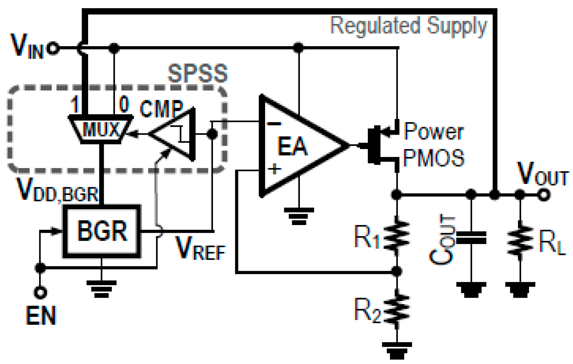
3.3.2. Bandgap Reference-Based Hybrid LDO

Power supply rejection (PSR) performance is a crucial design parameter of LDO due to its ability to smoothen output voltage by suppressing ripples [60]. The bandgap-based LDO, as depicted in Figure 33, offers several benefits such as high power supply rejection (PSR), variable frequency range, finite ripple rejection, low design intricacy, low power consumption, swift transient response, and high stability. The multiplexer decides that either the input or output voltage will be linked with the bandgap reference supply-rail (BGR). As this architecture utilizes the output voltage rather than the noisy input voltage to the PSR of BGR, it ensures excellent PSR of LDO even if the ripple rejection of BGR is not commendable.

3.3.3. Active Ripple Suppression-Based HD-LDO

A hybrid LDO structure combining a DLDO and an analog ripple cancellation amplifier (RCA) [61] is illustrated in Figure 34. A DLDO and RCA are operated in parallel to ensure swift and stable operation, mitigating voltage ripples. A DLDO is prone to quantization error due to its switching nature; therefore, the RCA is operated along with the DLDO to counterbalance this error. The DLDO structure is also efficiently devised, incorporating analog to digital converter (ADC) feedback, a PID controller, and a current-mode digital to analog converter (DAC).

3.3.4. Switched-Mode-Control-Based Hybrid LDO

A hybrid LDO design based on switched-mode-control (SMC), shown in Figure 35, is made suitable for less power-consuming applications [58]. The design combines an all-digital LDO with an output pole dominant analog LDO to extract advantages from both domains. To perform instant switching, SMC is proposed, which comprises a large signal (LS) and a small signal (SS) controller. A voltage-based error signal decides which controller will be used. Thus, this design achieves fine-grain power management, a fast response, and an efficient regulation scheme.

3.3.5. Exponential-Ratio Array (ERA)-Based Hybrid LDO

A capacitorless hybrid LDO incorporating a thermometer-coded exponential-ratio array (ERA) [63] produced a weak-gain ALDO, depicted in Figure 36. The analog and the digital loop of the HLDO work in parallel to ensure stability, eliminating the necessity of an extra capacitor. The ERA lessens the required number of bits and PMOS transistors, thus widening the load current range and allowing a fast transient response. Moreover, an augmented linear proportional controller (ALPC) improves the linearity of digital loop tracking.

3.3.6. Performance Comparison of HD-LDO

DLDO architectures are highly desirable because of the increasing number of digital loads and decent large signal transient performance, etc. Nevertheless, DLDO suffers from output ripple, whereas ALDO performs better small signal regulation with suppressed ripple. In face of the above consideration, researchers are intrigued by the idea of using the hybrid LDO strategy of the linear voltage regulator as it extracts features from both the digital and the analog domains of LDOs. The HD-LDO is the most attractive design due to its multi-domain conglomerate design availability according to application specifications. However, in search of achieving the desired performance, HD-LDO requires additional and complex circuitry. The performances of several parameters of different types of LDOs are tabulated in Table 3. Among several designs, [63] presents the superior peak current efficiency with 99.7% performance along with low quiescent current and capless architecture. It also shows better performance in terms of FOM compared to other designs’ available data. The designer utilized a 255-bit thermometer-coded exceptional-ratio array (ERA), which reduces the tracking time and suppresses the voltage drop, thus improving the current efficiency. The loop stability is generated by digital logic as the system clock is operated at a much slower speed than settling time. Moreover, the output PMOS in the digital loop can produce an output dominant pole, therefore, moving towards a capless architecture. Furthermore, another unique feature of design [62] is its wide load current range. Again, the maximum load current is achieved in design [60], which is almost thrice the relevant best possible data [61]. Design [60] shows a good power supply rejection ratio (PSRR), which is not tabulated in Table 3. The novelty of this design lies in the implementation of additional feedforward ripple cancellation techniques and a modified gate buffer. Both the capacitorless design [61,63] and design with output capacitors [58,59] are observed in the HD-LDO design. Moreover, the focus of design [59] is to achieve a broad range of PSSR to generate clean power. Some other parameters are also enlisted in the table, but they are not compared due to the lack of available data.

4. Conclusions

This article reviewed the linear regulators in CMOS technology developed by previous researchers. There are many aspects used to identify the performance of the circuit such as the dropout performance, FOM, percentage of current efficiency, power consumption, die area, etc. The study aimed to provide some ideas of possible method modifications to increase the current efficiency and performance of linear regulators. The current efficiency greatly impacts the stability of the circuit in low load current conditions. Dropout voltage affects PSRR, power consumption, and noise performance. FOM signifies the combined impacts of various parameters such as on-chip capacitance, maximum load, output voltage swings, etc. Researches discussed in this paper put significant effort into improving the LDO performance, ranging from application-specific feature development to the trade-off between several specifications. This documentation, as a handy framework, can benefit upcoming researches regarding LDO architectures. The illustrative designs and detailed comparisons presented in this paper can assist researchers to have a better understanding of current developments and promote further improvements in linear regulator circuit designs.

Author Contributions

Methodology, K.J.A.O., investigation, M.R.H., formal analysis, K.N.M. and M.S.K.H.; writing—original draft preparation, O.M.D. and M.R.H.; writing—review and editing, M.A.S.B., M.B.I.R. and F.H.; supervision, M.B.I.R. All authors have read and agreed to the published version of the manuscript.

Funding

The authors acknowledge the support of the grant FRGS/1/2020/TK0/XMU/02/5 from the Ministry of Higher Education (MoHE), Malaysia, the grant XMUMRF/2020-C6/IECE/0017 and XMUMRF/2021-C8/IECE/0021 from Xiamen University Malaysia and the grant GUP-2021-019 from Universiti Kebangsaan Malaysia.

Institutional Review Board Statement

Not Applicable.

Informed Consent Statement

Not Applicable.

Data Availability Statement

Not Applicable.

Conflicts of Interest

The authors declare no conflict of interest.

References

  1. Badal, T.I.; Reaz, M.B.I.; Bhuiyan, M.A.S.; Kamal, N. CMOS Transmitters for 2.4-GHz RF Devices: Design Architectures of the 2.4-GHz CMOS Transmitter for RF Devices. IEEE Microw. Mag. 2019, 20, 38–61. [Google Scholar] [CrossRef]
  2. Bhuiyan, M.A.S.; Badal, M.T.I.; Reaz, M.B.I.; Crespo, M.L.; Cicuttin, A. Design Architectures of the CMOS Power Amplifier for 2.4 GHz ISM Band Applications: An Overview. Electronics 2019, 8, 477. [Google Scholar] [CrossRef] [Green Version]
  3. Badal, M.T.I.; Reaz, M.B.I.; Jalil, Z.; Bhuiyan, M.A.S. Low power high-efficiency shift register using implicit pulse-triggered flip-flop in 130 nm CMOS process for a cryptographic RFID tag. Electronics 2016, 5, 92. [Google Scholar] [CrossRef] [Green Version]
  4. Folla, J.K.; Wembe, E.T.; Essimbi, B.Z.; Crespo, M.L.; Cicuttin, A.; Reaz, M.B.I.; Bhuiyan, M.A.S. An 8.72 µW low-noise and wide bandwidth FEE design for high-throughput pixel-strip (PS) sensors. Sensors 2021, 21, 1760. [Google Scholar] [CrossRef]
  5. Folla, J.K.; Crespo, M.L.; Wembe, E.T.; Bhuiyan, M.A.S.; Cicuttin, A.; Essimbi, B.Z.; Reaz, M.B.I. A low-offset low-power and high-speed dynamic latch comparator with a preamplifier-enhanced stage. IET Circuits Devices Syst. 2021, 15, 65–77. [Google Scholar] [CrossRef]
  6. Bhuiyan, M.A.S.; Reaz, M.B.I.; Jalil, J.; Rahman, L.F.; Chang, T.G. A compact transmit/receive switch for 2.4 GHz reader-less active RFID tag transceiver. J. Cent. South Univ. 2015, 22, 546–551. [Google Scholar] [CrossRef]
  7. Sood, L.; Agarwal, A. A CMOS standard-cell based fully-synthesizable low-dropout regulator for ultra-low power applications. Int. J. Electron. Commun. 2021, 141, 153958. [Google Scholar] [CrossRef]
  8. Manikandan, P.; Bindu, B. A transient enhanced cap-less low-dropout regulator for wide range of load currents and capacitances. Microelectron. J. 2021, 115, 105207. [Google Scholar] [CrossRef]
  9. Badal, T.I.; Reaz, M.B.I.; Yeng, L.S.; Bhuiyan, M.A.S.; Haque, F. Advancement of CMOS transimpedance amplifier for optical receiver. Trans. Electr. Electron. Mater. 2019, 20, 73–84. [Google Scholar] [CrossRef]
  10. Boanloo, M.M.; Yavari, M. A low-power high-gain low-dropout regulator for implantable biomedical applications. Circuits Syst. Signal Process. 2021, 40, 1041–1060. [Google Scholar] [CrossRef]
  11. Sun, Q.; Zhang, Y.; Guo, C.H.; Jaaskelainen, K.; Hu, Y. A fully integrated CMOS voltage regulator for supply-noise-insensitive charge pump PLL design. Microelectron. J. 2010, 41, 240–246. [Google Scholar] [CrossRef]
  12. Tseng, C.Y.; Wang, L.W.; Huang, P.C. An integrated linear regulator with fast output voltage transition for dual-supply SRAMs in DVFS systems. IEEE J. Solid-State Circuits 2010, 45, 2239–2249. [Google Scholar] [CrossRef]
  13. Maity, A.; Patra, A. Trade-offs Aware Design Procedure for an Adaptively Biased, Capacitor-less Low Drop-out Regulator Using Nested Miller Compensation. IEEE Trans. Power Electron. 2016, 31, 369–380. [Google Scholar] [CrossRef]
  14. Mustafa, N.B.; Amin, S.; Reaz, M.B.I.; Hashim, F.H.; Kamal, N. Evolution of low drop out voltage regulator in CMOS technologies. Prz. Elektrotech. 2015, 91, 26–33. [Google Scholar] [CrossRef] [Green Version]
  15. Zhang, Y.; Ma, D. A fast-response hybrid SIMO power converter with adaptive current compensation and minimized cross-regulation. IEEE J. Solid-State Circuits 2014, 49, 1242–1255. [Google Scholar] [CrossRef]
  16. Walling, J.S.; Allstot, D.J. Linearizing CMOS switching power amplifier using supply regulator. IEEE Trans. Circuit Syst. 2010, 57, 497–501. [Google Scholar] [CrossRef]
  17. Zhang, H.; Dower, P.M. A max-plus based fundamental solution for a class of discrete time linear regulator problems. Linear Algebra Appl. 2015, 471, 693–729. [Google Scholar] [CrossRef] [Green Version]
  18. Park, B.; Kim, J.; Cho, Y.; Jin, S.; Kang, D.; Kim, B. CMOS linear power amplifier with envelope tracking operation. J. Electromagn. Eng. Sci. 2014, 14, 1–8. [Google Scholar] [CrossRef] [Green Version]
  19. Oh, W.; Bakkaloglu, B. A CMOS low-dropout regulator with current-mode. IEEE Trans. Circuits Syst. II Express Briefs 2007, 54, 922–926. [Google Scholar] [CrossRef]
  20. Priewasser, R.; Agostinelli, M.; Unterrieder, C.; Marsili, S.; Hueme, M. Control and implementation of DC-DC converters for variable frequency operation. IEEE Trans. Power Electron. 2014, 29, 287–301. [Google Scholar] [CrossRef]
  21. Lin, H.C.; Wu, H.H.; Chang, T.Y. An active-frequency compensation scheme for CMOS low-dropout regulators with transient-response improvement. IEEE Trans. Circuits Syst. II Express Briefs 2008, 55, 853–857. [Google Scholar] [CrossRef]
  22. Shyoukh, M.A.; Lee, H.; Perez, R. A transient-enhanced low-quiescent current low-dropout regulator with buffer impedance attenuation. IEEE J. Solid-State Circuits 2007, 42, 1732–1741. [Google Scholar] [CrossRef] [Green Version]
  23. Saberkari, A.; Alarcón, E.; Shokouhi, S.B. Fast transient current-steering CMOS LDO regulator based on current feedback amplifier. Integration 2013, 46, 165–171. [Google Scholar] [CrossRef]
  24. Kankanamge, K.; Kularatna, N. Improving the end-to-end efficiency of DC–DC converters based on a supercapacitor-assisted low-dropout regulator technique. IEEE Trans. Ind. Electron. 2014, 61, 223–230. [Google Scholar] [CrossRef]
  25. Lu, Y.; Ki, W.; Yue, C.P. An NMOS-LDO regulated switched-capacitor DC-DC converter with fast-response adaptive-phase digital control. IEEE Trans. Power Electron. 2016, 31, 1294–1303. [Google Scholar] [CrossRef]
  26. Hazucha, P.; Moon, S.T.; Schrom, G.; Paillet, F.; Gardner, D.; Rajapandian, S.; Karnik, T. High voltage tolerant linear regulator with fast digital control for biasing of integrated DC-DC converters. IEEE J. Solid-State Circuits 2007, 42, 66–73. [Google Scholar] [CrossRef]
  27. Yang, Y.; Chun, H.; Torsten, L. Dual-stacked current recycling linear regulators with 48% power saving for biomedical implants. IEEE Trans. Circuits Syst. I Regul. Pap. 2013, 60, 1946–1958. [Google Scholar] [CrossRef]
  28. Guo, J.; Leung, K.N. A 6W chip-area-efficient output-capacitorless LDO in 90-nm CMOS technology. IEEE J. Solid-State Circuits 2010, 45, 1896–1905. [Google Scholar] [CrossRef]
  29. Hazucha, P.; Karnik, T.; Bloechel, B.A.; Parsons, C.; Finan, D.; Borkar, S. An area-efficient, integrated, linear regulator with ultra-fast load regulation. IEEE J. Solid-State Circuits 2005, 40, 933–939. [Google Scholar] [CrossRef]
  30. Man, T.Y.; Leung, K.N.; Leung, C.Y.; Mok, P.K.T.; Chan, M. Development of single-transistor-control LDO based on flipped voltage follower for SoC. IEEE Trans. Circuits Syst. I Regul. Pap. 2008, 55, 1392–1401. [Google Scholar] [CrossRef] [Green Version]
  31. Chong, S.; Chan, P.K. A 0.9-/spl mu/A quiescent current output-capacitorless LDO regulator with adaptive power transistors in 65-nm CMOS. IEEE Trans. Circuits Syst. I Regul. Pap. 2013, 60, 1072–1081. [Google Scholar] [CrossRef]
  32. Li, S.; Zhao, X.; Dong, L.; Yu, L.; Wang, Y. Design of a capacitor-less adaptively biased low dropout regulator using recycling folded cascode amplifier. Int. J. Electron. Commun. 2021, 135, 153745. [Google Scholar] [CrossRef]
  33. Asif, M.; Ali, I.; Khan, D.; Rehman, M.R.; Pu, Y.; Yoo, S.S.; Lee, K.Y. Design of high performance hybrid type digital-feedback low drop-out regulator using SSCG technique. IEEE Access 2021, 9, 28167–28176. [Google Scholar] [CrossRef]
  34. Li, J.; Li, J.; Zhang, J.; Xu, Q.; Qu, P.; Hu, W.; Xiao, Z. An adaptively biased LDO regulator with 11nA quiescent current and 50mA available load. In Proceedings of the 2021 IEEE International Symposium on Circuits and Systems (ISCAS), Daegu, Korea, 22–28 May 2021; pp. 1–5. [Google Scholar] [CrossRef]
  35. Yang, H.C.; Huang, M.H.; Chen, K.H. High-PSR-bandwidth capacitor-free LDO regulator with 50µA minimized load current requirement for achieving high efficiency at light loads. WSEAS Trans. Circuits Syst. Arch. 2008, 7, 428–437. Available online: http://www.wseas.us/e-library/transactions/circuits/2008/30-815N.pdf (accessed on 29 October 2021).
  36. Chen, J.; Zhang, W.; Sun, Q.; Liu, L. An 8–12.5-GHz LC PLL with dual VCO and noise-reduced LDO regulator for multilane multiprotocol SerDes in 28-nm CMOS technology. Electronics 2021, 10, 1686. [Google Scholar] [CrossRef]
  37. Bahramali, A.; Lopez-Vallejo, M. An RFID-based self-biased 40 nm low power LDO regulator for IoT applications. Micromachines 2021, 12, 396. [Google Scholar] [CrossRef] [PubMed]
  38. Song, Y.; Oh, J.; Cho, S.Y.; Jeong, D.K.; Park, J.E. A fast droop-recovery event-driven digital LDO with adaptive linear/binary two-step search for voltage regulation in advanced memory. IEEE Trans. Power Electron. 2021, 37, 1189–1194. [Google Scholar] [CrossRef]
  39. Lu, Y.; Ki, W.H. Linear Regulators for WPT. In CMOS Integrated Circuit Design for Wireless Power Transfer; Analog Circuits and Signal Processing; Springer: Singapore, 2018. [Google Scholar] [CrossRef]
  40. Aziz, F.I.B.A.; Mamun, M.; Bhuiyan, M.A.S.; Bakar, A.A.A. A low drop-out voltage regulator in 0.18 µm CMOS technology. Mod. Appl. Sci. 2013, 7, 70–76. [Google Scholar] [CrossRef]
  41. Crepaldi, P.C.; Pimenta, T.C.; Moreno, R.L.; Rodriguez, E.C. A low power CMOS voltage regulator for a wireless blood pressure biosensor. IEEE Trans. Instrum. Meas. 2012, 61, 729–739. [Google Scholar] [CrossRef]
  42. Boas, A.V.; Haddad, S.P.; Dias, J.A.S. A CMOS fast transient response low-dropout regulator with a compact NMOS output driver. Microelectron. J. 2014, 45, 272–276. [Google Scholar] [CrossRef]
  43. Sakolski, O.; Poongodan, P.K.; Vanselow, F. A feedforward compensated high-voltage linear regulator with fast response, high-current sinking capability. IEEE Solid-States Circuits Lett. 2020, 3, 114–117. [Google Scholar] [CrossRef]
  44. Chen, Y.P.; Tang, K.T. A fully integrated high-power-supply-rejection linear regulator with an output-supplied voltage reference. IEEE Trans. Circuits Syst. I Regul. Pap. 2020, 67, 3828–3838. [Google Scholar] [CrossRef]
  45. Adorni, N.; Stanzione, S.; Boni, A. A 10-mA LDO with 16-nA IQ and operating from 800-mV supply. IEEE J. Solid-State Circuits 2020, 55, 404–413. [Google Scholar] [CrossRef]
  46. Joshi, K.; Manandhar, S.; Bakkaloglu, B. A 5.6 µA wide bandwidth, high power supply rejection linear low-dropout regulator with 68 dB of PSR up to 2 MHz. IEEE J. Solid-State Circuits 2020, 55, 2151–2160. [Google Scholar] [CrossRef]
  47. Tan, Y.; Zhan, C.; Wang, G. A fully-on-chip analog low-dropout regulator with negative charge pump for low-voltage applications. IEEE Trans. Circuits Syst. II Express Briefs 2018, 66, 1361–1365. [Google Scholar] [CrossRef]
  48. Park, J.; Lee, B.; Hong, S.W. A output capacitor-less low-dropout regulator with a low-VDD inverting buffer for the mobile application. IEEE Trans. Ind. Electron. 2020, 67, 8931–8935. [Google Scholar] [CrossRef]
  49. Huang, C.H.; Liao, W.C. A high-performance LDO regulator enabling low-power SoC with voltage scaling approaches. IEEE Trans. Very Large Scale Integr. Syst. 2020, 28, 1141–1149. [Google Scholar] [CrossRef]
  50. Magod, R.; Suda, N.; Ivanov, V.; Balasingam, R.; Bakkalogu, B. A low noise output capacitor-less low dropout regulator with a switched-RC bandgap reference. IEEE Trans. Power Electron. 2017, 32, 2856–2864. [Google Scholar] [CrossRef]
  51. Shin, K.; Jee, D.W.; Jeon, D. A 65nm-.6-1.2V low-dropout regulator using voltage-difference-to-time converter with direct output feedback. IEEE Trans. Circuits Syst. II Express Briefs 2020, 68, 67–71. [Google Scholar] [CrossRef]
  52. Akram, M.A.; Hong, W.; Hwang, I.C. Fast transient fully standard-cell-based all digital low-dropout regulator with 99.97% current efficiency. IEEE Trans. Power Electron. 2018, 33, 8011–8019. [Google Scholar] [CrossRef]
  53. Salem, L.G.; Warchall, J.; Mercier, P.P. A successive approximation recursive digital low-dropout voltage regulator with PD compensation and sub-LSB duty control. IEEE J. Solid-State Circuits 2018, 53, 35–49. [Google Scholar] [CrossRef]
  54. Lee, Y.J.; Qu, W.; Singh, S.; Kim, D.Y.; Kim, K.H.; Kim, S.H.; Park, J.J.; Cho, G.H. A 200-mA digital low drop-out regulator with coarse_fine dual loop in mobile application processor. IEEE J. Solid-State Circuits 2017, 52, 64–76. [Google Scholar] [CrossRef]
  55. Kim, D.; Seok, M. A fully integrated digital low-dropout regulator based on event-driven explicit time-coding architecture. IEEE J. Solid-State Circuits 2017, 52, 3071–3080. [Google Scholar] [CrossRef]
  56. Kundu, S.; Liu, M.; Wen, S.J.; Wong, R.; Kim, C.H. A fully integrated digital LDO with bulit-in adaptive sampling and active voltage positioning using a beat-frequency quantizer. IEEE J. Solid-State Circuits 2019, 54, 109–120. [Google Scholar] [CrossRef]
  57. Zhang, H.; Wan, P.; Geng, J.; Liu, Z.; Chen, Z. a fast transient response digital LDO with a TDC-based signal converter. Electronics 2020, 9, 132. [Google Scholar] [CrossRef] [Green Version]
  58. Nasir, S.B.; Sen, S.; Raychowdhury, A. switched-mode-control based hybrid LDO for fine-grain power management of digital load circuits. IEEE J. Solid-State Circuits 2018, 53, 569–581. [Google Scholar] [CrossRef]
  59. Nasir, S.B.; Sen, S.; Raychowdhury, A. A reconfigurable hybrid low dropout voltage regulator for wide-range power supply noise rejection and energy-efficiency trade-off. IEEE Trans. Circuits Syst. II Express Briefs 2018, 65, 1864–1868. [Google Scholar] [CrossRef]
  60. Kim, D.K.; Shin, S.U.; Kim, H.S. A BGR-recursive low-dropout regulator achieving high PSR in the low-to mid-frequency range. IEEE Trans. Power Electron. 2020, 35, 13441–13454. [Google Scholar] [CrossRef]
  61. Cheah, M.; Mandal, D.; Bakkaloglu, B.; Kiaei, S. A 100-mA, 99.11% current efficiency 2-m Vpp ripple digitally controlled LDO with active ripple suppression. IEEE Trans. Very Large Scale Integr. Syst. 2017, 25, 696–704. [Google Scholar] [CrossRef]
  62. Zhang, Y.; Song, H.; Zhou, R.; Rhee, W.; Shim, I.; Wang, Z. A capacitor-less ripple-less hybrid LDO with exponential ratio array and 4000x load current range. IEEE Trans. Circuits Syst. II Express Briefs 2019, 66, 36–40. [Google Scholar] [CrossRef]
  63. Kayıhan, H.İ.; İnam, B.B.; Doğan, B.; Yelten, M.B. A wide-temperature range (77–400 K) CMOS low-dropout voltage regulator system. Analog. Integr. Circuits Signal Process. 2021, 106, 501–510. [Google Scholar] [CrossRef]
  64. Bailón, J.P.; Calvo, B.; Medrano, N. A fully-integrated 180 nm CMOS 1.2 V low-dropout regulator for low-power portable applications. Electronics 2021, 10, 2108. [Google Scholar] [CrossRef]
  65. Kuang, J.J.; Liang, H.; Zhang, J.; Qin, Y.; Zhang, Z.W.; Wang, Z.; Zhang, B. A fast-transient low-dropout regulator with current-efficient super transconductance cell and dynamic reference control. IEEE Trans. Circuits Syst. I Regul. Pap. 2021, 68, 2354–2367. [Google Scholar] [CrossRef]
Figure 1. Voltage Regulator in a Power Management System.
Electronics 11 00193 g001
Figure 2. The Block Diagram of a Voltage Regulator.
Electronics 11 00193 g002
Figure 3. Classification of Voltage Regulator.
Electronics 11 00193 g003
Figure 4. Block Diagram of (a) Series Linear Regulator (b) Shunt Linear Regulator.
Electronics 11 00193 g004
Figure 5. Basic Block Diagram of LDO Voltage Regulator.
Electronics 11 00193 g005
Figure 6. Characteristics of different types of LDOs.
Electronics 11 00193 g006
Figure 7. The basic structure of a conventional ALDO [40].
Electronics 11 00193 g007
Figure 8. The basic structure of a conventional ALDO [40].
Electronics 11 00193 g008
Figure 9. Structure of the LDO using the current buffer compensation scheme [22].
Electronics 11 00193 g009
Figure 10. LDO architecture based on CFA [23].
Electronics 11 00193 g010
Figure 11. LDO architecture using CFA-based buffer amplifier [19].
Electronics 11 00193 g011
Figure 12. The LDO with compact output driver [23].
Electronics 11 00193 g012
Figure 13. Concept of supercapacitor energy recovery: (a) minimizing the series element dissipation; (b) reuse of stored energy in the supercapacitor [24].
Electronics 11 00193 g013
Figure 14. Block diagram of the fully integrated regulated switched capacitor dc–dc converter with fast-RAP control [25].
Electronics 11 00193 g014
Figure 15. Feedforward Compensated High-Voltage Linear Regulator [43].
Electronics 11 00193 g015
Figure 16. High PSR linear regulator [44].
Electronics 11 00193 g016
Figure 17. Concurrent Bulk Modulation and FBB-Based ALDO [45].
Electronics 11 00193 g017
Figure 18. Current-mode FFRC-based ALDO [46].
Electronics 11 00193 g018
Figure 19. Negative Charge Pump-Enhanced ALDO [47].
Electronics 11 00193 g019
Figure 20. Low-VDD Inverting Buffer-based ALDO [48].
Electronics 11 00193 g020
Figure 21. Multistage EA and PRDTRA-Based LDO [49].
Electronics 11 00193 g021
Figure 22. Switched RC Bandgap Reference ALDO [50].
Electronics 11 00193 g022
Figure 23. VDTC-Based ALDO [51].
Electronics 11 00193 g023
Figure 24. Basic Structure of Conventional DLDO [52].
Electronics 11 00193 g024
Figure 25. The architecture of PD Compensation and Sub-LSB Duty Control DLDO [53].
Electronics 11 00193 g025
Figure 26. Fully Standard Cell-Based DLDO [52].
Electronics 11 00193 g026
Figure 27. Coarse–Fine Dual Loop-Based DLDO [54].
Electronics 11 00193 g027
Figure 28. Event-Driven Explicit Time-Coding DLDO [55].
Electronics 11 00193 g028
Figure 29. Beat-Frequency Quantizer and VCO-Based DLDO [56].
Electronics 11 00193 g029
Figure 30. Time-to-Digital Converter (TDC)-based DLDO [57].
Electronics 11 00193 g030
Figure 31. Basic Architecture of HD-LDO [58].
Electronics 11 00193 g031
Figure 32. The architecture of Scan Reconfigurable Hybrid LDO [59].
Electronics 11 00193 g032
Figure 33. Bandgap Reference-based Hybrid LDO [60].
Electronics 11 00193 g033
Figure 34. Active Ripple Suppression-based HD-LDO [61].
Electronics 11 00193 g034
Figure 35. Switched-Mode-Control-based HD-LDO [58].
Electronics 11 00193 g035
Figure 36. Exponential-Ratio Array (ERA)-based HD-LDO [62].
Electronics 11 00193 g036
Table 1. Summary of the ALDO performance comparison.
ReferencesProcess
(µm)
Imax
(mA)
Vin
(V)
Vout
(V)
Cout
(µF)
IQ
(µA)
Δ V O U T
(mV)
V D R O P
(mV)
Load reg. (mV/mA)Line reg. (mV/V)Current Efficiency (%)Active Area (mm2)PSR
(dB)
TopologyFOM #
(ps)
[19]0.25502–2.51.5–1.970.051000.475300.08N/A99.80.2343 @ 30 KHzCurrent Feedback Amplifier940
[22]0.352002.01.81.0200.220034299.80.264340 @ ILMBuffer Impedance Attenuation100
[21]0.351502.01.81.0270.2200100600.40940 @ 20 KHzFolded Cascade Topology0.01
[23]0.351003–52.8159–189322000.02513.599.8N/A>56 (0 Hz–100 Hz)Current Steering Approach17.7
[25]0.65302.513910195500.2080.30.1542.8 @ 100 mHzAdaptive Phase Scheme0.085 and 0.08 n *
[50]0.25100N/A1–3.3Capless40N/A230N/AN/AN/A0.2150 @ 10 KHzSample and Hold Switched RC FilterN/A
[47]0.065450.60.510−421441000.047199.950.045N/ANegative Charge Pump0.1037
[44]0.18111.31.09N/A276452100.0150.6N/A0.105−54 @ 10 MHzDual Feedback Structure with Charge Pump10.49
and
0.677 mV **
[43]0.18070660.0662880.1740001.79099.710.15N/AFeedforward Compensated Method0.03
[45]0.055100.80.610.016702001.050.5N/A0.04242.7 @ 50 KHzDifferential Flipped Voltage Follower11.4
[49]0.041001.1–1.90.2–1.1156289000.1760.85799.940.375−60 @ 1 MHzMultistage Error Amplifier with TAPG157
[48]0.56001.5–5.01.3–4.85.1 × 10−616.55142000.0110.15699.950.082−26.7 @ 1 MHzLow-VDD Inverting Buffer0.00012 and 1.42 ns.mV ***
[51]0.65600.6–1.20.5–1.1510−50.1–10111100N/AN/A99.990.086N/AVoltage Difference to Time Converter0.000202 and 0.182 fF ****
# All FOM values are calculated using Equation (7). * FOM is calculated using Equation (8). ** FOM is calculated using Equation (9). *** FOM is calculated using Equation (13). **** FOM is calculated using Equation (12).
Table 2. Summary of the DLDO performance comparison.
References[54][52][55][56][53][57]
Technology (nm)286565656565
VIN (V)1.10.7–1.20.5–10.6–1.20.5–10.7–1.1
VOUT (V)0.90.6–1.10.45–0.950.4–1.10.3–0.450.65–1.05
VOUT (mV) @ ILOAD (mA)120@180[email protected][email protected]108@50[email protected]371@80
ILOAD,MAX (mA)200250.0072–3.5111002120
IQ (mA)0.20.0060.012–0.2160.1–1.070.0140.495
Current Peak Efficiency (%)99.9499.9796.399.599.899.6
CLOAD (nF)23.510.40.040.40.5
Load Regulation (mV/mA)N/A0.04N/A0.638<5.60.6
Line Regulation (mV/V)N/A0.78N/AN/A2.30.5
PSRR (dB)N/AN/AN/A–38@1MHzN/AN/A
Active Area (mm2)0.0210.0140.0290.03740.00230.017
Response Time, TR (ns)N/AN/AN/AN/A15.12.1
FOM #7.75 (ps)2.17 (ps)1.11 (ps)1.38 (ps)199 (ps)8.7 (ps)
Circuit TopologyCurrent-mirror flash analog to digital converter (ADC)Logic-Threshold Triggered ComparatorEvent-Driven Explicit Time-CodingBeat-Frequency Quantizer and VCOPD Compensation and Sub-LSB Duty ControlTime-to-Digital Converter (TDC)
# All FOM values are calculated using Equation (7).
Table 3. Summary of the HD-LDO performance comparison.
References[61][58][59][63][60]
Technology (nm)18013013065500
Input Voltage, VIN (V)1.43–2.00.6, 1.1–1.2N/A0.8–1.02.2–5
Output Voltage, VOUT (V)1.0–1.570.5–0.55, 0.8–1.1N/A0.75–0.952–4.85
VDROP (mV)N/AN/AN/A50120 (P-type)
Maximum ILOAD (mA)1001250.01–40300
Quiescent Current, IQ (mA)1N/A0.0570.120.050
Current Peak Efficiency (%)99.1198.5 (R), 98.64 (L)98.8699.7N/A
COUT(nF)Cap-Free0.50.5Cap-Free1
Load Regulation (mV/mA)0.01<2.67N/AN/A0.003
Line Regulation (mV/V)1N/AN/AN/A0.28
PSR (dB)N/AN/A−9 to −34 @ 100 MHzN/A80 @0.1 MHz
Active Area (mm2)0.6790.0818N/A0.175N/A
FOM (ps) #N/A166(R), 244.8 (Linear)
and 0.58 (R), 1.747(Linear) ns/mA ##
28.06
and 28.06 @
100 MHz ###
0.018811
# All FOM values are calculated using Equation (7). ## FOM values are calculated using Equation (10). ### FOM values are calculated using Equation (11).
Publisher’s Note: MDPI stays neutral with regard to jurisdictional claims in published maps and institutional affiliations.

