Article

Digital Image Blending Using Inaccurate Addition

by
Padmanabhan Balasubramanian
1,
Raunaq Nayar
2 and
Douglas L. Maskell
1,*
1
School of Computer Science and Engineering, Nanyang Technological University, 50 Nanyang Avenue, Singapore 639798, Singapore
2
Transport Research Centre, College of Engineering, Nanyang Technological University, 50 Nanyang Avenue, Singapore 639798, Singapore
*
Author to whom correspondence should be addressed.
Electronics 2022, 11(19), 3095; https://doi.org/10.3390/electronics11193095
Submission received: 7 July 2022 / Revised: 20 September 2022 / Accepted: 23 September 2022 / Published: 28 September 2022

Abstract

:
Inaccurate computing is found to be a high-speed, low-power and energy-efficient alternative to accurate computing for error-tolerant applications. In this context, this paper analyzes the usefulness of inaccurate computing for a digital image processing application, viz. digital image blending, which has been less explored. We analyze the use of inaccurate addition for image blending used in applications such as photo editing and computer graphics. For experimentation, we considered blending two digital images using accurate and inaccurate addition separately. We considered many inaccurate addition architectures which are suitable for implementation in both FPGA and ASIC design environments to perform a comparative analysis. We found that an inaccurate addition with an optimum inaccuracy produces a similar quality of blended image as obtained using accurate addition. The quality of blended images is quantified using standard metrics such as the peak signal-to-noise ratio and the structural similarity index measure. In particular, an inaccurate adder, M-HERLOA, was found to be preferable for image blending from the combined perspectives of quality of blended image, error metrics and design metrics. We implemented the accurate and inaccurate adders corresponding to an optimum inaccuracy in FPGA and ASIC design environments. We considered a Xilinx Artix-7 FPGA for an FPGA-based implementation and a 32/28 nm CMOS standard digital cell library for an ASIC type standard cell-based implementation. The results show that, for an FPGA-based implementation, M-HERLOA enables a reduction in delay by 13%, requires 50% fewer LUTs and 49% fewer registers and consumes 24.3% less on-chip power compared to the accurate high-speed FPGA adder while yielding a blended image of good quality. For an ASIC type standard cell-based implementation, M-HERLOA enables a reduction in delay by 64.6% (24.4%), requires 43% (82.4%), less area and dissipates 63% (67.8%) less power than the accurate carry ripple adder (carry look-ahead adder).

1. Introduction

Inaccurate computing is a high-speed, low power and energy-efficient alternative to accurate computing for error-tolerant practical applications [1,2]. Examples of such applications include digital signal processing [3,4,5], multimedia [6], big data and analytics [7], neuromorphic computing [8], hardware implementation of neural networks for AI and machine learning [9], software engineering [10], memory storage [11], memory systems for multicore processors [12], low power graphics processing [13], etc. Inaccurate computing is realized using inaccurate hardware and/or software and/or memory storage. In this paper, we consider using inaccurate hardware for an image blending application that has been relatively less explored. In specific, we consider the use of inaccurate adders and compare their performance with the accurate adder for a digital image blending application to analyze their usefulness and determine an optimum circuit from the perspectives of output quality, error metrics, and design metrics.
Inaccurate adders can be broadly categorized into static inaccurate adders and dynamic inaccurate adders. A static inaccurate adder [3] incorporates a fixed inaccuracy by reducing the logic of an accurate adder and so it tends to guarantee savings in the design metrics (i.e., area, delay, and power) compared to an accurate adder when physically implemented. Static inaccurate adders produce deterministic sum outputs which may or may not be accurate depending upon the input supplied and the adders’ architecture. The extent of inaccuracy that can be incorporated in a static inaccurate adder is best estimated based on prior knowledge of the inherent error resiliency of a target application. Another approach may be to analyze the error tolerance of an application by trial and error and then determine the optimum inaccuracy that can be incorporated in a static inaccurate adder for use in a specific application. A dynamic inaccurate adder [14] is different from a static inaccurate adder in that it can generate accurate or inaccurate sum outputs on demand depending upon the extent of inaccuracy that can be tolerated by a specific application. This is typically made possible by including an error detection and correction logic as part of a dynamic inaccurate adder. Error detection and correction circuit help to tune the output of a dynamic inaccurate adder to meet a specified accuracy range but the error detection and correction circuit form a design overhead. Moreover, depending upon the architecture of a dynamic inaccurate adder, configuring its output to satisfy a prescribed accuracy range may necessitate multiple computation (i.e., clock) cycles. Hence, the choice of an inaccurate adder for a practical application should weigh the pros and cons of static and dynamic inaccurate adders. In [5], for a digital video encoding application, it was noted that the savings in power achieved by a dynamic inaccurate adder are comparable with a static inaccurate adder.
Static inaccurate adders, in turn, can be classified into three types based on their implementation method—the first type relates to full-custom, i.e., transistor-level ASIC type implementation [3,4,15,16,17], the second type corresponds to FPGA-based implementation [18,19,20] and the third type is suitable for semi-custom i.e., gate-level (standard cell based) ASIC type implementation and also FPGA based implementation [21,22,23,24,25,26,27,28,29,30,31,32,33,34,35,36]. Given this, the third type of static inaccurate adders is versatile as they can be implemented in both FPGA and ASIC design environments and, in this work, we consider the architectures of the third type of static inaccurate adders. Henceforth, in the following discussions, by ‘inaccurate adder’ we refer to a ‘static inaccurate adder’ unless stated otherwise.
In the rest of this paper, Section 2 gives the acronyms of various approximate adders along with their expansions for quick reference. Section 3 describes the architectures of various inaccurate adders, which are suitable for implementation in FPGA and ASIC design environments. Section 4 discusses the image blending application and shows blended images obtained using the accurate adder and inaccurate adders corresponding to an optimum inaccuracy. Section 5 presents the error characteristics of inaccurate adders and their calculated error parameters corresponding to an optimum inaccuracy. Section 6 presents the design metrics of accurate and inaccurate adders corresponding to FPGA and ASIC type implementations. Section 7 finally concludes the paper.

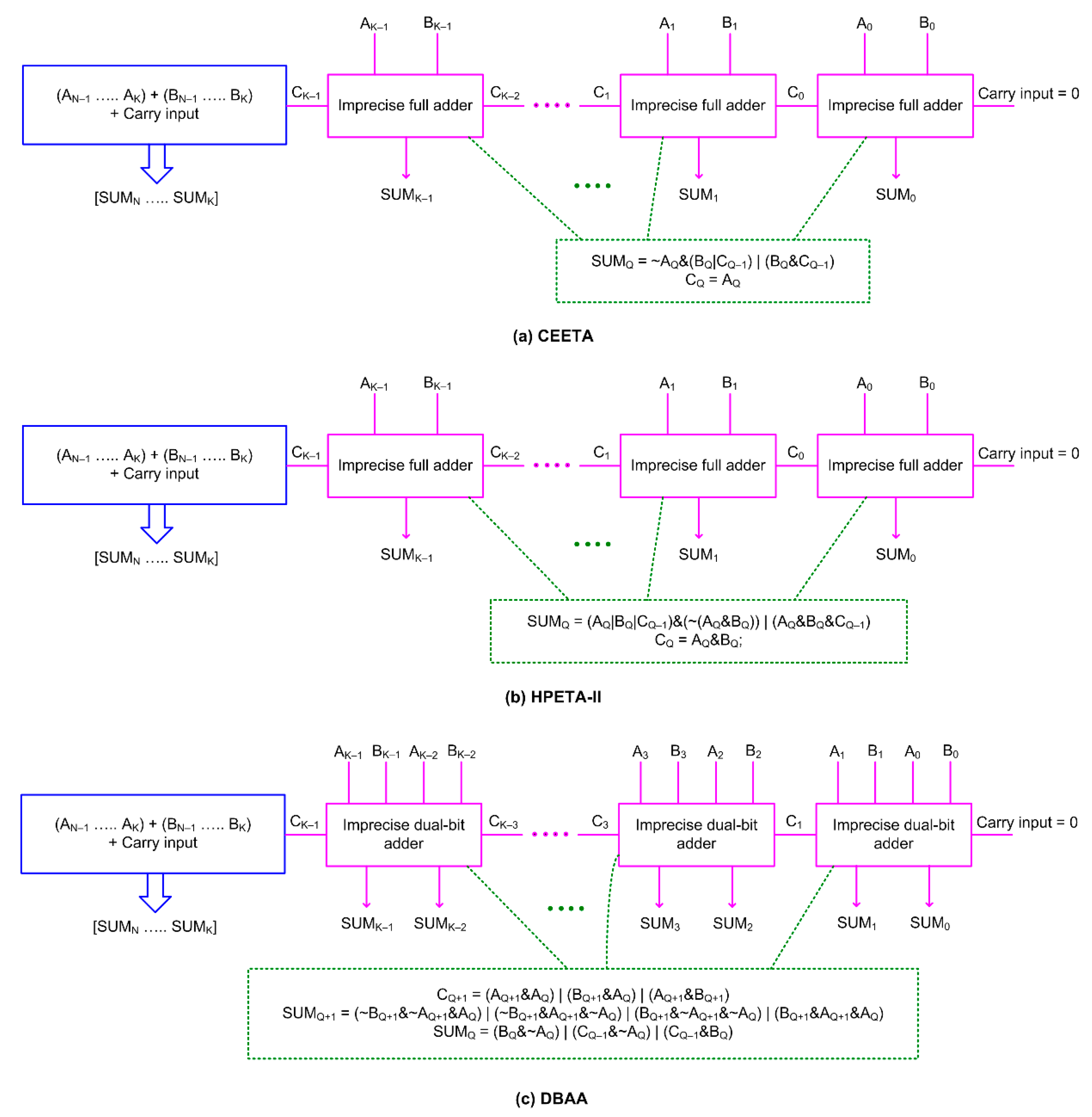
2. Acronyms and Expansions

The acronyms of inaccurate adders and their expansions are given below for a ready reference.
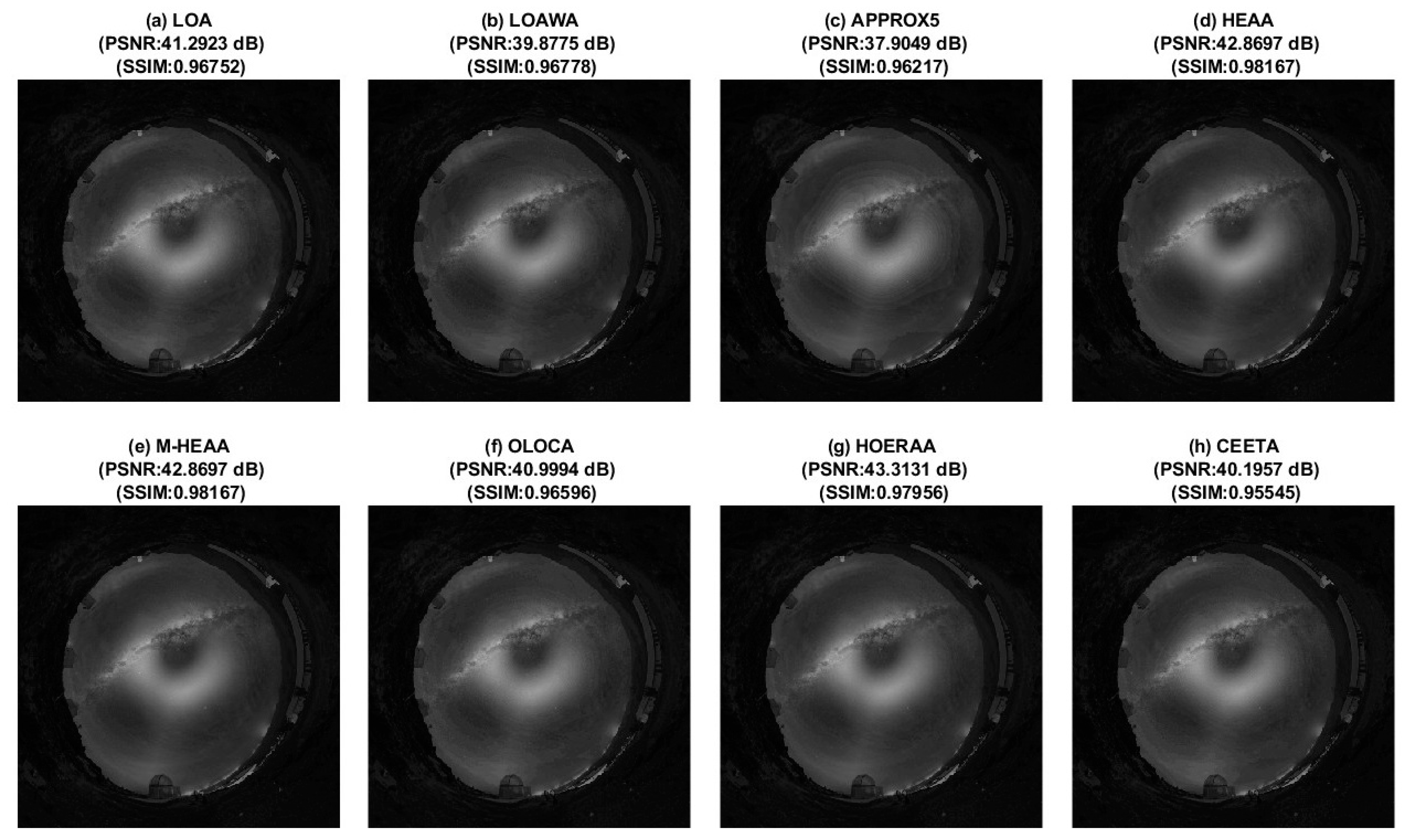
  • LOA [21]: Lower-part OR adder
  • LOAWA [22]: LOA without any carry input provided from the imprecise part to the precise part, as labeled in [27]
  • APPROX5 [23]: An approximate adder utilizing the approximate mirror adder 5 (AMA5) for the imprecise part, as labeled in [27]
  • HEAA [24]: Hardware efficient approximate adder, as labeled in [27]
  • M-HEAA: Modified HEAA [25]
  • OLOCA [26]: Optimized LOA with a constant 1 assigned for (K–2) sum bits of the imprecise part, where K is the size of the imprecise part of an N-bit OLOCA
  • HOERAA [27]: Hardware optimized and error reduced approximate adder
  • HOAANED: Hardware optimized approximate adder with a near-normal error distribution [28]
  • HERLOA: Hybrid error reduction LOA [29]
  • M-HERLOA: Modified HERLOA [30]
  • ERCPAA: Error reduced carry prediction approximate adder [31]
  • COREA: Carry OR error reduced adder [32]
  • CEETA: Compact energy efficient error tolerant adder [33]
  • HPETA-II: High performance error tolerant adder II, as shown in Figure 12 of [34]
  • DBAA: Double bit (adder based) approximate adder [35], labeled as DBAA here
  • SAAR: Segmented approximate adder [36]

3. Architectures of Inaccurate Adders
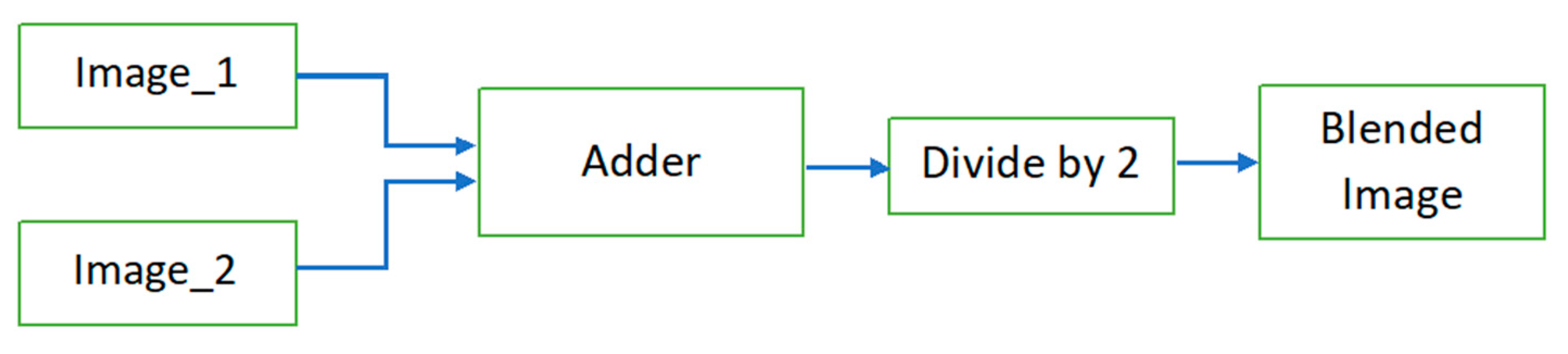
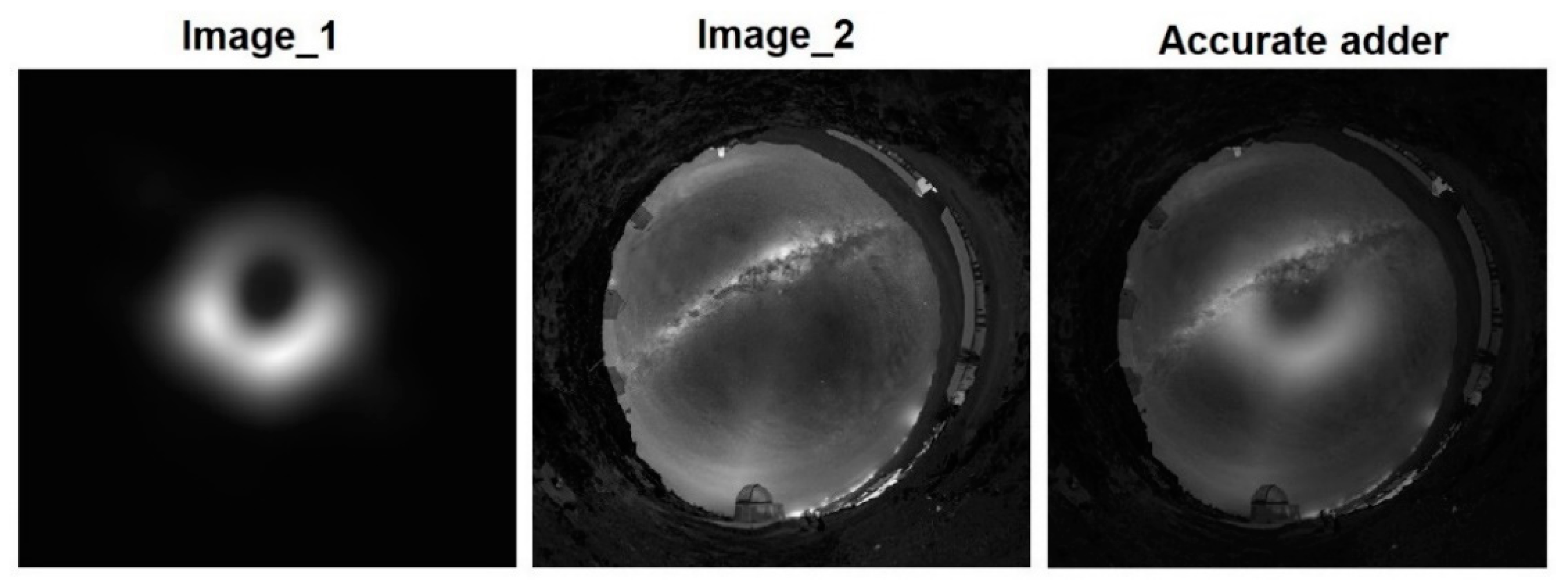
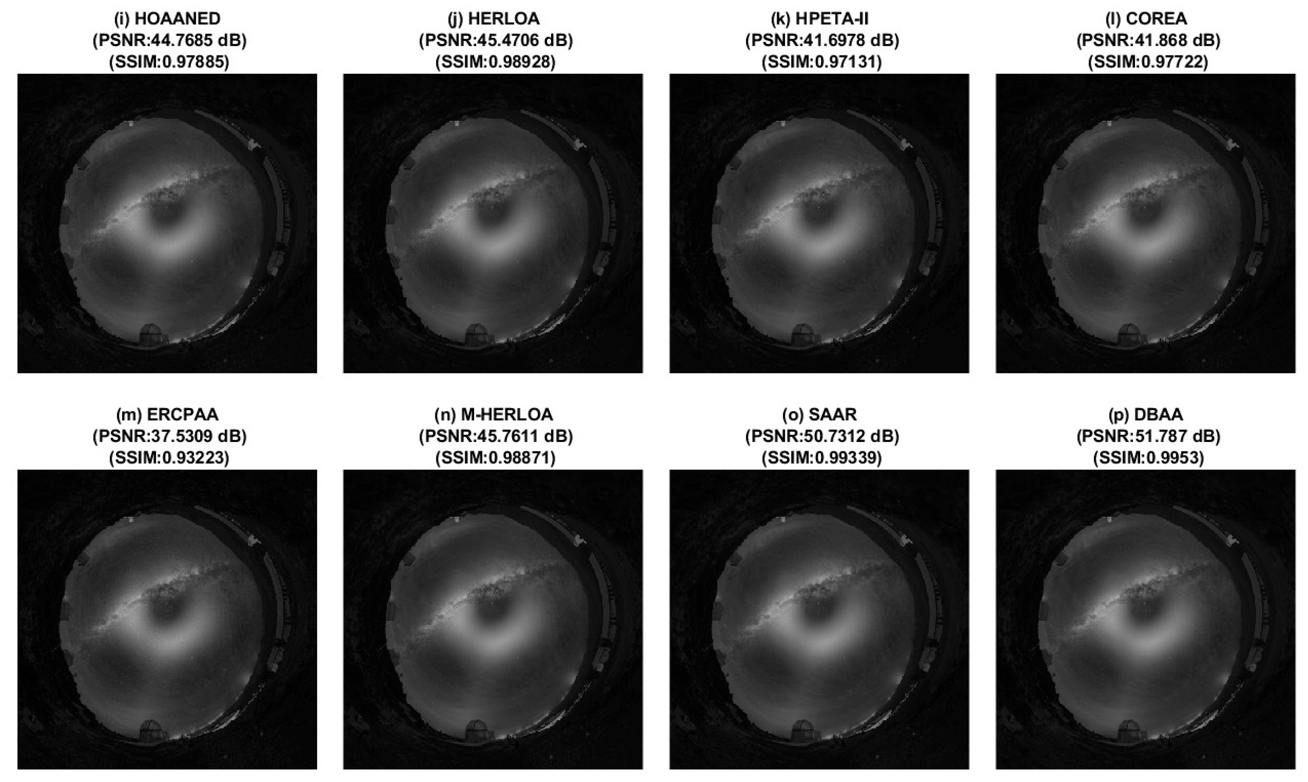
The architectures of many static inaccurate adders presented in [21,22,23,24,25,26,27,28,29,30,31,32,33,34,35,36], which are suitable for implementation in FPGA and ASIC design environments, will be described in this section.
Let us assume that A and B are the two inputs given to an adder and SUM is its output. With N denoting the adder size, AN–1 and BN–1 represent the most significant input bits and A0 and B0 represent the least significant input bits. The adder sum is represented by SUMN to SUM0, with SUMN being the most significant and SUM0 being the least significant. SUMN represents any carry overflow resulting from the addition. The architectures of many inaccurate adders are shown in Figure 1, Figure 2 and Figure 3. Typically, a static inaccurate adder would have a precise part and an imprecise part [3]. The precise part is highlighted in blue and the imprecise part is highlighted in pink in Figure 1, Figure 2 and Figure 3. The addition is performed exactly in the precise part and inexactly in the imprecise part of an inaccurate adder. The precise part is more significant than the imprecise part. Hence, a group of less significant adder inputs is allocated to the imprecise part and the remaining more significant adder inputs are allocated to the precise part of an inaccurate adder. Nevertheless, the number of adder inputs to be allocated to the precise and imprecise parts of an inaccurate adder would depend upon the maximum inaccuracy tolerable for a practical application.
In Figure 1 and Figure 2, K denotes the number of input bits allocated to the imprecise part of the inaccurate adders. Hence, (N–K) input bits would be allocated to the precise part of the inaccurate adders. In Figure 1 and Figure 2, AK–1 up to A0 and BK–1 up to B0 are given to the imprecise part and AN–1 up to AK and BN–1 up to BK are given to the precise part of the inaccurate adders. SUMN to SUMK is produced by the precise part and SUMK–1 to SUM0 is produced by the imprecise part and these two are concatenated to represent the sum output of an inaccurate adder.
The logic corresponding to the precise parts of inaccurate adders (shown in Figure 1 and Figure 2) is identical with or without the exception of any carry input and the fundamental differences between the inaccurate adders are manifest in their imprecise parts. Therefore, we shall only discuss the imprecise parts of inaccurate adders shown in Figure 1 and Figure 2. It may be noted that, for an FPGA implementation, the precise part of an inaccurate adder can be realized using the native FPGA adder which is accurate and high-speed and, for an ASIC type standard cell-based implementation, the precise part may be realized using an area-efficient adder such as the carry ripple adder or a high-speed adder such as a carry-lookahead adder, depending upon the size of the precise part.
In the case of LOA [21], shown in Figure 1a, the sum bits of the imprecise part i.e., SUMK–1 to SUM0, are produced by a logical OR of the respective adder input bits. AK–1 and BK–1 are logically AND-ed and given as the carry input to the precise part.
The imprecise part of LOAWA [22], shown in Figure 1b, is the same as LOA but there is no carry input provided from the imprecise part to the precise part.
In the case of APPROX5 [23], shown in Figure 1c, BK–1 up to B0 are forwarded as the sum bits of the imprecise part viz. SUMK–1 up to SUM0. AK–1 is given as the carry input to the precise part and AK–2 up to A0 are discarded.
In the case of HEAA [24], shown in Figure 1d, SUMK–2 up to SUM0 are produced by a logical OR of the respective adder input bits like that of LOA. AK–1 and BK–1 are logically AND-ed and given as the carry input to the precise part and as the select input (S) of a multiplexer—if S is 0, the logical OR of AK–1 and BK–1 produces SUMK–1 and in case of S is 1, SUMK–1 would assume 0.
M-HEAA [25], shown in Figure 1e, is a modification of HEAA in that SUMK–3 up to SUM0 are fixed as 1 while the logic of SUMK–1 and SUMK–2 is the same as that of HEAA.
OLOCA [26], shown in Figure 1f, is a modification of LOA in that SUMK–3 up to SUM0 are fixed as 1 but the logic of SUMK–1 and SUMK–2 is the same as that of LOA.
In the case of HOERAA [27], shown in Figure 1g, SUMK–3 up to SUM0 are fixed as 1 while SUMK–2 is produced by a logical OR of AK–2 and BK–2. AK–1 and BK–1 are logically AND-ed and given as the carry input to the precise part and as the select input (S) of a multiplexer—if S is 0, the logical OR of AK–1 and BK–1 produces SUMK–1; if S is 1, the logical AND of AK–2 and BK–2 produces SUMK–1.
Just as in HOERAA, in HOAANED [28], shown in Figure 1h, SUMK–3 up to SUM0 are fixed as 1 while SUMK–2 is produced by a logical OR of AK–2 and BK–2. AK–1 and BK–1 are logically AND-ed and given as the carry input to the precise part and as the select input (S) of a multiplexer—if S is 0, the logical OR of AK–1 and BK–1 and the logical AND of AK–2 and BK–2 is OR-ed to produce SUMK–1; otherwise if S is 1, the logical AND of AK–2 and BK–2 produces SUMK–1.
HERLOA [29], shown in Figure 1i, employs a unique logic for its imprecise part and M-HERLOA [30], shown in Figure 1j, is derived from HERLOA where some of the least significant sum bits in the imprecise part are fixed as 1 while the rest of the more significant sum bits in the imprecise part have the same logic as HERLOA. The optimum number of less significant sum bits which may be assigned a 1 in the imprecise part of HERLOA to derive M-HERLOA is, however, best decided based on a target application. In Figure 1j, SUMK–5 up to SUM0 are fixed as 1 while the logic of SUMK–1 to SUMK–4 is maintained the same as in Figure 1i.
In the case of ERCPAA [31], shown in Figure 1k, the imprecise part is further split into two sub-parts of sizes L bits and (K–L) bits. The EXOR of AK–1 and BK–1 and the AND of AK–2 and BK–2 are logically NAND-ed and forwarded as sum bits SUML–1 up to SUM0, while a unique logic is used to produce the remaining (K–L) sum bits of the imprecise part.
COREA [32], shown in Figure 1i, is similar to LOAWA in the sense that its precise part does not accept a carry input from the imprecise part. However, it is somewhat different from the inaccurate adders discussed above in that the least significant sum bit of the precise part viz. SUMK* is not issued directly; rather it is coupled with the AND of the most significant input bit pair of the imprecise part to produce the actual SUMK. The carry generated from the (K+1)-th bit of the precise part is considered as an internal carry input to produce the sum bits of the precise part. Similar to ERCPAA, in COREA, the imprecise part is sub-divided into two sub-parts having sizes L bits and (K–L) bits, but the L sum bits in COREA i.e., SUML–1 up to SUM0 are fixed as 1 and a unique logic is used to generate the remainder of the sum bits corresponding to the imprecise part.
Figure 2 shows the architectures of some inaccurate adders which feature a carry-ripple adder structure in the imprecise part with the structure comprising a cascade of imprecise full adders or dual-bit adders. Though many works in the literature utilized this approach, there could be a possible drawback associated. If a substantially bigger imprecise part than the precise part may be affordable in an inaccurate adder (depending upon the application), the carry may propagate serially in the imprecise part which could result in a greater propagation delay, even exceeding the maximum propagation delay of the precise part. The image blending application considered in this work permits the use of a small precise part and a big imprecise part in an inaccurate adder and in such a scenario the adder’s speed would be affected. This issue is discussed in the subsequent sections. Therefore, to avoid the possibility of a serial carry propagation in the imprecise part of an inaccurate adder that has a cascade of full adders/dual-bit adders, it would be best to ensure that the carry output of a full adder/dual-bit adder is not dependent on the carry input but only on the primary inputs. Figure 2a,b shows two such inaccurate adders namely CEETA [33] and HPETA-II [34], which feature a cascade of imprecise full adders in the imprecise part, and the carry output of the imprecise full adders only depends on the adder’s primary inputs. The sum and carry output equations of the imprecise full adders used in CEETA and HPETA-II are given in Figure 2a,b within the dotted green boxes.
Figure 2c [35] shows an inaccurate adder that uses a cascade of imprecise dual-bit adders to realize the imprecise part. A dual-bit adder, which is logically equivalent to two one-bit full adders, adds two input bit pairs at the same time along with any carry input and produces two sum bits and a carry output. Reference [35] has considered the use of imprecise dual-bit adders by modifying the logic of a precise dual-bit adder and we refer to the inaccurate adder presented in [35] as a dual-bit approximate adder (DBAA) here for reference.
Figure 3 shows another inaccurate adder called SAAR [36], which is a segmented inaccurate adder. According to SAAR architecture, an N-bit adder is split into accurate adder segments which may or may not be equal in size. Excepting the least significant accurate adder segment, the remaining more significant accurate adder segments receive carry inputs from custom carry generators, as shown in Figure 3. The generalized logic expression of the carry output produced by a carry generator is also given in Figure 3.

4. Image Blending

We considered an image blending application to analyze and compare the performance of inaccurate adders versus the accurate adder. We performed blending of two 16-bit grayscale images in MATLAB (version R2022a) and we utilized the accurate adder and inaccurate adders discussed in the previous section individually to perform image blending as illustrated in Figure 4.
Equation (1) was used to perform image blending. In (1), α is a constant parameter that is used to decide the extent of each image that should be manifest in the blended image. To give equal weightage to both the images (i.e., Image_1 and Image_2) in the blending, we considered α = 0.5. On substituting α = 0.5 in (1), Equation (2) results.
Blended Image = α (Image_1) + (1 − α) Image_2
Blended Image = 0.5 (Image_1 + Image_2)
The quality of blended images obtained using accurate and inaccurate addition was evaluated using standard metrics such as the peak signal-to-noise ratio (PSNR) [37] and the structural similarity index measure (SSIM) [38]. A high PSNR implies less noise/distortion which is preferable and PSNR is measured in dB. SSIM quantifies the similarity between a reference image and a target image and a high SSIM is also preferred. SSIM is more relevant for digital image processing and it varies from decimal 0 to 1 with 0 indicating no match and 1 indicating a perfect match between the reference and target images.
We used two 16-bit images namely ‘La Silla’ [39] and ‘Black Hole’ [40] from the European Southern Observatory database to perform image blending. The original size of the La Silla image is 10,000 × 10,000 pixels and the original size of the Black Hole image is 7416 × 4320 pixels. The dimensions of these images are huge and so the background of the images was cropped without affecting the main form or texture of the images and the two images were reduced in size. When the size of an image is reduced, its spatial resolution is also reduced and thus the two images were reduced to the same size of 512 × 512 pixels for faster processing and to perform blending. A further reduction of the image size (which would also reduce the spatial resolution) was found to affect the information contained in the images and hence this was avoided. Moreover, the colored images were converted into grayscale images—this is because, while performing blending, the focus is on image intensity rather than color. To perform image blending accurately, we used a 16-bit accurate adder, and to perform image blending inaccurately we used different 16-bit inaccurate adders individually. Since the inaccurate adders shown in Figure 1 and Figure 2 comprise a precise part and an imprecise part, we determined the optimum inaccuracy that could be incorporated in an inaccurate adder which would be suitable for image blending through repeated experimentation, i.e., trial-and-error.
In general, an optimum (maximum acceptable) inaccuracy helps to achieve a good trade-off between sacrifice in output quality and savings in design metrics. A less-than-optimum inaccuracy can improve the output quality due to relatively fewer errors but would reduce the maximum savings in design metrics achievable. A more-than optimum inaccuracy would degrade the output quality due to more errors introduced but would increase the savings in design metrics achievable over accurate computation. These observations have been validated for an image reconstruction application in [28]. Given these, the objective is to ascertain an optimum inaccuracy that would be deemed acceptable for a practical application. For the image blending application, we found out through trial-and-error that having a 4-bit precise part and a 12-bit imprecise part in a 16-bit inaccurate adder represents an optimum inaccuracy for many inaccurate adders and this applies to the inaccurate adders shown in Figure 1 and Figure 2. The architecture of SAAR is however different and a 16-bit SAAR portrayed in [36] was considered as it is, which has been shown in Figure 3.
Figure 5 shows the ‘Black Hole’ image (referred to as Image_1), the ‘La Silla’ image (referred to as Image_2) and the blended image obtained using accurate addition. The results of image blending obtained using inaccurate addition corresponding to an optimum inaccuracy are shown in Figure 6. In Figure 6, the names of the inaccurate adders and the respective PSNR and SSIM of the blended images are specified on the top of the images for quick reference.
It can be seen from Figure 6 that the blended images obtained using many inaccurate adders are of acceptable quality. As mentioned earlier, it is preferable to have high PSNR and particularly high SSIM for an image that reflects the good quality. Given this, from Figure 6, it is observed that DBAA achieves the highest PSNR and SSIM compared to its counterparts. Based on SSIM, inaccurate adders HERLOA, M-HERLOA and SAAR are close to DBAA based on PSNR and SAAR is close to DBAA. Nevertheless, besides output quality, the savings in design metrics achieved by an inaccurate adder over an accurate adder is also important to consider to determine which inaccurate adder(s) is/are preferable from the combined perspectives of output quality and savings in the design metrics. In this context, the next section presents the calculated error metrics and the estimated design metrics of various inaccurate adders.

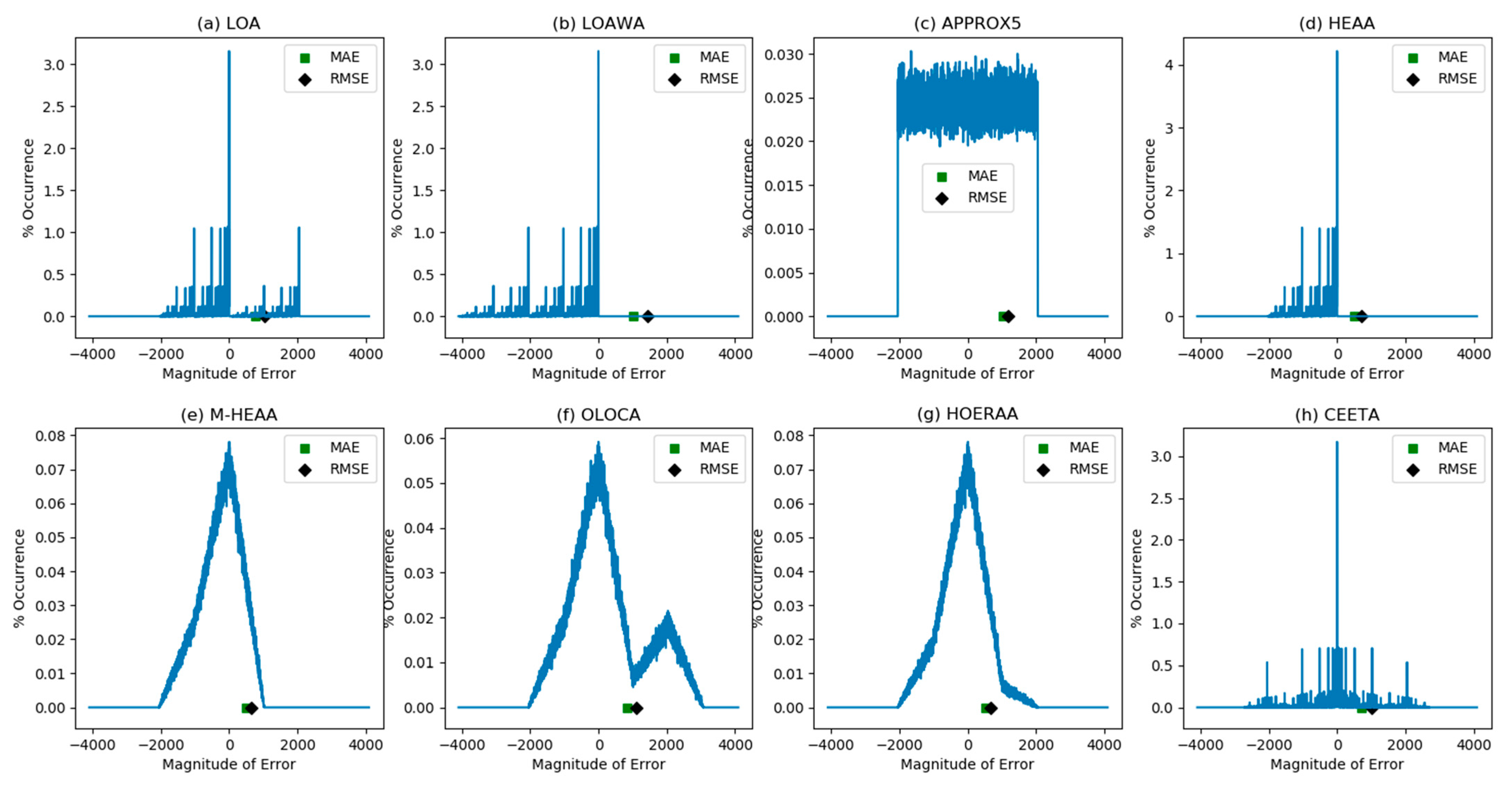
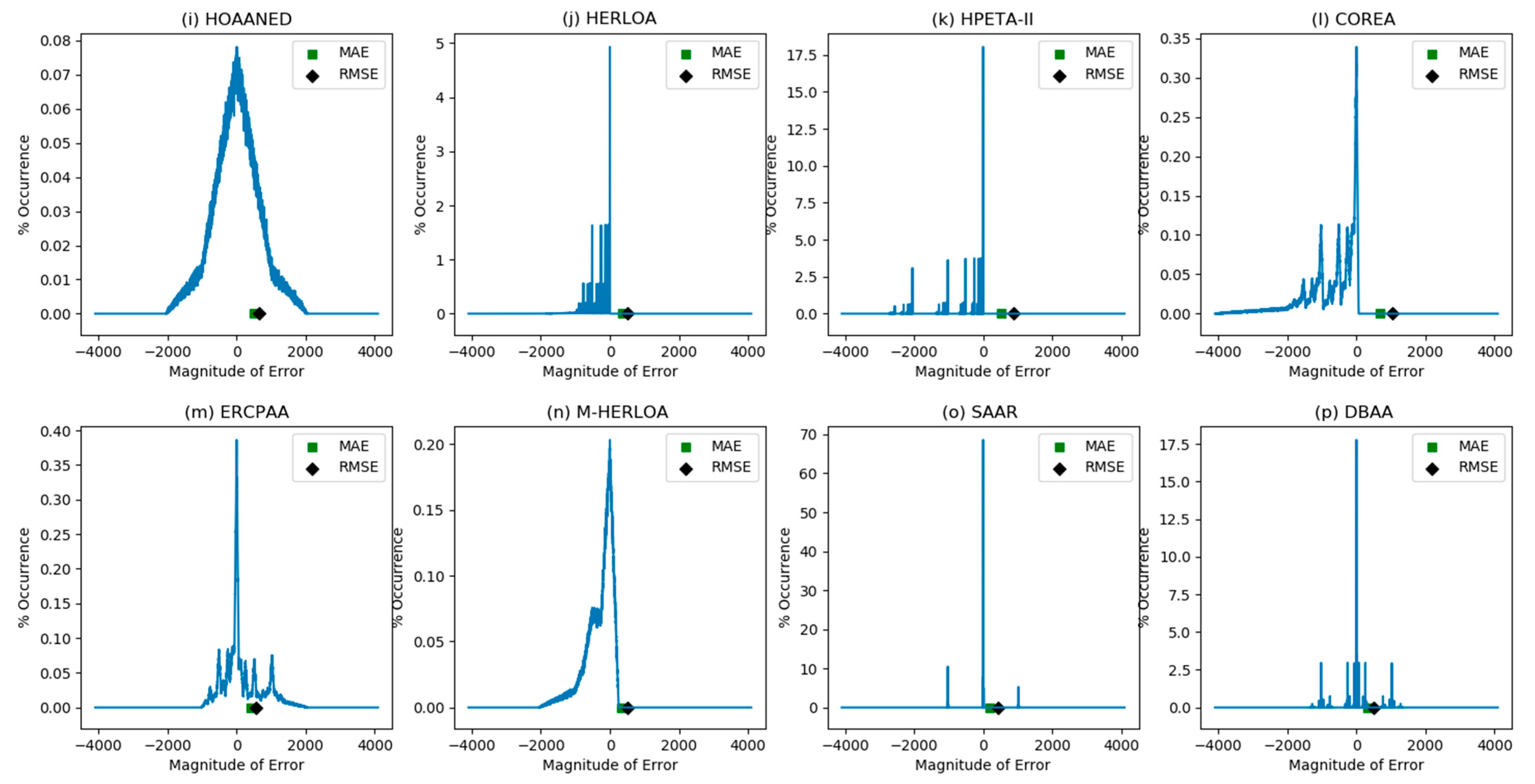
5. Error Characteristics and Error Metrics of Inaccurate Adders

Typically, the quality of a blended image obtained using an inaccurate adder is given higher priority than the savings in design metrics gained by it over the accurate adder. In this context, this section presents the error characteristics and the calculated error metrics of various inaccurate adders.
We calculated the error metrics of 16-bit inaccurate adders shown in Figure 1 and Figure 2 corresponding to an optimum inaccuracy, with the inaccurate adders having a 4-bit precise part and a 12-bit imprecise part, as mentioned earlier. Since SAAR is architecturally different from the other inaccurate adders, its error metrics were calculated according to the circuit shown in Figure 3. We calculated two popular error metrics, namely the mean absolute error (MAE, which is also called the mean error distance) and the root means square error (RMSE). However, RMSE is a better metric to characterize the extent of signal degradation in a digital signal processing application [41]. We modeled the high-level functionality of the accurate adder and various inaccurate adders in Python. A 16-bit adder has a total of 232 inputs which would be cumbersome to consider. Hence, we supplied a million randomly generated inputs to the adders and calculated the MAE and RMSE of inaccurate adders relative to the correct sum produced by the accurate adder. MAE and RMSE were calculated using Equations (3) and (4), respectively, which are given below.
MAE = 1 M P = 1 M | InaccuSum ( A P , B P ) AccuSum ( A P , B P )   |
RMSE = 1 M P = 1 M ( InaccuSum ( A P , B P ) AccuSum ( A P , B P ) ) 2
In Equations (3) and (4), AccuSum ( A P , B P ) represents the sum produced by the accurate adder, InaccuSum ( A P , B P )   represents the sum produced by an inaccurate adder and the notation ( A P , B P ) denotes one set of adder inputs. M represents the number of inputs supplied to the adders for calculation of the error metrics and here, M = 1,000,000.
MAE and RMSE calculated for the inaccurate adders are given in Table 1. The absolute difference between the sum outputs of inaccurate adders and the sum output of the accurate adder, corresponding to the inputs applied, is captured in the form of an error distribution plot which is shown in Figure 7. The error distribution plot shows the magnitude of errors of the inaccurate adders as a function of their percentage occurrence, corresponding to the inputs applied. The error distribution plot portrays the error characteristics of inaccurate adders. MAE and RMSE calculated for the inaccurate adders are also highlighted in Figure 7. From Table 1, it is seen that SAAR reports the least MAE and RMSE among its counterparts. This is possible because SAAR, as seen in Figure 3, has a 6-bit significant accurate adder segment while the other inaccurate adders have a 4-bit significant precise part corresponding to an optimum inaccuracy. This explains why SAAR features relatively lesser error occurrences compared to the other inaccurate adders in the error distribution plot shown in Figure 7.
From Figure 7, it is seen that SAAR features a significantly greater percentage of zero error occurrences compared to the other inaccurate adders. This is the reason behind SAAR reporting lesser MAE and RMSE compared to its counterparts in Table 1. In the case of DBAA, although the percentage of zero error occurrences is lesser compared to SAAR, nevertheless, the distribution of errors with positive and negative magnitudes is rather balanced concerning the zero mid-point which is the reason behind the less MAE and RMSE of DBAA. These explain why SAAR and DBAA were found to yield almost the same high-quality blended image, as noted in the previous section, which is closely followed by HERLOA and M-HERLOA. In Table 1, it is seen that M-HERLOA features lesser MAE and RMSE than HERLOA.

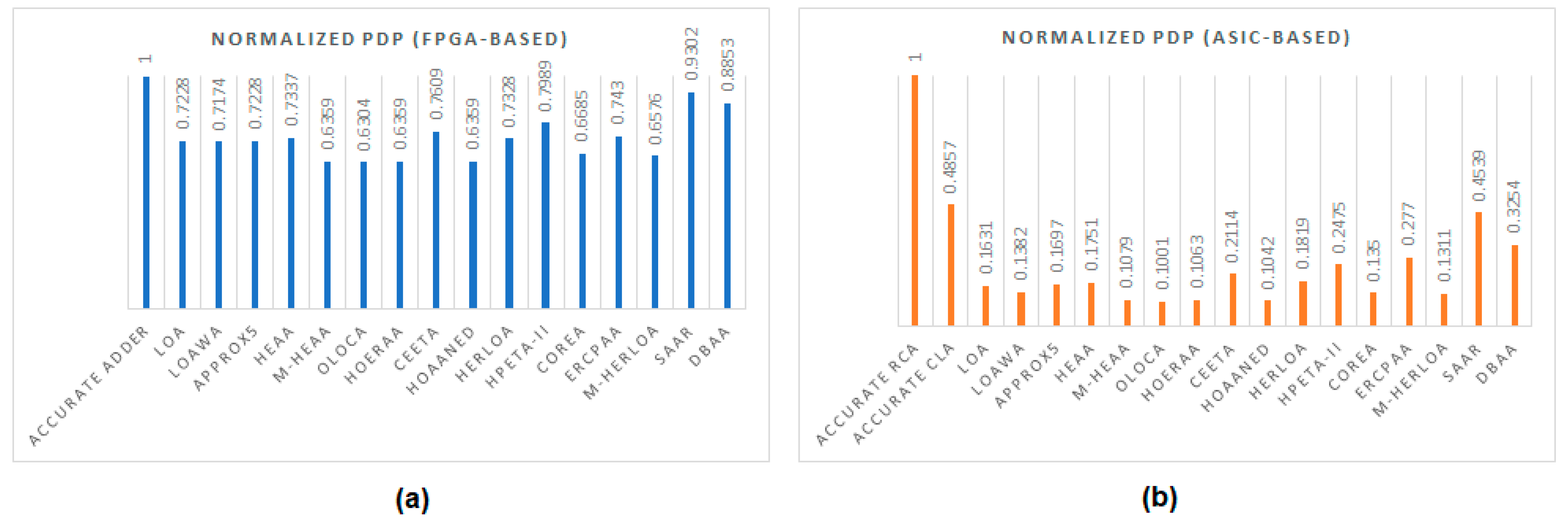
6. Design Metrics of Accurate and Inaccurate Adders

In this section, we present the physical design metrics of accurate and inaccurate adders, implemented in FPGA and ASIC design environments. Since the inaccurate adders discussed in Section 2 are suitable for both FPGA and ASIC type implementations, both these design platforms were considered for physical realization.

6.1. FPGA-Based Implementation

For an FPGA implementation, we described the accurate 16-bit adder and inaccurate 16-bit adders in Verilog HDL at the behavioral level. The inaccurate 16-bit adders, shown in Figure 1 and Figure 2, correspond to an optimum inaccuracy, i.e., having a 4-bit precise part and a 12-bit imprecise part, and the 16-bit SAAR was described as shown in Figure 3. The high-speed carry logic inherent in an FPGA slice was utilized to realize the high-speed accurate adder. The precise parts of the inaccurate adders were also realized for high-speed likewise. All the adders were synthesized and implemented on a Xilinx Artix-7 FPGA (part: xc7a100tcsg324-3) using the Xilinx Vivado design tool (version 2018.3). A pair of input registers was provisioned before the adder inputs to eliminate the input-output routing delay from dominating the adder’s delay. An output register followed the adder outputs. The Flow_AreaOptimized_high strategy was used for synthesis and the default implementation strategy was used. The design metrics of the 16-bit accurate adder and 16-bit inaccurate adders are given in Table 2, which include the number of look-up tables (LUTs) utilized, the number of registers (flip-flops) utilized, delay i.e., minimum clock period, and the total on-chip power consumption which is the sum of the power consumed by the clock, signals, logic, and input-output. FPGA-based design metrics were estimated after placement and routing.
In general, it is observed from Table 2 that all the inaccurate adders have a reduced delay compared to the delay of the accurate adder. This is because, considering an optimum inaccuracy, the precise part of the inaccurate adders shown in Figure 1 and Figure 2 is only of 4-bits size compared to the accurate adder which has a 16-bit precise part. SAAR, shown in Figure 3, has a critical path comprising a carry generator and a 6-bit accurate adder segment. Therefore, compared to the accurate 16-bit adder, SAAR is also expected to have reduced critical path delay, which is found to be true in Table 2. Nevertheless, the speed of the inaccurate adders is constrained by the maximum speed of the interconnect in the FPGA fabric. Since the inaccurate adders have an imprecise part, whose logic is reduced compared to the accurate adder, this should lead to potential reductions in resource utilization and power consumption for the inaccurate adders compared to the accurate (FPGA) adder.
From Table 2, we see the accurate (FPGA) adder and some inaccurate adders viz. LOA, LOAWA, HEAA, HPETA-II and SAAR utilize the same number of LUTs and registers. However, since the imprecise parts of LOA, LOAWA, HEAA and HPETA-II have reduced logic compared to the accurate adder, they consume relatively less on-chip power.
Among the inaccurate adders, APPROX5 utilizes the least number of LUTs. This is because in APPROX5, input bits A10 up to A0 are not used, thus saving 11 registers compared to the accurate adder and hence APPROX5 consumes less power compared to the accurate adder. Concerning M-HEAA, OLOCA, HOERAA and HOAANED, sum bits Sum9 up to Sum0 are fixed as 1 and so input bits A9 up to A0 and B9 up to B0 are not used. These lead to a combined savings of 30 registers for M-HEAA, OLOCA, HOERAA and HOAANED compared to the accurate adder, which translates into reductions in their on-chip power consumption. In the case of M-HERLOA, sum bits Sum7 up to Sum0 are fixed as 1 and thus input bits A7 up to A0 and B7 up to B0 are not used—these lead to a combined savings of 24 registers for M-HERLOA compared to the accurate adder resulting in a reduced on-chip power compared to the accurate adder. CEETA, HPETA-II, SAAR and DBAA have logic corresponding to all the sum bits in their precise and imprecise parts. Hence, they utilize the same number of registers as the accurate adder. HPETA-II and SAAR utilize the same number of LUTs as the accurate adder. Therefore, CEETA, HPETA-II and DBAA consume greater power than the other inaccurate adders and SAAR is found to consume slightly more power than even the accurate FPGA adder. This is because SAAR embeds more logic than the other inaccurate adders since its adder segments are accurate and besides that, SAAR incorporates two carry generators. SAAR achieves a reduction in delay by just 8.7% compared to the accurate adder but consumes 2% more power and utilizes the same number of LUTs and registers as the accurate adder. On the other hand, DBAA utilizes 19% fewer LUTs than the accurate adder but consumes the same number of registers. DBAA reports just a 1.6% reduction in delay compared to the accurate adder which is marginal and it consumes 10% less power than the accurate FPGA adder.
It may be recalled that in Section 4 (referring to Figure 6), it was noted that after SAAR and DBAA, HERLOA and M-HERLOA are preferable for image blending. HERLOA and M-HERLOA yielded almost the same quality of the blended image and, from Table 1, it was noted that M-HERLOA reported reduced MAE and RMSE compared to HERLOA. From Table 2, we see that M-HERLOA utilizes 33.3% fewer LUTs and 49% fewer registers and consumes 9.7% less on-chip power compared to HERLOA while having almost the same delay. This is mainly because the least significant sum bits Sum7 up to Sum0 are fixed as 1 in M-HERLOA, unlike HERLOA which leads to reductions in logic and on-chip power for the former compared to the latter. Hence, M-HERLOA is preferable to HERLOA. Compared to M-HERLOA, SAAR utilizes 100% more LUTs and 96% more registers, has 5% greater delay, and consumes 34.7% more power. On the other hand, DBAA utilizes 62.5% more LUTs and 96% more registers, has 13.1% greater delay, and consumes 19% more power compared to M-HERLOA. Nevertheless, to make an informed judgment about whether M-HERLOA is more efficient, the design metrics of different inaccurate adders corresponding to an ASIC type standard cell-based implementation should also be considered and this is presented next.

6.2. ASIC-Type (Standard Cell-Based) Implementation

Accurate and inaccurate adders were also realized using a 32/28 nm CMOS standard digital cell library [42]. Since the inaccurate adders shown in Figure 1 and Figure 2 have a small 4-bit precise part (corresponding to an optimum inaccuracy), their precise part was synthesized using a ripple carry adder (RCA) structure by describing the precise parts behaviourally in Verilog HDL. The accurate adder segments of SAAR, shown in Figure 3, are small. Hence, they were also synthesized as an RCA. Using an RCA structure helps to minimize the area and power dissipation of the inaccurate adders. Two accurate adders were synthesized, namely an accurate 16-bit RCA and an accurate 16-bit carry look-ahead adder (CLA). RCA typically consumes less area and dissipates less power while being slow, whereas the CLA is relatively faster but consumes more area and dissipates more power in comparison. To realize an accurate CLA, a high-speed CLA design presented in [43] was used where a 16-bit CLA was constructed using four 4-bit CLAs. The accurate CLA was described in Verilog HDL at the gate level, according to the architecture shown in [43], and then synthesized. Synopsys Design Compiler was used for synthesis with the synthesis option specified as ‘compile_ultra’ to synthesize the accurate RCA and the inaccurate adders; the synthesis option was specified as ‘compile’ with optimization for high-speed to synthesize the accurate CLA. A test bench comprising several randomly generated inputs was supplied to the gate-level netlists of accurate and inaccurate adders at a time period of 2ns (500 MHz) to perform functional simulations and to record their switching activity, which was subsequently used for power estimation using Synopsys PrimePower. Synopsys PrimeTime was used to estimate the critical path delay of accurate and inaccurate adders. A default wire load model was adopted during synthesis and the total area of the adders including cells area and interconnect area was estimated using Synopsys Design Compiler. The ASIC-based design metrics i.e., total area, critical path delay, and average (total) power dissipation of accurate and inaccurate adders estimated are given in Table 3.
As expected, it is seen from Table 3 that the accurate RCA occupies a lesser area and dissipates less power than the accurate CLA but the accurate CLA is relatively faster. From Table 3, it is seen that excepting ERCPAA and SAAR, all the other inaccurate adders report reductions in all the design metrics compared to the accurate RCA and CLA. This is mainly because of the small precise part and a relatively big imprecise part affordable in the inaccurate adders corresponding to an optimum inaccuracy. As a result, many of the inaccurate adders have reduced logic and a shortened critical path which translates into reductions in area, power, and delay compared to the accurate adders. The area occupancy of DBAA is however close to the RCA and this is because its imprecise part is composed of dual-bit adders which require more logic. Nevertheless, the critical path of DBAA traverses through a carry logic present in an imprecise dual-bit adder and a 4-bit RCA, which is shorter than the critical paths of accurate RCA and CLA. Though the delay of ERCPAA and SAAR is less than the delay of the accurate RCA, it is not so in comparison with the delay of the accurate CLA.
Let DXOR2, DAO21, DOR4, DAND4, DFA, DAND2, DOR2 and DAO22 represent the typical propagation delays of a 2-input XOR gate, an AO21 complex gate, a 4-input OR gate, a 4-input AND gate, a full adder, a 2-input AND gate, a 2-input OR gate and an AO22 complex gate, respectively. Given these, the delay of the accurate 16-bit CLA is expressed by DCLA = (DXOR2 + DAO21) + 2 × DAO21 + (DOR4 + DAND4 + DXOR2) based on [43]; the delay of 16-bit ERCPAA is expressed by DERCPAA = 4 × DFA + (DXOR2 + DAND2 + DOR2); and the delay of 16-bit SAAR is expressed by DSAAR = 6 × DFA + DAO22. Using the typical propagation delays of gates present in the standard cell library [42], the theoretical delay (excluding the interconnect delay) of the accurate CLA, ERCPAA, and SAAR was calculated to be 0.529 ns, 0.579 ns, and 0.572 ns respectively. This shows that the accurate CLA has less delay than the delays of the inaccurate adders ERCPAA and SAAR and the theoretical delay calculation tallies with the practical delay estimates of CLA, ERCPAA, and SAAR given in Table 3.
From Table 3, we see that OLOCA occupies the least area and dissipates the least power and LOAWA reports the least delay compared to the other inaccurate adders. However, as seen in Table 1 and Figure 7, OLOCA and LOAWA report high MAE and RMSE and feature a high number of non-zero error occurrences. Moreover, from Table 2, LOAWA is found to utilize the same number of LUTs and registers as the accurate FPGA adder. From Figure 6, we observe that OLOCA and LOAWA yield blended images of somewhat inferior quality compared to many other inaccurate adders, i.e., the PSNR and SSIM of the blended image obtained using OLOCA and LOAWA are lesser compared to the PSNR and SSIM of blended images obtained using other inaccurate adders, namely LOA, HEAA, M-HEAA, HOERAA, HOAANED, HERLOA, HPETA-II, COREA, SAAR, M-HERLOA, and DBAA.
In Section 4 (Figure 6), SAAR and DBAA were found to yield almost the same high-quality blended image compared to the other inaccurate adders and this is attributed to their relatively reduced error metrics and better error characteristics. However, both HERLOA and M-HERLOA were found to be close to SAAR and DBAA in achieving similar high-quality blended images (especially in terms of SSIM), as seen in Figure 6. In Table 2, M-HERLOA was found to be better than HERLOA in terms of utilizing fewer resources and consuming less power while having the same delay for an FPGA-based implementation. From Table 3, we see that M-HERLOA occupies 24% less area and dissipates 28% less power than HERLOA while reporting the same delay for an ASIC-type implementation. Therefore, it can be concluded that M-HERLOA outperforms HERLOA. Hence, it would be useful to make a comparison between M-HERLOA and SAAR, DBAA. From Table 3, we note that compared to SAAR, M-HERLOA occupies 51% less area, reports 23.5% less delay, and dissipates 62.3% less power. Compared to DBAA, M-HERLOA occupies 42% less area, reports 4.6% less delay, and dissipates 57.8% less power. Thus, the reductions in design metrics achieved by M-HERLOA over SAAR and DBAA for an ASIC-type standard cell-based implementation (as seen in Table 3) and an FPGA-based implementation (as seen in Table 2) are significant. Since SSIM is an important and more relevant metric for digital image processing and given that M-HERLOA achieves almost the same SSIM for the blended image as SAAR and DBAA, and also because the RMSE of M-HERLOA lies between the RMSE of SAAR and DBAA, thus overall M-HERLOA is found to be preferable compared to its counterparts for performing image blending.
We also calculated the power-delay product (PDP) of accurate and inaccurate adders corresponding to FPGA and ASIC type implementations since PDP is a commonly used figure-of-merit for low power/energy in a digital circuit or system design. Since power and delay are preferred to be less, PDP is also preferred to be less for a digital logic design. We performed a normalization by dividing the actual PDP of accurate and inaccurate adders with the highest actual PDP corresponding to an (accurate) adder for FPGA and ASIC-based implementations separately. The normalized PDP plots are shown in Figure 8a,b for FPGA and ASIC type implementations, respectively, where a normalized PDP value of 1 indicates a design with an inferior low power figure-of-merit. From Figure 8, it is observed that the reduction in PDP attained by inaccurate adders compared to the accurate adder is more significant for ASIC-type implementations compared to FPGA-based implementations. This is mainly because, as mentioned in Section 6.1, the maximum operating speed of an inaccurate adder is constrained by the maximum speed of operation permissible in an FPGA interconnect fabric. However, such a constraint does not manifest for ASIC-type standard cell-based implementations and so the inaccurate adders report significant reductions in critical path delay compared to the accurate RCA (and also accurate CLA).
It was mentioned previously that M-HERLOA is preferable to the other inaccurate adders from the combined perspectives of quality of blended image, error metrics, and design metrics. Given this, M-HERLOA is found to achieve a 34.2% reduction in PDP compared to the accurate adder for an FPGA implementation and an 86.9% (73%) reduction in PDP compared to the accurate RCA (CLA) for an ASIC type implementation. In Figure 8a,b, although OLOCA is found to have the least PDP, the quality of the blended image obtained using OLOCA is not superior to the quality of the blended image obtained using M-HERLOA, as evident from the PSNR and SSIM values shown in Figure 6. Further, the error metrics (MAE and RMSE) of OLOCA are higher compared to M-HERLOA, as seen in Table 1, which is not preferable.

7. Conclusions

This paper analyzed the usefulness of inaccurate addition for digital image blending, which is commonly used in applications such as photo editing and computer graphics. Towards this, we considered many inaccurate adders and evaluated their performance in comparison with the accurate adder. The results showed that certain inaccurate adders can produce almost the same quality of the blended image as accurate addition while enabling significant reductions in the design metrics for implementation in FPGA and ASIC design environments.
Output quality (here, the quality of a blended image), which is dependent upon an inaccurate adder’s error characteristics, and the savings in design metrics gained by an inaccurate adder compared to the accurate adder for FPGA and ASIC type implementations are important to consider in determining a very suitable inaccurate adder. Hence, from the combined perspectives of the quality of the blended image (especially SSIM as given in Figure 6), error metrics (especially RMSE as given in Table 1), and the design metrics corresponding to FPGA and ASIC type implementations (as given in Table 2 and Table 3), it is inferred that M-HERLOA is preferable to its inaccurate adder counterparts. Corresponding to an optimum inaccuracy that is deemed acceptable for image blending, M-HERLOA achieves the following reductions in design metrics compared to the accurate adder: (i) 50% fewer LUTs, 49% fewer registers, 13% reduction in delay, 24.4% reduction in on-chip power and 34.2% reduction in energy compared to the accurate adder for an FPGA based implementation and (ii) 43% (81%) reduction in area, 64.6% (19.5%) reduction in delay, 63% (66.5%) reduction in power and 86.9% (73%) reduction in energy compared to the accurate RCA (CLA) for a standard cell-based ASIC type implementation.

Author Contributions

Conceptualization, P.B. and R.N.; methodology, P.B., R.N. and D.L.M.; software, P.B. and R.N.; validation, P.B. and R.N.; investigation, P.B. and R.N.; resources, D.L.M.; data curation, P.B. and R.N.; writing—original draft preparation, P.B.; visualization, P.B. and R.N.; supervision, P.B. and D.L.M.; project administration, P.B. and D.L.M.; funding acquisition, D.L.M. All authors have read and agreed to the published version of the manuscript.

Funding

This research was funded by the Ministry of Education (MOE), Singapore under grant number MOE2018-T2-2-024.

Data Availability Statement

All data are available within the manuscript.

Conflicts of Interest

The authors declare no conflict of interest. The funders had no role in the design of the study; in the collection, analyses, or interpretation of data; in the writing of the manuscript; or in the decision to publish the results.

References

  1. Han, J.; Orshansky, M. Approximate computing: An emerging paradigm for energy-efficient design. In Proceedings of the 18th IEEE European Test Symposium, Avignon, France, 27–30 May 2013; pp. 1–6. [Google Scholar]
  2. Roy, K.; Raghunathan, A. Approximate computing: An energy-efficient computing technique for error resilient applications. In Proceedings of the IEEE Computer Society Annual Symposium on VLSI, Montpellier, France, 8–10 July 2015; pp. 473–475. [Google Scholar]
  3. Zhu, N.; Goh, W.L.; Zhang, W.; Yeo, K.S.; Kong, Z.H. Design of low-power high-speed truncation-error-tolerant adder and its application in digital signal processing. IEEE Trans. VLSI Syst. 2010, 18, 1225–1229. [Google Scholar]
  4. Zhu, N.; Goh, W.L.; Wang, G.; Yeo, K.S. Enhanced low-power high-speed adder for error-tolerant application. In Proceedings of the International SoC Design Conference, Incheon, Korea, 22–23 November 2010; pp. 323–327. [Google Scholar]
  5. Raha, A.; Jayakumar, H.; Raghunathan, V. Input-based dynamic reconfiguration of approximate arithmetic units for video encoding. IEEE Trans. VLSI Syst. 2016, 24, 846–857. [Google Scholar] [CrossRef]
  6. Breuer, M.A. Multi-media applications and imprecise computation. In Proceedings of the 8th Euromicro Conference on Digital System Design, Porto, Portugal, 30 August–3 September 2005; pp. 1–6. [Google Scholar]
  7. Nair, R. Big data needs approximate computing: Technical perspective. Commun. ACM 2015, 58, 104. [Google Scholar] [CrossRef]
  8. Panda, P.; Sengupta, A.; Sarwar, S.S.; Srinivasan, G.; Venkataramani, S.; Raghunathan, A.; Roy, K. Cross-layer approximations for neuromorphic computing: From devices to circuits and systems. In Proceedings of the 53rd Annual Design Automation Conference, Austin, TX, USA, 5–9 June 2016; pp. 1–6. [Google Scholar]
  9. Sarwar, S.S.; Srinivasan, G.; Han, B.; Wijesinghe, P.; Jaiswal, A.; Panda, P.; Raghunathan, A.; Roy, K. Energy efficient neural computing: A study of cross-layer approximations. IEEE J. Emerg. Sel. Top. Circuits Syst. 2018, 8, 796–809. [Google Scholar] [CrossRef]
  10. Sampson, A.; Deitl, W.; Fortuna, E.; Gnanapragasam, D.; Ceze, L.; Grossman, D. EnerJ: Approximate data types for safe and general low-power computation. In Proceedings of the 32nd ACM SIGPLAN Conference on Programming Language Design and Implementation, San Jose, CA, USA, 4–8 June 2011; pp. 164–174. [Google Scholar]
  11. Sampson, A.; Nelson, J.; Strauss, K.; Ceze, L. Approximate storage in solid-state memories. ACM Trans. Comput. Syst. 2014, 32, 9. [Google Scholar] [CrossRef]
  12. Shoushtari, M.; Rahmani, A.M.; Dutt, N. Quality-configurable memory hierarchy through approximation. In Proceedings of the International Conference on Compilers, Architectures and Synthesis for Embedded Systems, Seoul, Korea, 15–20 October 2017; pp. 1–2. [Google Scholar]
  13. Zhang, H.; Putic, M.; Lach, J. Low power GPGPU computation with imprecise hardware. In Proceedings of the 51st Design Automation Conference, San Francisco, CA, USA, 1–5 June 2014; pp. 1–6. [Google Scholar]
  14. Kahng, A.B.; Kang, S. Accuracy-configurable adder for approximate arithmetic designs. In Proceedings of the Design Automation Conference, San Francisco, CA, USA, 1–5 June 2012; pp. 820–825. [Google Scholar]
  15. Kumar, V.; Singh, A.; Upadhyay, S.; Kumar, B. Power-delay-error-efficient approximate adder for error-resilient applications. J. Circuits Syst. Comput. 2019, 28, 1950171. [Google Scholar] [CrossRef]
  16. Mirzaei, M.; Mohammadi, S. Low-power and variation-aware approximate arithmetic units for image processing applications. AEU-Int. J. Electron. Commun. 2021, 138, 153825. [Google Scholar] [CrossRef]
  17. Fatemieh, S.E.; Farahani, S.S.; Reshadinezhad, M.R. LAHAF: Low-power, area-efficient, and high-performance approximate full adder based on static CMOS. Sustain. Comput. Inform. Syst. 2021, 30, 100529. [Google Scholar] [CrossRef]
  18. Prabakaran, B.S.; Rehman, S.; Hanif, M.A.; Ullah, S.; Mazaheri, G.; Kumar, A.; Shafique, M. DeMAS: An efficient design methodology for building approximate adders for FPGA-based systems. In Proceedings of the Design, Automation and Test in Europe Conference and Exhibition, Dresden, Germany, 19–23 March 2018; pp. 917–920. [Google Scholar]
  19. Perri, S.; Spagnolo, F.; Frustaci, F.; Corsonello, P. Efficient approximate adders for FPGA-based data-paths. Electronics 2020, 9, 1529. [Google Scholar] [CrossRef]
  20. Ahmad, W.; Ayrancioglu, B.; Hamzaoglu, I. Low error efficient approximate adders for FPGAs. IEEE Access 2021, 9, 117232–117243. [Google Scholar] [CrossRef]
  21. Mahdiani, H.R.; Ahmadi, A.; Fakhraie, S.M.; Lucas, C. Bio-inspired imprecise computational blocks for efficient VLSI implementation of soft-computing applications. IEEE Trans. Circuits Syst. I Regul. Pap. 2010, 57, 850–862. [Google Scholar] [CrossRef]
  22. Albicocco, P.; Cardarilli, G.C.; Nannarelli, A.; Petricca, M.; Re, M. Imprecise arithmetic for low power image processing. In Proceedings of the 46th Asilomar Conference on Signals, Systems and Computers, Pacific Grove, CA, USA, 4–7 November 2012; pp. 983–987. [Google Scholar]
  23. Gupta, V.; Mohapatra, D.; Raghunathan, A.; Roy, K. Low-power digital signal processing using approximate adders. IEEE Trans. Comput.-Aided Des. Integr. Circuits Syst. 2013, 32, 124–137. [Google Scholar] [CrossRef]
  24. Balasubramanian, P.; Maskell, D. Hardware efficient approximate adder design. In Proceedings of the IEEE Region 10 Conference, Jeju, Korea, 28–31 October 2018; pp. 806–810. [Google Scholar]
  25. Balasubramanian, P.; Maskell, D.L.; Prasad, K. Approximate adder with reduced error. In Proceedings of the IEEE 31st International Conference on Microelectronics, Nis, Serbia, 16–18 September 2019; pp. 293–296. [Google Scholar]
  26. Dalloo, A.; Najafi, A.; Garcia-Ortiz, A. Systematic design of an approximate adder: The optimized lower part constant-OR adder. IEEE Trans. VLSI Syst. 2018, 26, 1595–1599. [Google Scholar] [CrossRef]
  27. Balasubramanian, P.; Maskell, D.L. Hardware optimized and error reduced approximate adder. Electronics 2019, 8, 1212. [Google Scholar] [CrossRef]
  28. Balasubramanian, P.; Nayar, R.; Maskell, D.L.; Mastorakis, N.E. An approximate adder with a near-normal error distribution: Design, error analysis and practical application. IEEE Access 2021, 9, 4518–4530. [Google Scholar] [CrossRef]
  29. Seo, H.; Yang, Y.S.; Kim, Y. Design and analysis of an approximate adder with hybrid error reduction. Electronics 2020, 9, 471. [Google Scholar] [CrossRef]
  30. Balasubramanian, P.; Nayar, R.; Maskell, D.L. An approximate adder with reduced error and optimized design metrics. In Proceedings of the 17th IEEE Asia Pacific Conference on Circuits and Systems, Penang, Malaysia, 22–26 November 2021; pp. 21–24. [Google Scholar]
  31. Lee, J.; Seo, H.; Seok, H.; Kim, Y. A novel approximate adder design using error reduced carry prediction and constant truncation. IEEE Access 2021, 9, 119939–119953. [Google Scholar] [CrossRef]
  32. Seok, H.; Seo, H.; Lee, J.; Kim, Y. COREA: Delay- and energy-efficient approximate adder using effective carry speculation. Electronics 2021, 10, 2234. [Google Scholar] [CrossRef]
  33. Jothin, R.; Mohamed, M.P.; Vasanthanayaki, C. High performance compact energy efficient error tolerant adders and multipliers for 16-bit image processing applications. Microprocess. Microsyst. 2020, 78, 103237. [Google Scholar] [CrossRef]
  34. Jothin, R.; Vasanthanayaki, C. High performance error tolerant adders for image processing applications. IETE J. Res. 2021, 67, 205–216. [Google Scholar] [CrossRef]
  35. Maroof, N.; Al-Zahrani, A.Y. A double bit approximate adder providing a new design perspective for gate-level design. J. Circuits Syst. Comput. 2022, 31, 2250065. [Google Scholar] [CrossRef]
  36. Kumar, U.A.; Sahith, G.; Chatterjee, S.K.; Ahmed, S.E. A high-speed and power-efficient approximate adder for image processing applications. J. Circuits Syst. Comput. 2022, 31, 2250049. [Google Scholar] [CrossRef]
  37. Bovik, A. Handbook of Image and Video Processing, 2nd ed.; Academic Press: Cambridge, MA, USA, 2005. [Google Scholar]
  38. Zhou, W.; Bovik, A.C.; Sheikh, H.R.; Simoncelli, E.P. Image quality assessment: From error visibility to structural similarity. IEEE Trans. Image Process. 2004, 13, 600–612. [Google Scholar]
  39. Available online: https://www.eso.org/public/images/lasilla-2019-doyen-CC/ (accessed on 26 August 2021).
  40. Available online: https://www.eso.org/public/images/eso1907a/ (accessed on 8 August 2021).
  41. Chan, W.-T.J.; Kahng, A.B.; Kang, S.; Kumar, R.; Sartori, J. Statistical analysis and modeling for error composition in approximate computation circuits. In Proceedings of the IEEE 31st International Conference on Computer Design, Asheville, NC, USA, 6–9 October 2013; pp. 47–53. [Google Scholar]
  42. Synopsys SAED_EDK32/28_CORE Databook. Revision 1.0.0. January 2012. Available online: https://www.synopsys.com/academic-research/university.html (accessed on 12 June 2022).
  43. Balasubramanian, P.; Mastorakis, N.E. High-speed and energy-efficient carry look-ahead adder. J. Low Power Electron. Appl. 2022, 12, 46. [Google Scholar] [CrossRef]
Figure 1. Architectures of (static) inaccurate adders with precise and imprecise parts highlighted in blue and pink, respectively: (a) LOA; (b) LOAWA; (c) APPROX5; (d) HEAA; (e) M-HEAA; (f) OLOCA; (g) HOERAA; (h) HOAANED; (i) HERLOA; (j) M-HERLOA; (k) ERCPAA; (l) COREA.
Electronics 11 03095 g001
Figure 2. Architectures of other (static) inaccurate adders with precise and imprecise parts shown in blue and pink, respectively. (a) CEETA; (b) HPETA-II; (c) DBAA. The logical expressions for sum and carry outputs of the imprecise full adder or imprecise dual-bit adder are given within the dotted green rectangles in (ac).
Electronics 11 03095 g002
Figure 3. The architecture of 16-bit SAAR.
Electronics 11 03095 g003
Figure 4. Illustration of image blending.
Electronics 11 03095 g004
Figure 5. Black Hole image (Image_1), La Silla image (Image_2) and the blended image obtained using the accurate adder.
Electronics 11 03095 g005
Figure 6. Blended images obtained using different inaccurate adders corresponding to an optimum inaccuracy are shown in (ap).
Electronics 11 03095 g006aElectronics 11 03095 g006b
Figure 7. Error distribution plots of inaccurate adders with absolute error magnitudes given in the x-axis and their percentage occurrence given in the y-axis.
Electronics 11 03095 g007aElectronics 11 03095 g007b
Figure 8. Normalized power-delay product (PDP) of accurate and inaccurate adders corresponding to (a) FPGA implementation; and (b) ASIC type implementation.
Electronics 11 03095 g008
Table 1. Error metrics (MAE and RMSE) of inaccurate adders.
Inaccurate AdderMean Absolute ErrorRoot Mean Square Error
LOA767.821023.93
LOAWA1023.811448.09
APPROX51024.181182.33
HEAA511.80723.93
M-HEAA511.75660.73
OLOCA831.751105.77
HOERAA512.13661.32
CEETA716.161023.25
HOAANED512.19661.40
HERLOA351.65517.07
HPETA-II337.99885.88
COREA693.851026.80
ERCPAA396.70570.162
M-HERLOA337.99498.41
SAAR193.23442.52
DBAA305.14511.97
Table 2. Design metrics of accurate and inaccurate adders implemented on a Xilinx Artix-7 FPGA, estimated after place and route.
AdderLook-Up TablesRegistersDelay (ns)Power (W)
Accurate (FPGA) adder16491.840.160
Inaccurate Adders
LOA16491.600.133
LOAWA16491.600.132
APPROX55381.600.133
HEAA16491.600.135
M-HEAA6191.600.117
OLOCA6191.600.116
HOERAA6191.600.117
CEETA12491.600.140
HOAANED6191.600.117
HERLOA12491.610.134
HPETA-II16491.600.147
COREA10311.600.123
ERCPAA12361.750.125
M-HERLOA8251.600.121
SAAR16491.680.163
DBAA13491.810.144
Table 3. Design metrics of accurate and inaccurate adders, implemented using a 32/28 nm CMOS standard digital cell library.
AdderArea (µm2)Delay (ns)Power (µW)
Accurate Adders
RCA83.451.7542.93
CLA250.220.7747.39
Inaccurate Adders
LOA50.340.5821.12
LOAWA48.910.5120.36
APPROX547.110.5423.61
HEAA51.790.6221.22
M-HEAA42.510.6213.07
OLOCA41.060.5812.97
HOERAA47.320.5813.77
CEETA82.900.5429.41
HOAANED45.450.5813.50
HERLOA62.620.6222.04
HPETA-II99.990.5832.06
COREA53.890.5119.88
ERCPAA76.070.9222.62
M-HERLOA47.550.6215.88
SAAR97.140.8142.10
DBAA81.910.6537.61
Publisher’s Note: MDPI stays neutral with regard to jurisdictional claims in published maps and institutional affiliations.

