
Microwave-Assisted Annealing Method for Low-Temperature Fabrication of Amorphous Indium-Gallium-Zinc Oxide Thin-Film Transistors


Abstract
:
1. Introduction
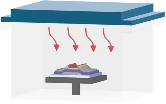
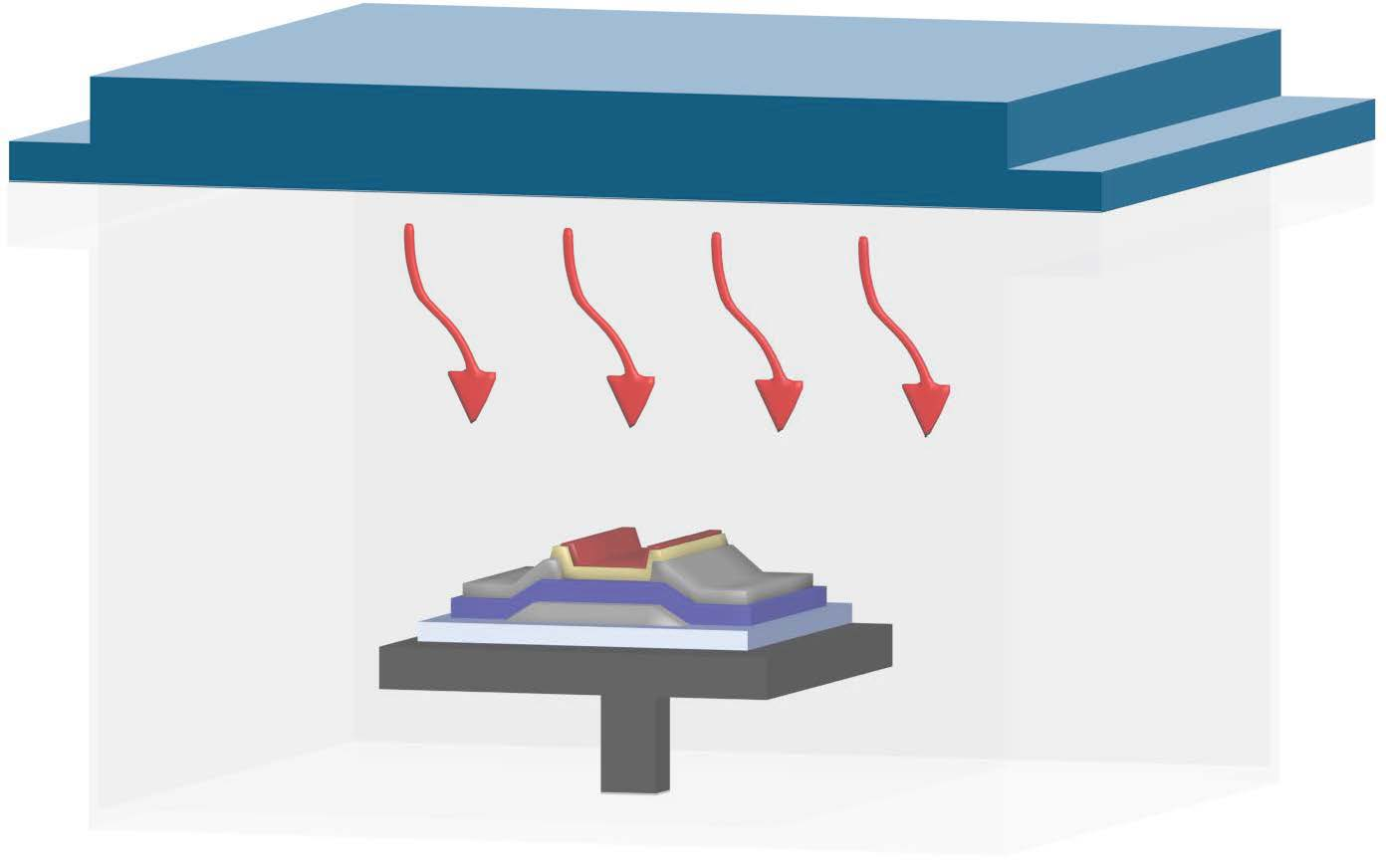
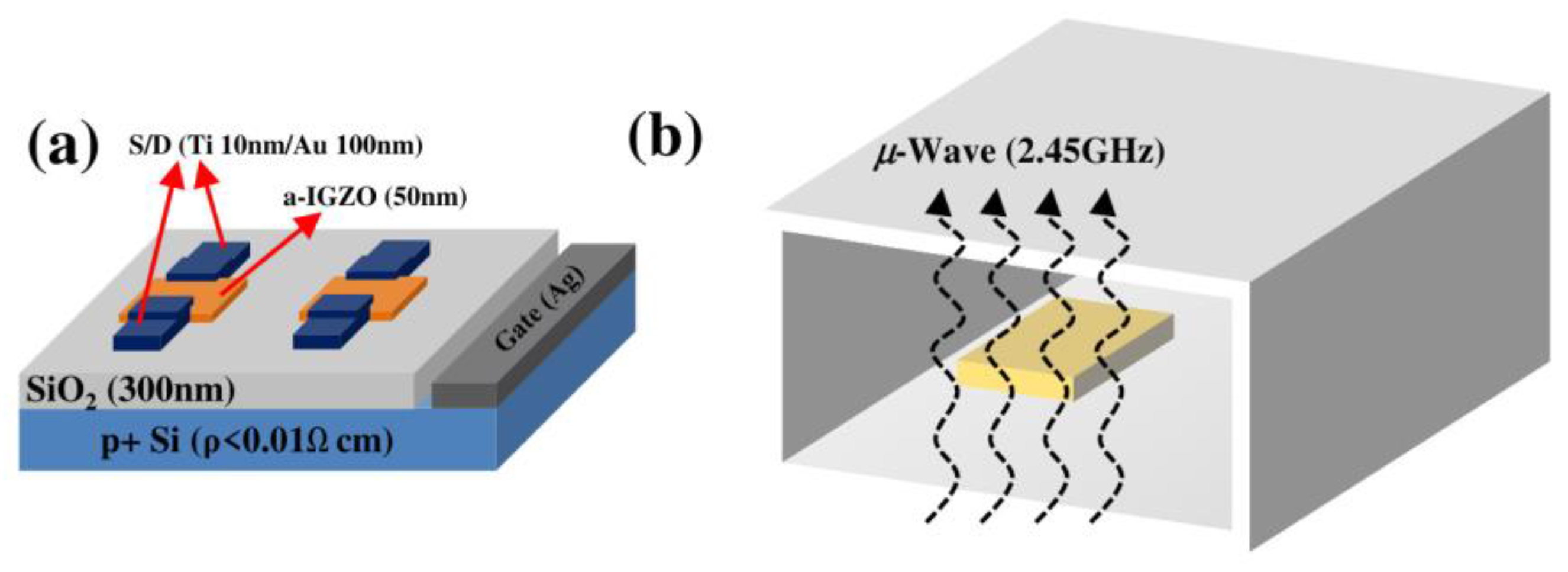
2. Experiment
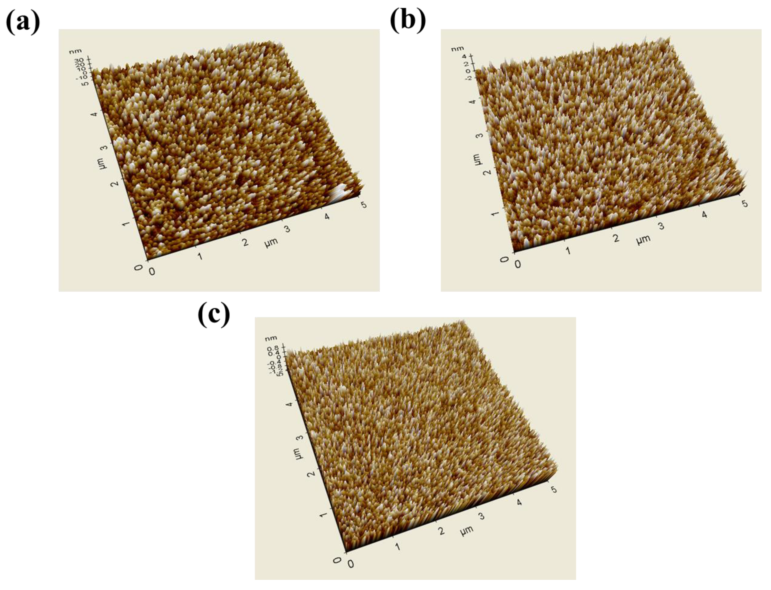
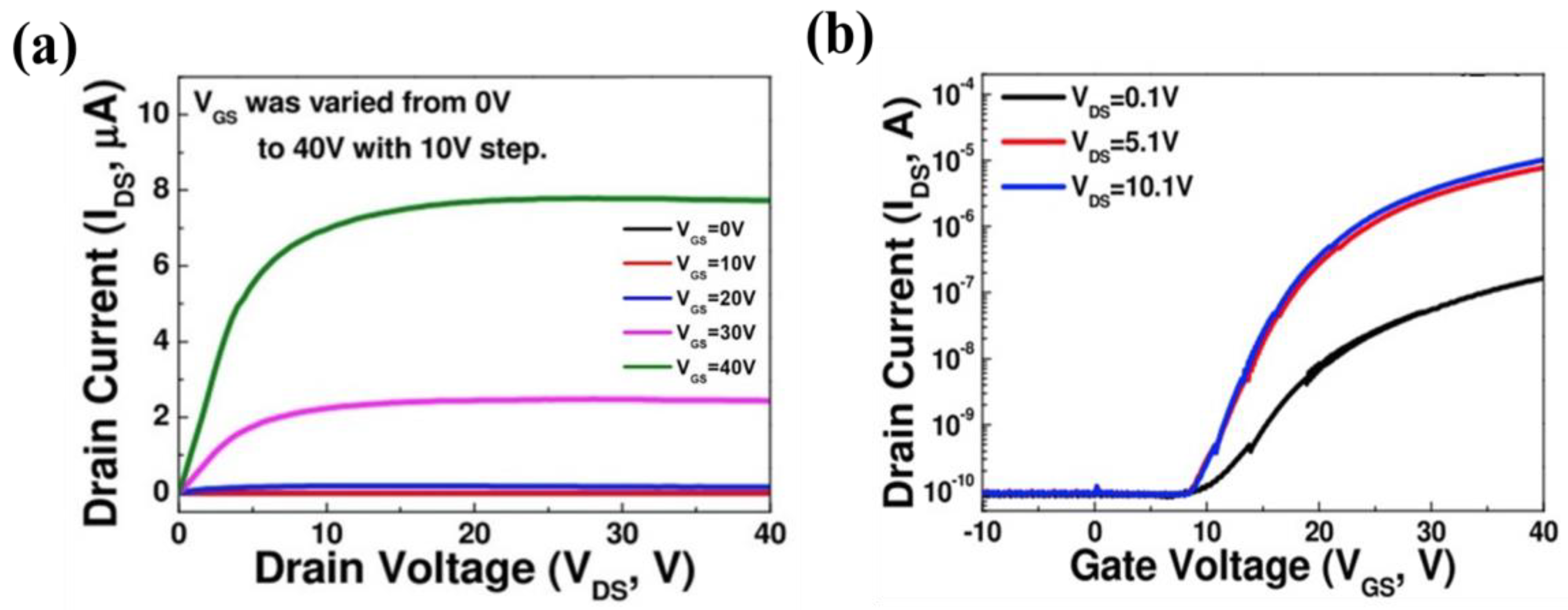
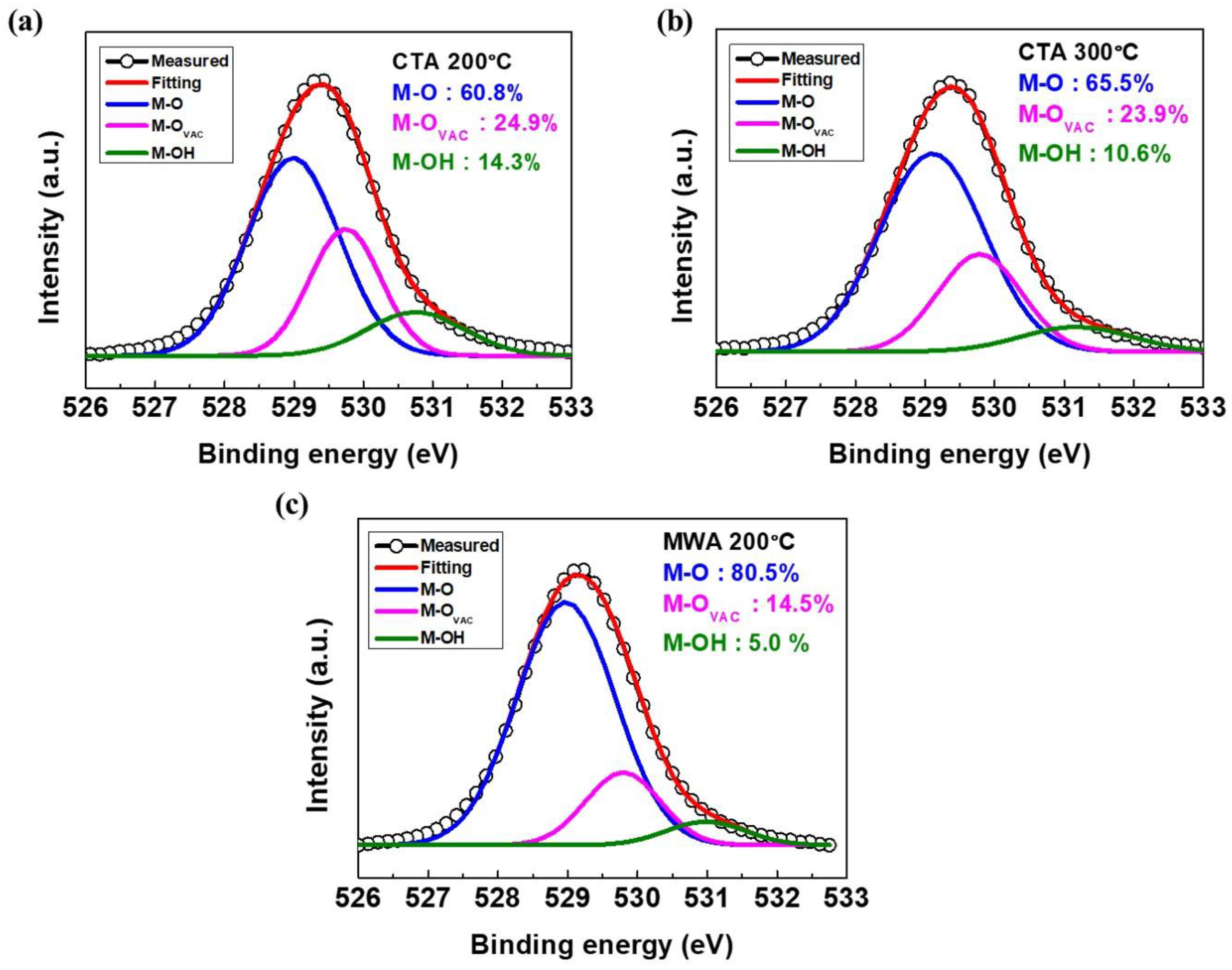
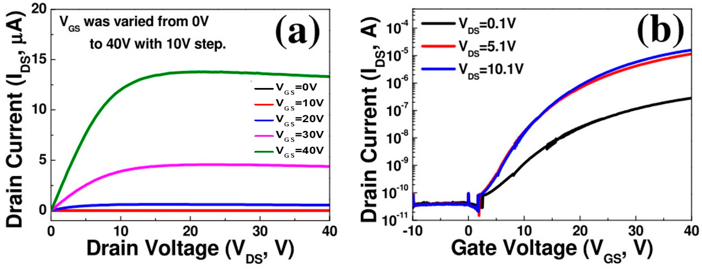
3. Results and Discussion
4. Conclusions
Author Contributions
Funding
Conflicts of Interest
References
- Street, R.A. (Ed.) Technology and Application of Amorphous Silicon; Springer: Berlin, Germany, 2000. [Google Scholar]
- Carcia, P.F.; McLean, R.S.; Reilly, M.H.; Nunes, G., Jr. Transparent ZnO thin-film transistor fabricated by rf magnetron sputtering. Appl. Phys. Lett. 2003, 82, 1117. [Google Scholar] [CrossRef]
- Nomura, K.; Ohta, H.; Takagi, A.; Kamiya, T.; Hirano, M.; Hosono, H. Room-temperature fabrication of transparent flexible thin-film transistors using amorphous oxide semiconductors. Nature 2004, 432, 488–492. [Google Scholar] [CrossRef] [PubMed]
- Song, J.-I.; Park, J.-S.; Kim, H.; Heo, Y.-W.; Lee, J.-H.; Kim, J.-J.; Kim, G.M.; Choi, B.D. Transparent amorphous indium zinc oxide thin-film transistors fabricated at room temperature. Appl. Phys. Lett. 2007, 90, 022106. [Google Scholar] [CrossRef]
- Jeong, J.K.; Jeong, J.H.; Yang, H.W.; Park, J.-S.; Mo, Y.-G.; Kim, H.D. High performance thin film transistors with cosputtered amorphous indium gallium zinc oxide channel. Appl. Phys. Lett. 2007, 91, 113505. [Google Scholar] [CrossRef]
- Park, J.-S.; Jeong, J.K.; Mo, Y.-G.; Kim, H.D.; Kim, S.-I. Improvements in the device characteristics of amorphous indium gallium zinc oxide thin-film transistors by Ar plasma treatment. Appl. Phys. Lett. 2007, 90, 262106. [Google Scholar] [CrossRef]
- Hosono, H.; Nomura, K.; Ogo, Y.; Uruga, T.; Kamiya, T. Factors controlling electron transport properties in transparent amorphous oxide semiconductors. J. Non-Cryst. Solids 2008, 354, 2796. [Google Scholar] [CrossRef]
- Barquinha, P.; Pereira, L.; Goncalves, G.; Martins, R.; Fortunato, E. The Effect of Deposition Conditions and Annealing on the Performance of High-Mobility GIZO TFTs. Electrochem. Solid-State Lett. 2008, 11, H248. [Google Scholar] [CrossRef]
- Liu, C.; Sun, Y.; Qin, H.; Liu, Y.; Wei, S.; Zhao, Y. Low-Temperature, High-Performance InGaZnO Thin-Film Transistors Fabricated by Capacitive Coupled Plasma-Assistant Magnetron Sputtering. IEEE Electron Device Lett. 2019, 40, 3. [Google Scholar] [CrossRef]
- Stanford, M.G.; Noh, J.H.; Mahady, K.; Levlev, A.V.; Maksymovych, P.; Ovchinnikova, O.S.; Rack, P.D. Room-Temperature Activation of InGaZnO Thin-Film Transistors via He+ Irradiation. ACS Appl. Mater. Interfaces 2017, 9, 35125–35132. [Google Scholar] [CrossRef] [PubMed]
- Zan, H.-W.; Chen, W.-T.; Chou, C.-W.; Tsai, C.-C.; Huang, C.-N.; Hsueh, H.-W. Low Temperature Annealing with Solid-State Laser or UV Lamp Irradiation on Amorphous IGZO Thin-Film Transistors. Electrochem 2010, 13, H1444. [Google Scholar] [CrossRef]
- Sheng, J.; Lee, H.-J.; Oh, S.; Park, J.-S. Flexible and high-performance amorphous indium zinc oxide thin-film transistor using low-temperature atomic layer deposition. ACS Appl. Mater. Interfaces 2016, 8, 33821–33828. [Google Scholar] [CrossRef] [PubMed]
- Park, J.W.; Kang, B.H.; Kim, H.J. A review of low-temperature solution-processed metal oxide thin-film transistors for flexible electronics. Adv. Funct. Mater. 2020, 30, 1904632. [Google Scholar] [CrossRef]
- Hur, J.S.; Kim, J.O.; Kim, H.A.; Jeong, J.K. Stretchable polymer gate dielectric by ultraviolet-assisted hafnium oxide doping at low temperature for high-performance indium gallium tin oxide transistors. ACS Appl. Mater. Interfaces 2019, 11, 21675–21685. [Google Scholar] [CrossRef]
- He, Y.; Wang, X.; Gao, Y.; Hou, Y.; Wan, Q. Oxide-based thin film transistors for flexible electronics. J. Semicond. 2018, 39, 011005. [Google Scholar] [CrossRef]
- Lee, G.J.; Kim, J.; Kim, J.-H.; Jeong, S.M.; Jang, J.E.; Jeong, J. High performance, transparent a-IGZO TFTs on a flexible thin glass substrate. Semicond. Sci. Technol. 2014, 29, 035003. [Google Scholar] [CrossRef]
- Gao, X.; Lin, L.; Liu, Y.; Huang, X. LTPS TFT process on polyimide substrate for flexible AMOLED. J. Disp. Technol. 2015, 11, 666–669. [Google Scholar] [CrossRef]
- Chang, S.; Dong, K.-Y.; Park, J.-H.; Oh, T.-Y.; Kim, J.-W.; Lee, S.; Ju, B.-K. Scaling down of amorphous indium gallium zinc oxide thin film transistors on the polyethersulfone substrate employing the protection layer of parylene-C for the large-scale integration. Appl. Phys. Lett. 2010, 96, 243504. [Google Scholar] [CrossRef]
- Bae, H.-S.; Kwon, J.-H.; Chang, S.; Chung, M.-H.; Oh, T.-Y.; Park, J.-H.; Lee, S.; Pak, J.J.; Ju, B.-K. The effect of annealing on amorphous indium gallium zinc oxide thin film transistors. Thin Solid Films 2010, 518, 6325–6329. [Google Scholar] [CrossRef]
- Haque, K.E. Microwave energy for mineral treatment processes—A brief review. Int. J. Miner. Process. 1999, 57, 1–24. [Google Scholar] [CrossRef]
- Rao, K.J.; Vaidhyanathan, B.; Ganguli, M.; Ramakrishnan, P.A. Synthesis of inorganic solids using microwaves. Chem. Mater. 1999, 11, 882–895. [Google Scholar] [CrossRef]
- Ahn, J.; Lee, J.; Kim, Y.; Ahn, B. Microwave-induced low-temperature crystallization of amorphous Si thin films. Curr. Appl. Phys. 2002, 2, 135–139. [Google Scholar] [CrossRef]
- Thostenson, E.T.; Chou, T.W. Microwave processing: Fundamentals and applications. Compos. Part A Appl. Sci. Manuf. 1999, 30, 1055–1071. [Google Scholar] [CrossRef]
- Jones, D.A.; Lelyveld, T.P.; Mavrofidis, S.D.; Kingman, S.W.; Miles, N.J. Microwave heating applications in environmental engineering—A. review. Resour. Conserv. Recycl. 2002, 34, 75–90. [Google Scholar] [CrossRef]
- Chung, H.-j.; Jeong, J.; Ahn, T.; Lee, H.; Kim, M.; Jun, K.; Park, J.-s.; Jeong, J.; Mo, Y.-g.; Kim, H. Bulk-limited current conduction in amorphous InGaZnO thin films. Electrochem. Solid-State Lett. 2007, 11, H51. [Google Scholar] [CrossRef]
- Greve, D. Field Effect Devices and Applications: Devices for Portable Low Power, and Imaging Systems; Prentice-Hall: Upper Saddle River, NJ, USA, 1988. [Google Scholar]
- Na, J.H.; Kitamura, M.; Arakawa, Y. High field-effect mobility amorphous InGaZnO transistors with aluminum electrodes. Appl. Phys. Lett. 2008, 93, 063501. [Google Scholar] [CrossRef]
- Bong, H.; Lee, W.; Lee, D.; Kim, B.; Cho, J.; Cho, K. High-mobility low-temperature ZnO transistors with low-voltage operation. Appl. Phys. Lett. 2010, 96, 192115. [Google Scholar] [CrossRef]
- Kim, I.; Choi, Y.; Tuller, H. Low-voltage ZnO thin-film transistors with high-K Bi1.5 Zn1.0 Nb1.5 O7 gate insulator for transparent and flexible electronics. Appl. Phys. Lett. 2005, 87, 043509. [Google Scholar] [CrossRef]
- Park, K.-W.; Cho, W.-J. Thermal damage-free microwave annealing with efficient energy conversion for fabricating of high-performance a-IGZO thin film transistors on flexible substrates. Materials 2021, 14, 2630. [Google Scholar] [CrossRef]
- Cheong, H.; Ogura, S.; Ushijima, H.; Yoshida, M.; Fukuda, N.; Uemura, S. Rapid preparation of solution-processed InGaZnO thin films by microwave annealing and photoirradiation. AIP Adv. 2015, 5, 067127. [Google Scholar] [CrossRef]
- Galesic, I.; Reusch, U.; Angelkort, C.; Lewalter, H.; Berendes, A.; Schweda, E.; Kolbesen, B.O. Nitridation of vanadium in molecular nitrogen: A comparison of rapid thermal processing (RTP) and conventional furnace annealing. Vacuum 2001, 61, 479–484. [Google Scholar] [CrossRef]
- Jeong, J.H.; Yang, H.W.; Park, J.-S.; Jeong, J.K.; Mo, Y.-G.; Kim, H.D.; Song, J.; Hwang, C.S. Origin of subthreshold swing improvement in amorphous indium gallium zinc oxide transistors. Electrochem. Solid-State Lett. 2008, 11, H157. [Google Scholar] [CrossRef]
- Fuh, C.-S.; Liu, P.-T.; Chou, Y.-T.; Teng, L.-F.; Sze, S.M. Role of oxygen in amorphous In-Ga-Zn-O thin film transistor for ambient stability. ECS J. Solid-State Sci. Technol. 2012, 2, Q1. [Google Scholar] [CrossRef]
- Lee, J.-M.; Cho, I.-T.; Lee, J.-H.; Kwon, H.-I. Bias-stress-induced stretched-exponential time dependence of threshold voltage shift in InGaZnO thin film transistors. Appl. Phys. Lett. 2008, 93, 093504. [Google Scholar] [CrossRef]
- Kollath, A.; Brezhneva, N.; Skorb, E.V.; Andreeva, D.V. Microbubbles trigger oscillation of crystal size in solids. Phys. Chem. Chem. Phys. 2017, 19, 6286–6291. [Google Scholar] [CrossRef] [PubMed]
- Zhang, L.; Belova-Margi, V.; Wang, H.; Dong, W.-F.; Moehwald, H. Controlled Cavitation at Nano/Microparticle Surfaces. Chem. Mater. 2014, 26, 2244–2248. [Google Scholar] [CrossRef]
- Fortunato, E.M.C.; Pereira, L.M.N.; Barquinha, P.M.C.; Botelho do Rego, A.M.; Gonçalves, G.; Vilà, A.; Morante, J.R.; Martins, R.F.P. High mobility indium free amorphous oxide thin film transistors. Appl. Phys. Lett. 2008, 92, 222103. [Google Scholar] [CrossRef]
- Kimerling, L.C.; Patel, J.R. Defect states associated with dislocations in silicon. Appl. Phys. Lett. 1979, 34, 73–75. [Google Scholar] [CrossRef]
- Hata, N.; Wagner, S. A comprehensive defect model for amorphous silicon. J. Appl. Phys. 1992, 72, 2857–2872. [Google Scholar] [CrossRef]
- Jang, S.C.; Park, J.; Kim, H.-D.; Hong, H.; Chung, K.-B.; Kim, Y.J.; Kim, H.-S. Low temperature activation of amorphous In-Ga-ZnO semiconductors using microwave and e-beam radiation, and the associated thin film transistor properties. AIP Adv. 2019, 9, 025204. [Google Scholar] [CrossRef]
- Cheng, H.-C.; Tsay, C.-Y. Flexible a-IZO thin film transistors fabricated by solution processes. J. Alloys Compd. 2010, 507, L1–L3. [Google Scholar] [CrossRef]
- Lee, I.-K.; Lee, K.H.; Cho, W.-J. Microwave annealing effect for highly reliable biosensor: Dual-gate ion-sensitive field-effect transistor using amorphous InGaZnO thin-film transistor. ACS Appl. Mater. Interfaces 2014, 6, 22680–22686. [Google Scholar] [CrossRef] [PubMed]


| Parameters | VTH (V) | ION/OFF | S.S (V/DEC) | MSAT (CM2/V·s) | Nd (cm−3) |
|---|---|---|---|---|---|
| THERMAL, 200 °C | 34.9 | 8.04 × 10³ | 8.813 | 0.12 | 3.32 × 10¹⁷ |
| THERMAL, 300 °C | 7.5 | 7.76 × 10⁵ | 2.74 | 6.06 | 3.23 × 10¹⁶ |
| M-WAVE, 200 °C | 13.9 | 1.14 × 10⁵ | 3.05 | 4.23 | 1.35 × 10¹⁷ |
Publisher’s Note: MDPI stays neutral with regard to jurisdictional claims in published maps and institutional affiliations. |
© 2022 by the authors. Licensee MDPI, Basel, Switzerland. This article is an open access article distributed under the terms and conditions of the Creative Commons Attribution (CC BY) license (https://creativecommons.org/licenses/by/4.0/).
Share and Cite
Kim, J.-W.; Park, S.-G.; Yang, M.K.; Ju, B.-K. Microwave-Assisted Annealing Method for Low-Temperature Fabrication of Amorphous Indium-Gallium-Zinc Oxide Thin-Film Transistors. Electronics 2022, 11, 3094. https://doi.org/10.3390/electronics11193094
Kim J-W, Park S-G, Yang MK, Ju B-K. Microwave-Assisted Annealing Method for Low-Temperature Fabrication of Amorphous Indium-Gallium-Zinc Oxide Thin-Film Transistors. Electronics. 2022; 11(19):3094. https://doi.org/10.3390/electronics11193094
Chicago/Turabian StyleKim, Jong-Woo, Seong-Geon Park, Min Kyu Yang, and Byeong-Kwon Ju. 2022. "Microwave-Assisted Annealing Method for Low-Temperature Fabrication of Amorphous Indium-Gallium-Zinc Oxide Thin-Film Transistors" Electronics 11, no. 19: 3094. https://doi.org/10.3390/electronics11193094
APA StyleKim, J.-W., Park, S.-G., Yang, M. K., & Ju, B.-K. (2022). Microwave-Assisted Annealing Method for Low-Temperature Fabrication of Amorphous Indium-Gallium-Zinc Oxide Thin-Film Transistors. Electronics, 11(19), 3094. https://doi.org/10.3390/electronics11193094