Article

Reset Noise Sampling Feedforward Technique (RNSF) for Low Noise MEMS Capacitive Accelerometer

1
School of Electronic Engineering, Xidian University, Xi’an 710071, China
2
School of Electronic Engineering, Xi’an University of Posts & Telecommunications, Xi’an 710121, China
*
Author to whom correspondence should be addressed.
Electronics 2022, 11(17), 2693; https://doi.org/10.3390/electronics11172693
Submission received: 4 August 2022 / Revised: 22 August 2022 / Accepted: 24 August 2022 / Published: 27 August 2022

Abstract

:
The reset noise sampling feedforward (RNSF) technique is proposed in this paper to reduce the noise floor of the readout circuit for micro-electromechanically systems (MEMS) capacitive accelerometer. Because of the technology-imposed size restriction on the sensing element, the sensing capacitance and the capacitance variation are reduced to the femto-farad level. As a result, the reset noise from the parasitic capacitance, which is pico-farad level, becomes significant. In this work, the RNSF technique focuses on the suppression of the parasitic-capacitance-induced noise, thereby improving the noise performance of MEMS capacitive accelerometer. The simulation results show that the RNSF technique effectively suppresses the thermal noise from the parasitic capacitance. Compared with the traditional readout circuit, the noise floor of the readout circuit with the RNSF technique is reduced by 9 dBV. The presented circuit based on the RNSF technique is fabricated by a commercial 0.18- μ m BCD process and tested with a femto-farad MEMS capacitive accelerometer. The physical measurement results show that, compared with the readout circuit without the RNSF technique, the RNSF technique reduces the noise floor of the readout circuit for MEMS capacitive accelerometer from −72 dBV to −80 dBV. Compared with other similar works, the proposed readout circuit achieves better F o M   ( F o M = ( p o w e r × n o i s e   f l o o r ) / s y s t e m   b a n d w i d t h = 490   μ W · μ g / Hz ) among the switched-capacitor readout circuits.

1. Introduction

Micro-electromechanical systems (MEMS) capacitive sensor is widely used in pressure sensors and accelerometers for health care applications [1,2,3] and internet of things (IoT) applications [4]. In these applications, the sensors are powered by a battery, thus high power efficiency is required to extend battery life [5,6]. As a result, the MEMS capacitive sensors are designed with open-loop architecture rather than a closed-loop one to achieve low power consumption. Because the closed-loop structure needs to provide feedback to the MEMS sensor in electrostatic force, a high voltage, larger than a few volts in most cases, should be used to generate the electrostatic force to move proof mass. It will lead to larger power consumption and high cost [7,8]. Compared to the closed-loop architecture, the open-loop architecture does not need high voltage to drive the MEMS sensor, which consumes less power at the cost of linearity. In the open-loop architecture, the nonlinearity of the mechanical sensing element significantly increases with the increase of the capacitance variation of the sensing element [9,10]. Therefore, the capacitance variation needs to be limited to the femto-farad level to suppress the nonlinearity to an acceptable level [11,12]. However, the fact that the capacitance variation of the sensing element (femto-farad level) is much lower than the capacitance of parasitic capacitance of the sensing element (pico-farad-level) results in significant deterioration of gain error and thermal noise [13,14,15].
The chopper stabilization (CHS) technique [16,17] and correlated double sampling (CDS) technique [18,19,20] can cancel the offset and 1/f noise of the amplifier, but they cannot reduce the effect of thermal noise. Current-reuse techniques are important techniques to enhance the trans-conductance of the amplifier and reduce the noise floor, which includes the inverter-based amplifier [21,22], inverter stacking amplifier [23], and orthogonal current reuse [24]. However, they do not deal with parasitic-capacitance-induced noise. The thermal noise canceling technique [25] and feedforward noise reduction technique [26] focuse on the suppression of the amplifier’s noise, they also cannot solve the problem of thermal noise deterioration caused by parasitic capacitance. The wideband feedback control can suppress the parasitic-induced noise by a negative feedback loop control, but the controlling mechanism is complex and consumes a lot of power. The oversampling method can deal with all the noise both from parasitic capacitance and amplifier. However, it leads to high power consumption and low power efficiency [27,28,29]. Modified correlated double sampling (CDS) can also deal with noise from parasitic capacitance [30,31,32]. However, it reduces the bandwidth and driving ability of the pre-amplifier and, therefore, reduces power efficiency. As a result, these methods are not sufficiently power-efficient. In this paper, the reset noise sampling feedforward (RNSF) technique is proposed for reducing the noise from the parasitic capacitance in an open-loop readout circuit for MEMS capacitive accelerometer. This technique employs the sample noise charge and feedforward cancellation method to suppress the thermal noise. The whole process of noise reduction is based on a passive switched-capacitor network, which only consists of passive devices, such as switches and capacitors. No additional power is consumed. Therefore, the technique can consume less power to achieve large noise performance improvement of MEMS capacitive accelerometer without sacrificing others’ performance. Compared to the methods mentioned above, this technique provides high power efficiency in terms of the figure of merit ( F o M ) and flexibility.
The rest of the paper is organized as follows. Section 2 provides the noise analysis of the traditional readout circuit of MEMS capacitive accelerometer. In Section 3, the principles of the RNSF technique and the noise performance of the readout circuit with the RNSF technique are described in detail. Besides, the comparison of RNSF and CDS is illustrated. In Section 4 and Section 5, the simulation results and physical measurement results are presented. The conclusions are then drawn in Section 6.

2. Noise Performance of Traditional Readout Circuit

For the open-loop readout circuit with significant input parasitic capacitance, the overall noise performance of the readout circuit and the trade-off between noise and power is determined by a front-end switched-capacitor capacitance-to-voltage converter (SC-CVC) rather than a back-end analog-to-digital converter (ADC). In this section, the sensor structure and SC-CVC noise performance are analyzed in detail.

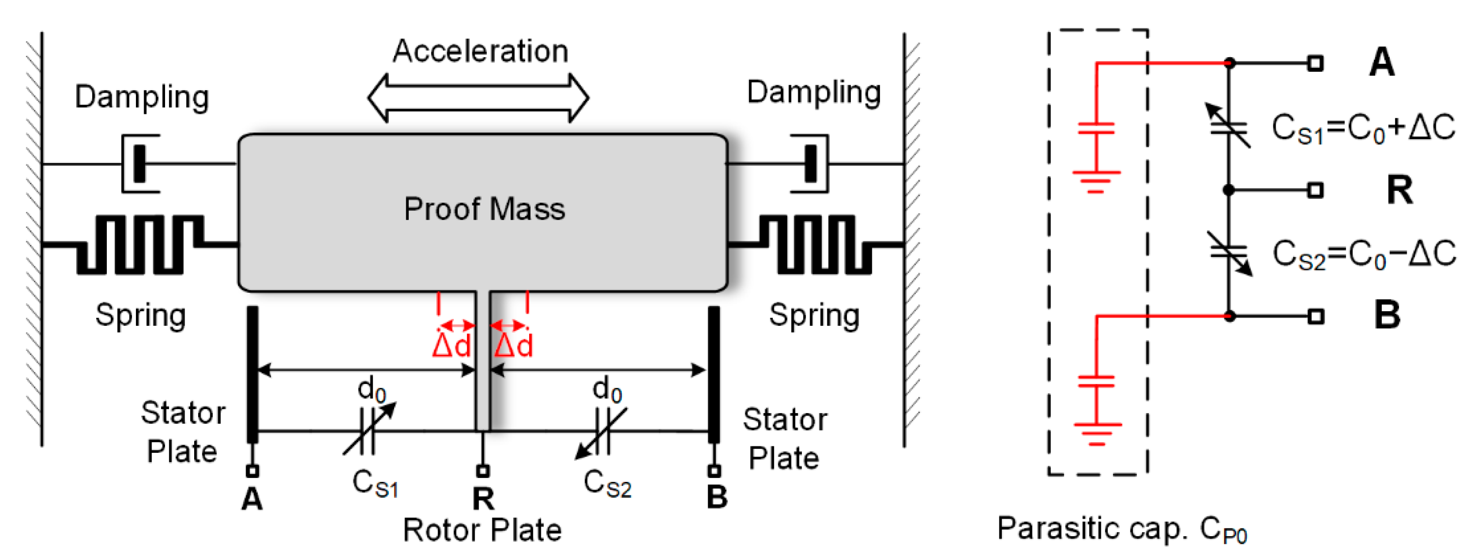
2.1. Sensor Structure

Figure 1 shows one sensing element in a typical open-loop MEMS capacitive accelerometer. The mechanical sensor consists of a moving proof mass suspended on springs over a substrate and a set of fixed electrodes. Applying external acceleration to the MEMS system leads to the deflection of the proof-mass from its center position, resulting in a differential capacitance change. The sensing capacitances C S 1 and C S 2 are the parallel-plate capacitors formed by the stator plates (unmovable plates connected to the sensing electrodes A and B) and the rotor plates (movable plates on the proof mass connected to the driving electrode R via spring), which are expressed below,
C S 1 = C 0 1 Δ d / d 0 C 0 ( 1 + Δ d d 0 ) = C 0 + Δ C , C S 2 = C 0 1 + Δ d / d 0 C 0 ( 1 Δ d d 0 ) = C 0 Δ C Δ C S = C S 1 C S 2 = 2 C 0 d 0 Δ d ( 1 1 ( Δ d / d 0 ) 2 ) n o n l i n e a r i t y   f a c t o r
where C 0 is the rest capacitance of the sensing capacitor, d 0 is the rest distance between a pair of rotor plates and stator plates which form the sensing capacitor, Δ d is the displacement which is in linear proportion to the acceleration signal. Equation (1) shows the capacitance variation of the differential parallel-plate capacitor ( Δ C S ) is a strongly nonlinear (reciprocal) function of displacement Δ d , which is undesirable for acceleration measurement. The normalized nonlinearity δ of differential capacitance variation   Δ C S is,
δ = | 1 1 1 ( Δ d / d 0 ) 2 | = ( Δ d / d 0 ) 2 1 ( Δ d / d 0 ) 2
According to Equation (2), in order to limit the high-order nonlinear approximation error to an acceptable level (e.g., δ < 0.1 % ), the maximum displacement ratio Δ d / d 0 should be less than 3.2%. For an acceptable MEMS die cost (e.g., 0.5 × 0.5   mm device fabricated by MEMS technology with an aspect ratio of 2/15 μ m , i.e., the minimum distance between the finger structures is 2 μ m and the maximum thickness of the finger structures is 15 μ m ), the sensor’s rest capacitance C 0 is about 250 fF [33,34], the maximum capacitance variation Δ C S will not exceed 8 fF to achieve 0.1 % nonlinearity.

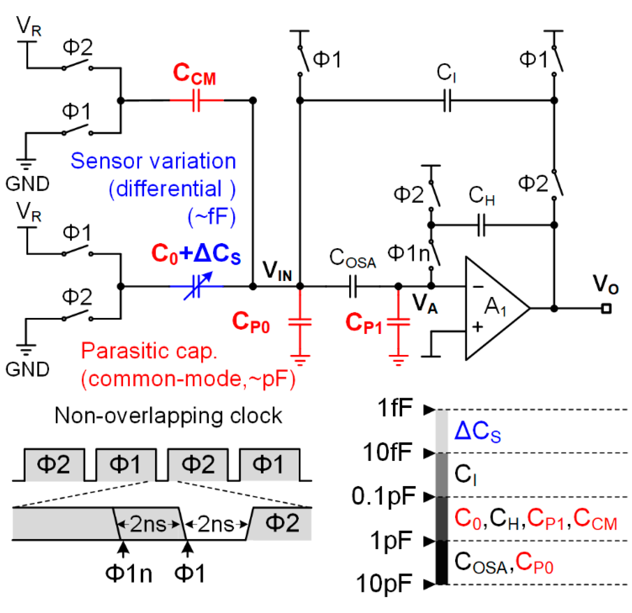
2.2. Noise Performance of Switched-Capacitor Capacitance-to-Voltage Converter

The simplified front-end single-end open-loop readout circuit of the femto-farad MEMS capacitive accelerometer is a switched-capacitor capacitance-to-voltage converter, as shown in Figure 2 [28].
The C P 0 is the parasitic capacitance between the sensing electrodes and the ground. It is introduced by MEMS sensor’s package, bonding pads, and electrostatic discharge protection (ESD) of IC chip. The   C P 1   is the parasitic capacitance introduced by the input transistors of the pre-amplifier   A 1 . The static capacitance C 0 of the sensing element is also modeled as the parasitic capacitance, as it does not contribute to any signal charge. The basic operation of SC-CVC is the sensing capacitance C S is excited by reference voltage   V R , the common-mode charge is absorbed by the capacitor   C C M , and only the differential signal charge flows into the integrating capacitor C I to produce an output voltage of SC-CVC.
V o u t = Δ C S C I V R = Δ C S G C V , G C V = V R C I
where G C V is sensitive/gain of the SC-CVC with a unit of V / F . The capacitors C O S A and C H are used to settle out gain error, offset, and 1/f noise.
The main noise source in the SC-CVC can be divided into two types. One is type-A noise due to reset noise sampled by the capacitors during phase Φ1 and amplified during phase Φ2. Type-A noise in the output voltage is [27],
V N A 2 ¯ = k T ( C C M + C P 0 + C P 1 + C 0 + C I ) C I 2 + k T C O S A 1 β 1 2 β 1 = C I C P 0 + C P 1 + C 0 + C I + C C M
where β 1 is the feedback coefficient from V O to V I N . The first term of Equation (4) represents charge-type noise from capacitances   C P 0 ,   C P 1 , C 0 , and C I . The second term of Equation (4) represents voltage-type noise from capacitor   C O S A .
The other one is type-B noise due to the amplifier A 1 during phase Φ2 when capacitor C H severing as load capacitor. Type-B noise in the output voltage is [31],
V N B 2 ¯ = 1 β 1 β 2 k T C H α γ ,     β 2 = C O S A C P 1 + C O S A
where β 2 is the feedback coefficient from V I N to V A , α is a constant depending on the structure of the input stage of amplifier A 1 with a typical value between 1.0 and 2.0, γ is a constant depending on the process with a typical value of 0.6.
The total equivalent input noise C I N 2 ¯ in the sensing capacitor is,
C I N 2 ¯ = ( V N A 2 ¯ + V N B 2 ¯ ) / G C V 2
The typical transient output noise waveform of SC-CVC is shown in Figure 3. The discrete-time random fluctuation between each period is type-A noise. The continuous-time random fluctuation in each period is type-B noise.
For the femto-farad-level MEMS capacitive accelerometer, the type-A noise induced by parasitic capacitance is larger than the type-B noise, then it becomes the dominant noise source. Combining Equations (4) and (5), the condition for type-A noise dominance can be acquired,
V N A 2 ¯ > V N B 2 ¯ C I C H < C P 0 + C P 1 + 2 C 0 + C O S A C O S A α γ
Equation (7) gives the threshold value of ratio C I / C H when type-A noise achieves dominance. Typically, the value of capacitance C P 0 is in the order of a few pico-farads. It is introduced by the MEMS device (600 fF), electrostatic discharge protector (1.2 pF), and bonding pad (200 fF). The value of capacitance C H and C O S A is also in the order of pico-farad, which provide the large loop gain to compensate for the finite gain error of the amplifier. The integrating capacitance C I should match the capacitance variation   Δ C S to ensure enough gain of the SC-CVC. Therefore, the value of capacitance C I is in the order of tens of femto-farads. Based on the values above, the condition for type-A noise dominance is easily satisfied. The variation of equivalent input noise with ratio C I / C H is shown in Figure 4. According to Equation (6), the type-B equivalent input noise decreases with decreasing of the ratio   C I / C H , while type-A equivalent input noise keeps constant. As a result, the total equivalent input noise is dominated by type-B noise with high ratio C I / C H (corresponding to pico-farad-level MEMS capacitive sensor) and dominated by type-A noise with low ratio C I / C H (corresponding to the femto-farad-level MEMS capacitive sensor).
In summary, the noise floor of the femto-farad-level MEMS capacitive readout circuit is dominated by the parasitic-capacitance-induced noise not by the operational amplifier (op-amp) noise.

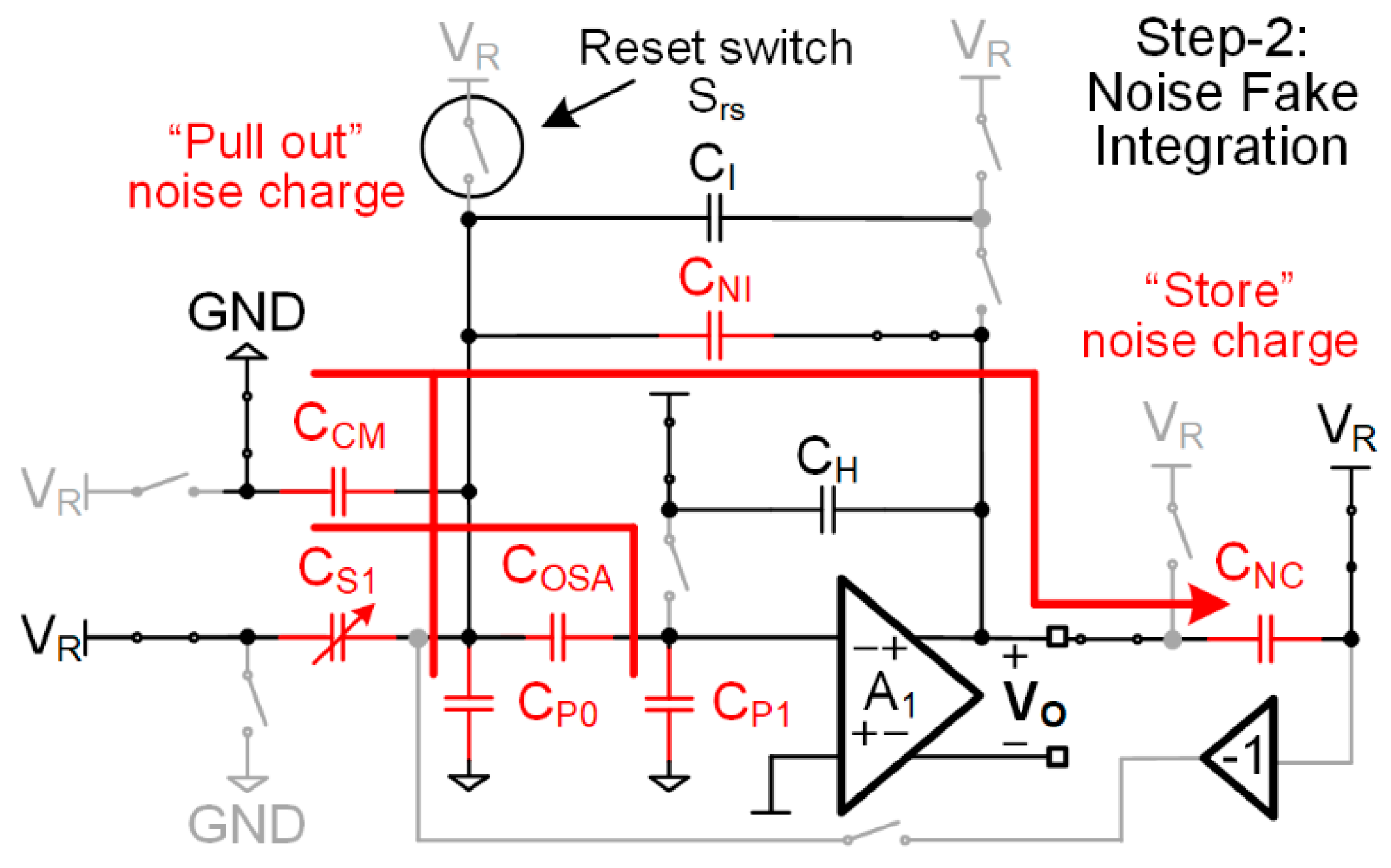
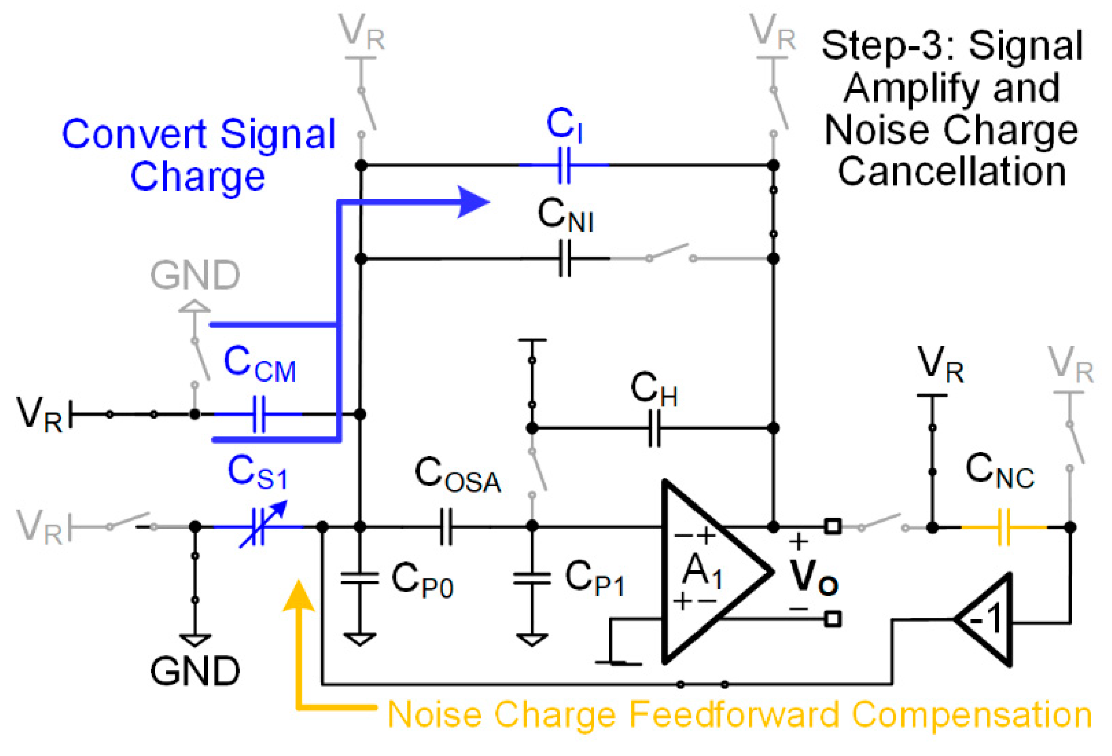
3. Reset Noise Sampling Feedforward (RNSF) Technique

As analyzed in Section 2, to improve the noise performance of the femto-farad-level MEMS capacitive readout circuit, suppressing type-A noise is more effective than suppressing type-B noise. Therefore, this work proposes a reset noise sampling feedforward (RNSF) technique that forces the suppression of the noise from the parasitic capacitance in an open-loop readout structure for the MEMS capacitive accelerometer.

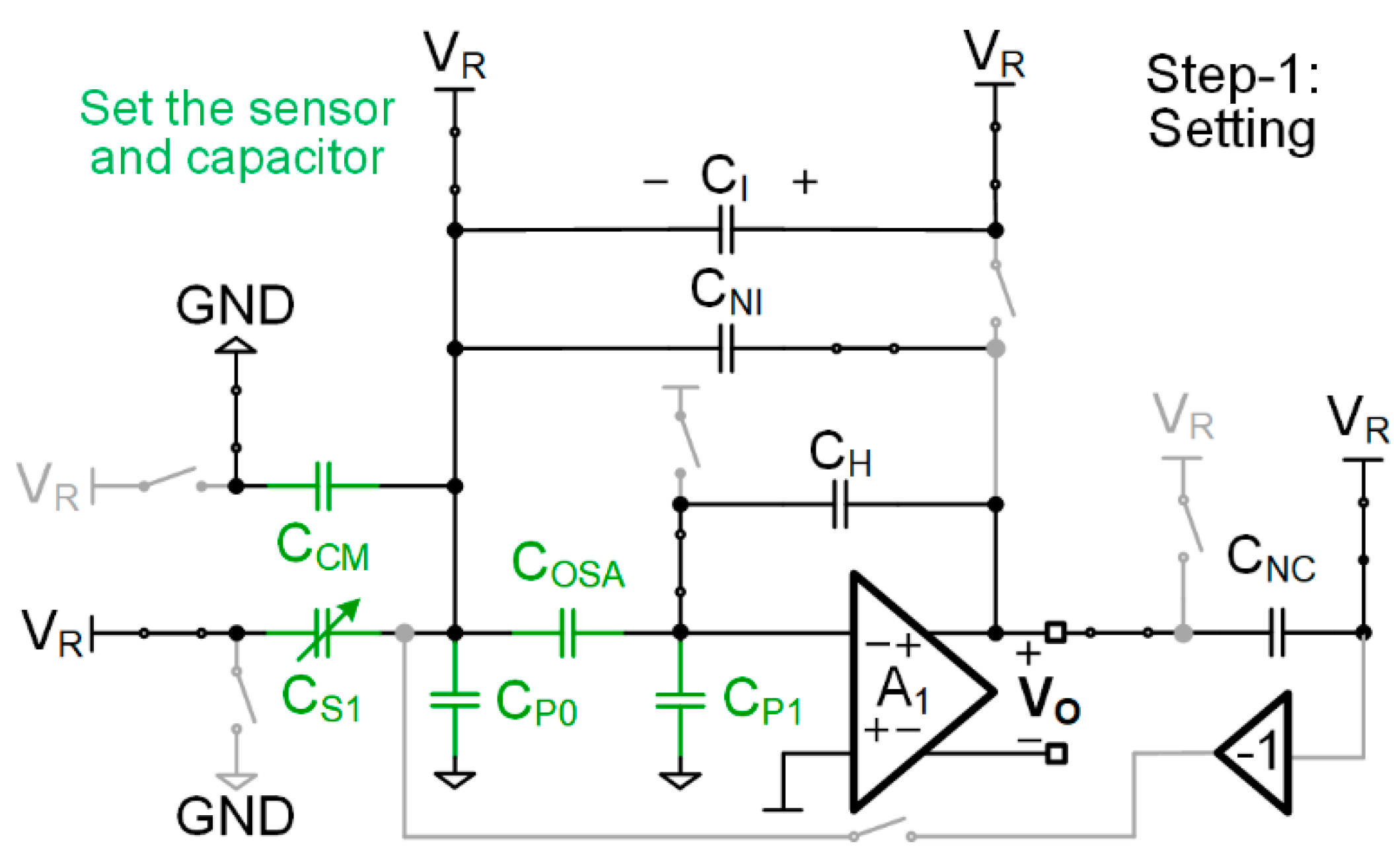
3.1. Circuit Implementation

The CVC employing RNSF technique does not change the topology structure, as the schematic and time diagram shown in Figure 5a. The main amplifier A 1 used in CVC is a fully differential two-stage amplifier, which is shown in Figure 5b. The switched-capacitor common-mode feedback (SC-CMFB) is used to control the output common-mode voltage without sacrificing extra power consumption. The generator of the non-overlapping clock is shown in Figure 5c. It is capable of generating three-phase non-overlapping clocks. Each clock has its own independent rising edge delay and falling edge delay. This generator can also produce nested clocks by cascading, and these clocks are used to drive the key switches, which reduce the effect of charge injection and clock feedthrough.

3.2. Principle

The RNSF technique works in three steps to settle out the type-A noise, as the single-end model shown in Figure 6, Figure 7 and Figure 8.
In step-1, the capacitors C S 1 , C O S A , C P 0 , C C M , and C P 1 in the circuit are reset, as shown in Figure 6. In this step, these capacitors are also charged with thermal noise. Notice that capacitor C N I , which stores the output voltage of last period V O ( n 1 ) , is not reset. The total noise charge sampled by these capacitors is
Q N C 2 = K T ( C C M + C P 0 + C P 1 + C S 1 + C I ) = K T C P _ t o t a l
In step-2, the reset switch S r s is open, then the sample noise on the parasitic capacitance C P _ t o t a l is frozen. The noise integration capacitor C N I is connected to execute a “noise fake integration” without driving the sensing capacitors   C S 1 . During “noise fake integration”, only the thermal noise charges flow into C N I while the signal charge does not, since the sensor capacitors are not driven, as shown in Figure 7. This operation separates the noise charge from the signal charge, as the capacitor C N I “pulls out” the noise charges from all the capacitances ( C S 1 , C O S A , C P 0 , and C P 1 ) simultaneously. These noise charges are stored by the capacitor C N C . Furthermore, this operation avoids the introduction of gain error. A slewing of output Δ V O will introduce a virtual ground error Δ V O / A 1 across the input terminals of amplifier A 1 . The virtual ground error is then amplified by a coefficient of 1 / β , which is significant due to parasitic capacitance according to Equation (3). This results in a significant gain error. Thus, the slewing of output Δ V O should be minimized to avoid gain error in CVC. During step-1 and step-2 of RNSF operation, as capacitor C N I holds the output voltage of last period   V O ( n 1 ) , the slewing of output is minimized, and so is the gain error.
In step-3, the capacitor C I is connected to execute signal amplifying, and the capacitor C N C builds the feedforward path to cancel the noise charge. The inverter block represents the polarity of the stored noise charge that needs to be reversed. It can be achieved by output signal cross-coupled in a fully differential structure. The sensing capacitors are driven, and the signal charge flows into capacitor C I to produce output voltage V O ( n ) , as shown in Figure 8. The stored noise charge is transferred to the virtual ground node through a feedforward path and neutralizes the noise charge on the parasitic capacitance. The dominant type-A noise charge is depleted in this step, output voltage in this step can achieve lower noise. The residual noise charge on parasitic capacitance is
Q N C 2 = K T ( C C M + C P 0 + C P 1 + C S 1 + C I ) = K T C P _ t o t a l
where the V N 2 is the equivalent input noise of the amplifier and the B W is the bandwidth of the amplifier.

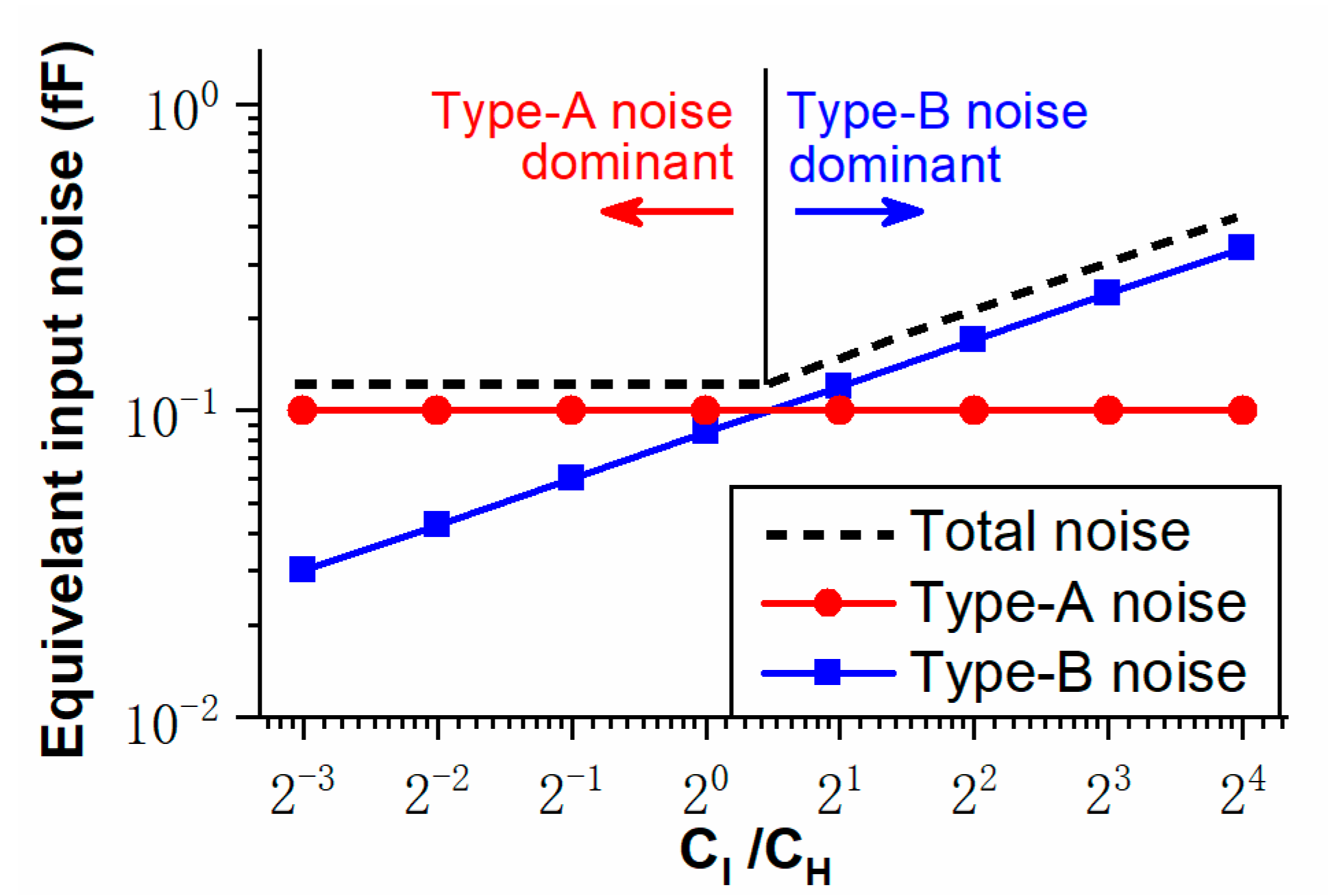
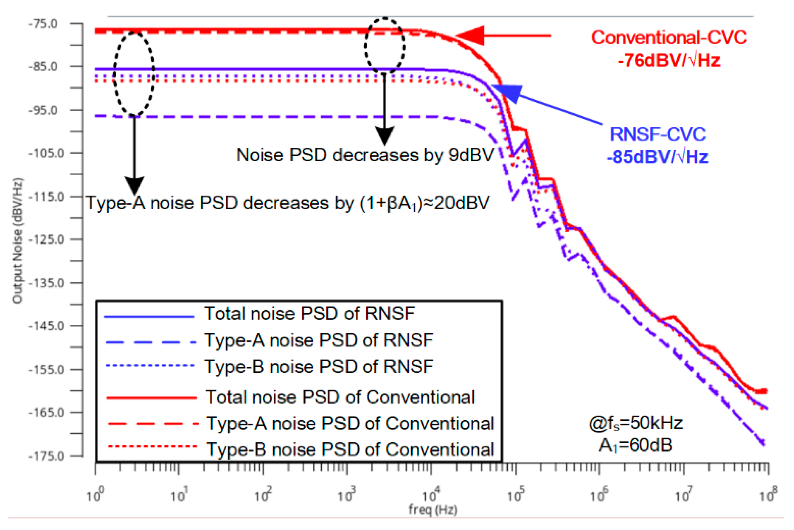
3.3. Noise Performance Analysis

The output noise of the RNSF-CVC is composed of three components. The first component is the reduced type-A noise. The second component is newly added noise when the amplifier settles out type-A noise. The third component is type-B noise, which remains unchanged.
The type-A noise in the capacitors C S 1 , C S 2 , C C M , C O S A , C P 0 , and C P 1 is pulled out by the amplifier through the capacitor C N I in phase Φ2 and is canceled by the feedforward compensation technique through the capacitor C N C in phase Φ3. Thus, the residual type-A noise V N A R 1 2 ¯ depends on the gain error of the amplifier, i.e.,
V N A R 1 2 ¯ = V N A 2 ¯   ( 1 1 + β 3 A 1 ) 2 , β 3 = C N I C N I + C P _ t o t a l
When the amplifier settles out type-A noise in the capacitors, it also introduces a new component of noise power V N A R 2 2 ¯ to those capacitors. This noise is actually a sampled noise of type-B noise in phase Φ2,
V N A R 2 2 ¯ = 1 β 3 k T C H α γ
During the whole RNSF process, type-B noise in phase Φ3 is unchanged. Thus, the total output noise of RNSF readout circuit is,
V N _ t o t a l 2 ¯ = V N A R 1 2 ¯ + V N A R 2 2 ¯ + V N B 2 ¯
The total equivalent input noise C I N 2 ¯ in the sensing capacitor is,
C I N 2 ¯ = ( V N A R 1 2 ¯ + V N A R 2 2 ¯ + V N B 2 ¯ ) / G C V 2
Compared with Equations (3) and (4) of the original CVC, Equation (9) indicates that the RNSF-CVC reduces type-A noise by a factor of ( 1 + β 2 A 1 ) 2 but increases extra type-B noise in phase Φ2. Thus, the RNSF technique can improve the noise performance if type-A noise is dominant. On the contrast, the RNSF technique will deteriorate the noise performance if type-B noise is dominant.

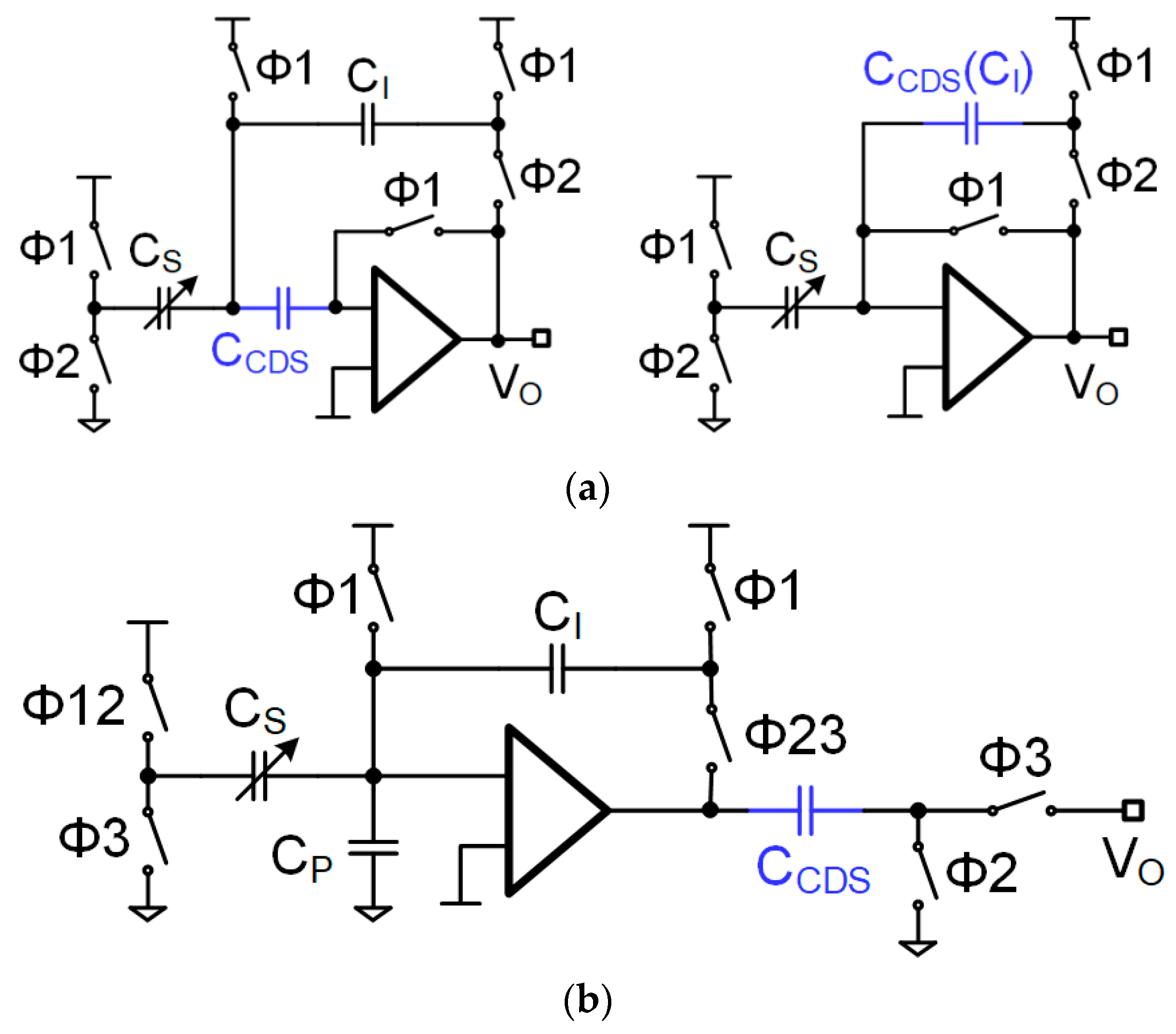
3.4. Noise Performance Comparison between RNSF and CDS

The various reported correlated double sampling (CDS) techniques can be divided into three types, as shown in Figure 9. Type-I CDS places the calibration capacitor C C D S in the front-end, so that the capacitor C C D S can sample the offset and flicker noise of the amplifier during phase Φ1 and cancel the offset and flicker noise during phase Φ2. However, the insertion of C C D S at the input terminal of the amplifier will introduce additional thermal noise. Type-II CDS uses the integration capacitor C I as a calibration capacitor, so that the capacitor C I can sample and cancel offset and flicker noise of the amplifier without introducing additional thermal noise. Type-III CDS places the calibration capacitor C C D S in the back-end. When driven in three phases, capacitor C C D S can sample and cancel not only the offset and flicker noise from the amplifier, but also sampled thermal noise (type-A noise) from sensing capacitor C S and parasitic capacitance C P . Thus, type-III CDS is most similar to the RNSF technique.
In type-III CDS technique shown in Figure 9b, two sampling phases are used to reduce type-A noise. During the first sampling phase Φ2, only noise is sampled by capacitor C C D S . During the second sampling phase Φ3, noise and signal are simultaneously sampled. As the noise is type-A noise which is correlated in two sampling phases’ Φ2 and Φ3, it can be canceled. However, capacitor C C D S reduces the bandwidth of the amplifier during phase Φ2 as it acts as load capacitor and reduces the driving ability of amplifier during phase Φ3 as it increases output impedance of the amplifier.
Compared with type-III CDS technique, the RNSF technique adopts the noise charge sample and feedforward cancelation method, which avoids the CDS capacitor acting as a load capacitor. Therefore, the bandwidth and driving ability of the amplifier are not sacrificed. Besides, the slewing of output is avoided, and gain error is minimized.
The comparison of three types of the CDS technique and CDA technique is summarized in Table 1. Type-II CDS is listed as reference. The symbol “+”, “O” and “−” represents better than the reference, the same as the reference and worse than the reference, respectively.

3.5. Drawbacks of RNSF Technique

Compared to the conventional SC-CVC structure, the sacrifice for the RNSF-CVC is the increasing of the clock phase by one and the chip area. The increase of clock phase will lead to the increase of settling error when the sampling frequency does not change. In order to reduce the settling error, a larger bandwidth of the operational amplifier is required, which means more power will be consumed. The relationship between the settling error, bandwidth, and sampling frequency is shown by the following equation:
e B W N × f s s e t t l i n g   e r r o r
where B W represents the bandwidth, the N represents the number of clock phase used, f s represents the sampling frequency. For example, to support a conventional SC-CVC (two clock phases) operating at 100 kHz sampling frequency with 1% settling error, the bandwidth should be at least 921 kHz, according to Equation (13). However, RNSF-CVC (three clock phases) needs a bandwidth of 1.38 MHz under the same condition.
The equivalent circuit model with typical component parameters of CVC is shown in Figure 10, the bandwidth of the CVC can be expressed as follows:
B W = β 1 β 2 g m 2 π C H
where g m is transconductance of the operational amplifier, the coefficient β 1 and β 2 is shown in Section 2.2. The value of the product of coefficient β 1 β 2 is about 0.017. For the SC-CVC with 921 kHz bandwidth, the g m should be 170 μ s which requires a typical supply current I D of 17 μ A . For the RNSF-CVC with 1.38 Mhz bandwidth, the g m should be 255 μ s , which requires 25 μ A supply current. Although the power consumption of RNSF-CVC is increased, the effect of noise suppression caused by RNSF-technique is excellent compared to other noise reduction techniques that consume the same power. Thus, for a fair comparison, the F o M is used to evaluate the performance of various noise reduction techniques. This content will be illustrated in Section 5.
Besides, compared to the whole area of the CVC, the increase of chip area introduced by RNSF technique can be negligible. Because the size of noise integration capacitor C N I , noise cancelation capacitor C N C is small, it will not occupy much more area of the chip. The switches used in CVC are designed by the MOS with the minimum lengths, thus the size of the switch is small. As a result, the RNSF network will not add more area.

4. Simulation Results

The CVC based on conventional and RNSF technique is simulated at the transistor level using the Periodic Steady State Analysis (PSS) tool in a fully differential capacitive readout circuit. The process is a commercial 0.18- μ m BCD process. The important conditions are   C I = 20   fF , C P 0 = 2   pF , C P 1 = 0.3   pF , C O S A = 4   pF , C H = 1   pF , C C M = C 0 = 0.3   pF ,   C N I = 20   fF , C N C = 20   fF , f S = 100   kHz .
The typical transient output waveform is shown in Figure 11, where the fine red line is the output of RNSF-CVC, the thick blue line is the output sampled during phase Φ3. The RNSF-CVC outputs significant noise in phase Φ2, as “noise fake integration” is executed in this phase. Then, RNSF-CVC outputs low noise signal in phase Φ3, as type-A noise charge from all the capacitors is settled out during phase Φ3. If the output is sampled in phase Φ3, the low noise output can be acquired. The noise power spectral density (PSD) of the RNSF-CVC and conventional CVC are shown in Figure 12. Due to the effect of RNSF technique, type-A noise PSD of RNSF is decreased by a factor of   ( 1 + β 2 A 1 ) , so the blue dash line is much lower than the red dash line. The total noise PSD of the RNSF-CVC decreases 9 dBV compared to the conventional CVC.
The results in Figure 13 show the noise reduction effectiveness of the RNSF technique varying with the parasitic capacitance C P 0 . When the value of C P 0 is increased from 0 to 5   pF , the equivalent input noise of traditional CVC without RNSF increases by 15   dBfF from 30   dBfF to 15   dBfF , while that of RNSF-CVC increases by only 10   dBfF from 38   dBfF to 28   dBfF . The RNSF-CVC not only significantly reduces the noise introduced by parasitic capacitance, it is also less sensitive to the increasing of parasitic capacitance.

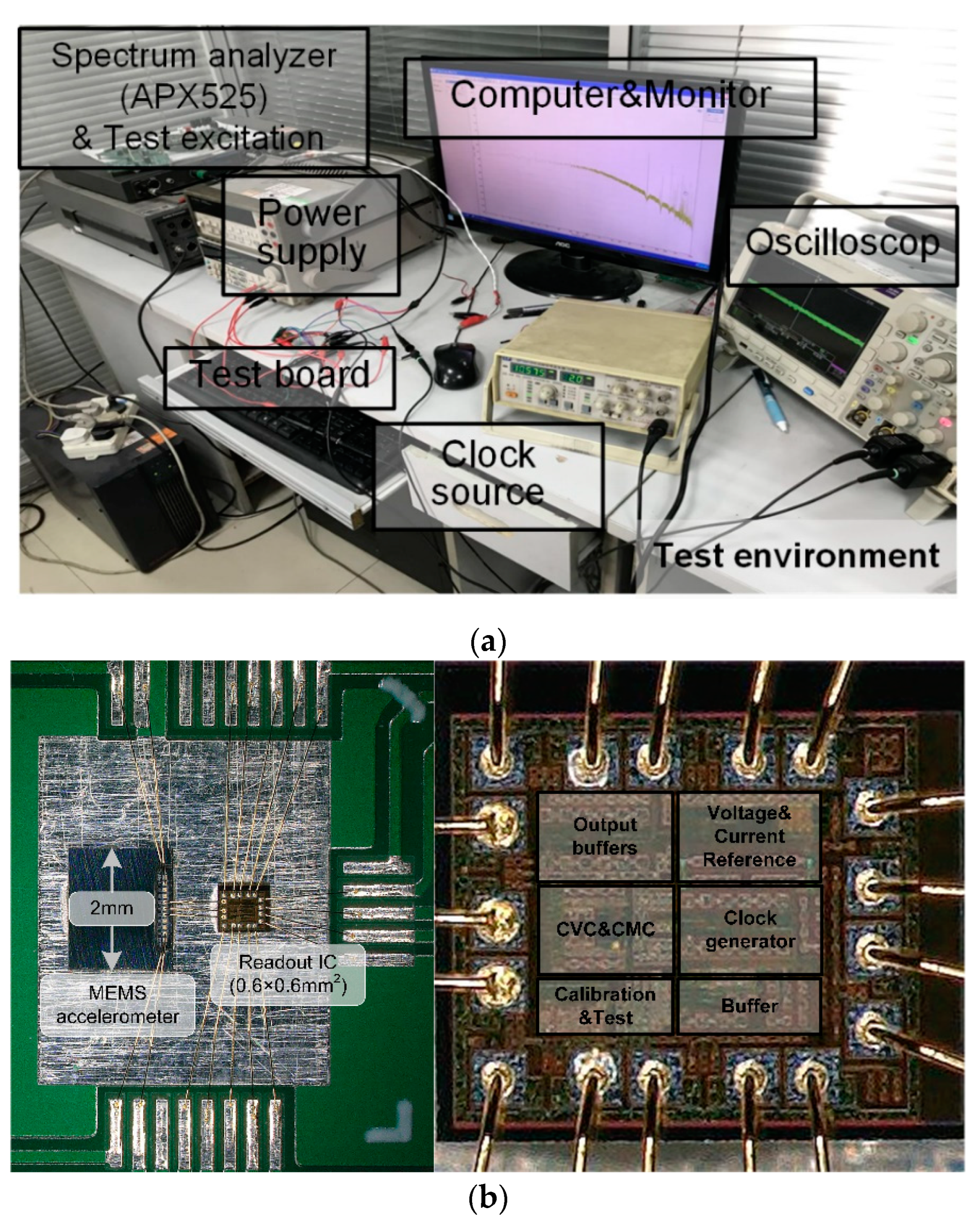
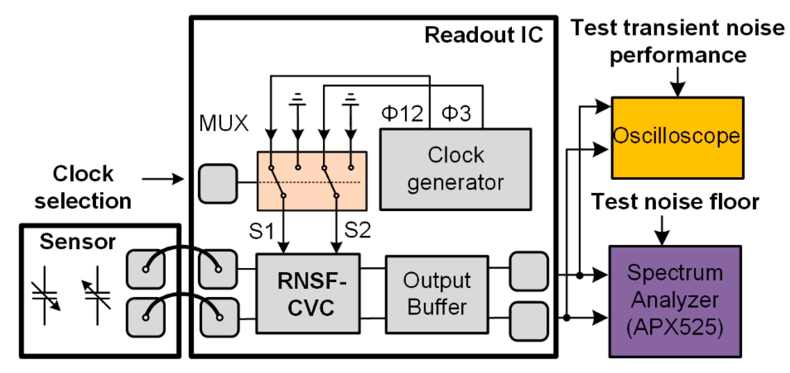
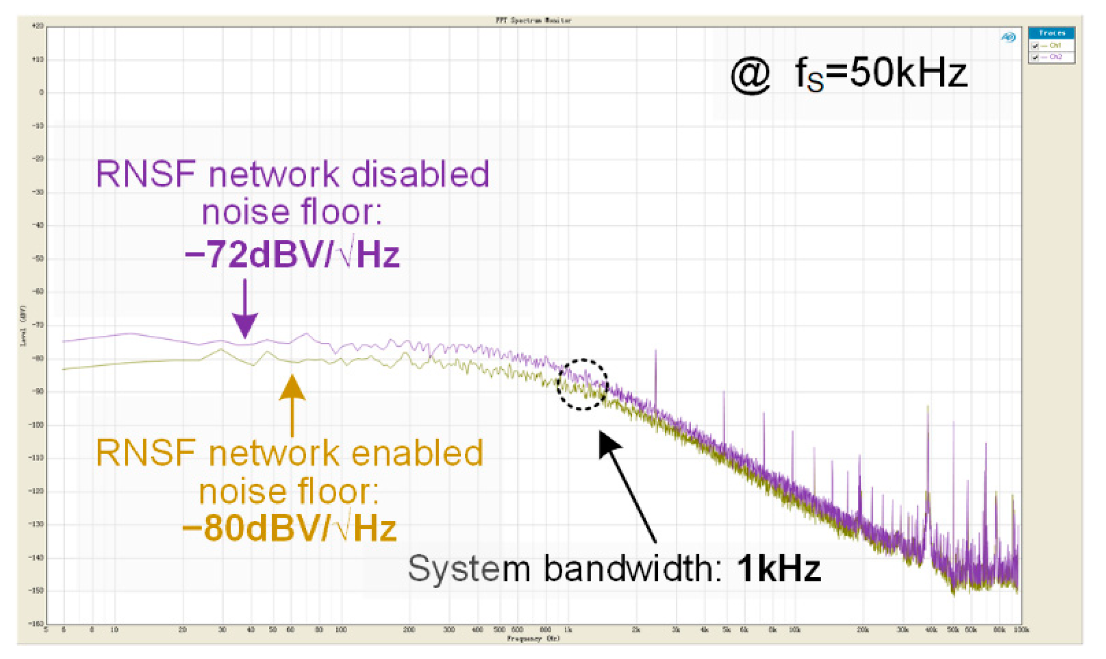
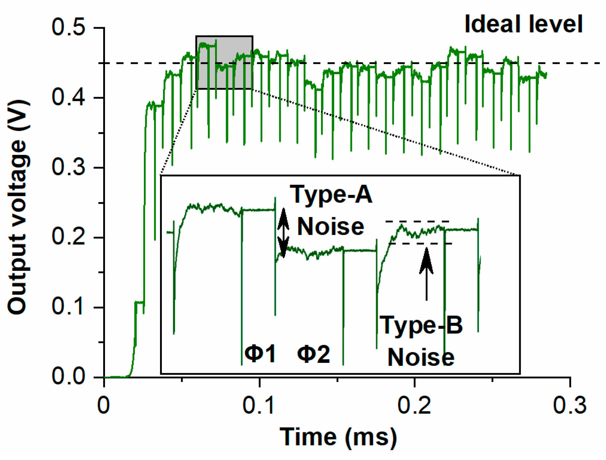
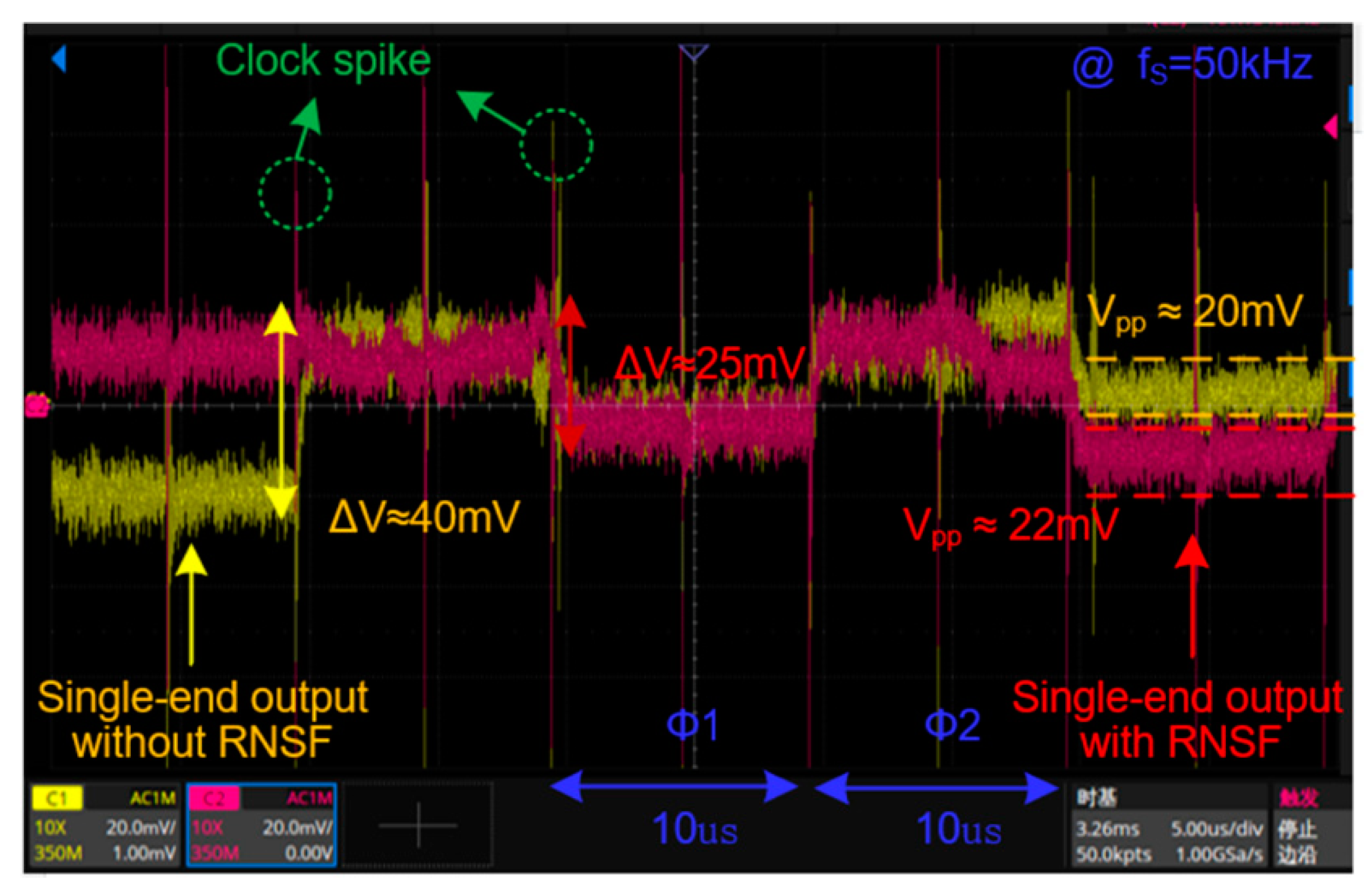
5. Physical Verification

The RNSF technique is verified in an open-loop structure readout circuit and tested with a commercial femto-farad MEMS accelerometer [35], as shown in Figure 14b. The typical parameters of the MEMS accelerometer are summarized in Table 2. The device size and the capacitive gap are 0.5 × 0.7 mm and 2.2 μ m , respectively. The thickness of the sensing element is 17   μ m and the proof mass is 3.5 μ g . The resonance frequency of the sensing element is about 2 kHz. The static capacitance is about 550 fF which is the sensor’s capacitance without any acceleration applied to it. The sensitivity of the MEMS capacitive accelerometer is 4 fF/g.
The readout circuit is manufactured with a commercial 0.18- μ m CMOS process, which integrates CMC (common-mode charge controller), CVC, calibration module, references, clock generator, and output buffers, as the micrograph of the die shown in Figure 14b. The CMC (common-mode charge controller) is used to absorb the common-mode charges from sensing capacitances so that only differential charge representing signal flows into the CVC to produce output voltage. The schematic of active CMC can be found in [36]. The calibration module is used to cancel the capacitive offset (typically in the order of 10 fF) introduced by a mismatch of MEMS sensing capacitors and bonding wires. The power consumption of the main blocks is 62 µW, where CMC, CVC, reference and clock generator consumes 20 µW, 30 µW, 10 µW, and 2 µW, respectively. The chip area.
To test the noise reduction ability of RNSF technique, a clock selector is added, which is shown in Figure 15. The clock selector provides two sets of clocks to drive switches S1 and S2 of CVC in Figure 3. When switches S1 and S2 are opened, the SC-CVC acts as a traditional CVC, as it does not execute “noise fake integration” during phase Φ2 and “noise charge compensation” during phase Φ3. When switches S1 and S2 are closed, the CVC obtains noise reduction ability. The output of CVC is connected to the oscilloscope and spectrum analyzer (APX525) to test the transient noise performance and the noise floor of the readout circuit.
The measurement results of transient noise performance are shown in Figure 16. When the RNSF technique is disabled, the output random fluctuation of CVC between each period is about 40 mV (the yellow line). When the RNSF technique is enabled, the output random fluctuation of CVC between each period is reduced to 25 mV (the red line). It means the type-A noise is effectively suppressed by RNSF technique. The peak-to-peak noise output in the period of these two outputs are similar because the RNSF technique cannot deal with the type-B noise, which is the amplifier’s noise.
The measurement results of the noise floor are shown in Figure 17. When the RNSF function is disabled, the output noise power spectral density is −72 dBV/√Hz with 1 kHz bandwidth. When the RNSF function is enabled, the output noise power spectral density is significantly reduced from −72 dBV/√Hz to −80 dBV/√Hz. The noise floor of the CVC is reduced due to the suppression of type-A noise. Therefore, this result verifies the effectiveness of the RNSF technique.
Generally, the figure of merit ( F o M ) is used to evaluate the power efficiency of MEMS accelerometer,
F o M   [ W · F / H z ] = P o w e r × N o i s e   f l o o r B w
The   F o M emphasizes the current efficiency, i.e., to reduce the noise floor with as little increment of supply current as possible.
The main experimental parameters of this work are listed in Table 3. This work reduces the noise floor from 627 to 250 ug/√Hz due to RNSF operation without sacrificing more power consumption. Compared to the previous work on OSA readout structure using a similar sensing element [28], this work achieves 11 dB reduction of noise floor (from 900 to 250 ug/√Hz)). The power consumption is reduced from 248 to 62 μ W . This is because the previous work employs the oversampling technique, which increases the sampling frequency of CVC. This technique consumes lots of power consumption, which leads to low power efficiency. As a result, this work improves F o M significantly from 2232 to 490   μ W · μ g / Hz . Compared to other MEMS capacitive readout circuit, F O M of this work are better, except for [17,26]. This is because the CMOS-MEMS process employed in [17] significantly reduces the parasitic capacitances by leaving out bonding and MEMS packaging. However, the CMOS-MEMS process increases fabrication cost. Ref. [26] employs a high power-efficient noise reduction technique and achieves better F o M than this work, but it is implemented with a single-end structure, and the parasitic capacitance is not significant (100 fF~200 fF). The single-end structure is vulnerable to environmental interference.

6. Conclusions

The sub-femto-farad level MEMS capacitive accelerometer suffers from the effect of parasitic-capacitance-induced noise. This problem is solved by the RNSF technique, which focuses on the suppression of reset noise introduced by the parasitic capacitance. The RNSF technique is demonstrated in a fully differential open-loop readout circuit fabricated in a 0.18 μ m CMOS process and tested with a sensing element from a commercial MEMS accelerometer. Measurement results show that the noise floor of MEMS capacitive readout circuit with the RNSF technique is reduced by 8 dBV compared to that without the RNSF technique. The measured noise floor of MEMS capacitive accelerometer with the RNSF technique is 250 μ g / Hz . Compared to the present noise reduction technique, this technique used in MEMS capacitive accelerometer can achieve lower noise floor with high power efficiency and low cost. Compared to other similar works, this work shows better F O M among circuits fabricated with the conventional CMOS process.

Author Contributions

Conceptualization, X.L. and Y.W.; metholodgy, X.L. and Y.W.; validation, X.L. and Y.W.; formal analysis, Y.W. and Q.L.; investigation, Y.W. and K.H.; resources, X.L.; writing—original draft preparation, Y.W.; writing—review and editing, X.L., Y.W., Q.L. and K.H.; supervision, X.L.; project administration, X.L.; funding acquisition, X.L. All authors have read and agreed to the published version of the manuscript.

Funding

This research was funded by the National Natural Science Foundation of China (NSFC) under Grant 61771363.

Acknowledgments

The authors would like to thank Donglai Xu from School of Computing, Engineering and Digital Technologies, Teesside University, for his technical support.

Conflicts of Interest

The authors declare no conflict of interest.

References

  1. Kamada, Y.; Isobe, A.; Oshima, T.; Furubayashi, Y.; Ido, T.; Sekiguchi, T. Capacitive MEMS Accelerometer with Perforated and Electrically Separated Mass Structure for Low Noise and Low Power. J. Microelectromech. Syst. 2019, 28, 401–408. [Google Scholar] [CrossRef]
  2. Shi, S.; Geng, W.; Bi, K.; Shi, Y.; Li, F.; He, J.; Chou, X. High Sensitivity MEMS Accelerometer Using PZT-Based Four L-Shaped Beam Structure. IEEE Sens. J. 2022, 22, 7627–7636. [Google Scholar] [CrossRef]
  3. Chiang, C.-T. Design of a CMOS MEMS Accelerometer Used in IoT Devices for Seismic Detection. IEEE J. Emerg. Sel. Top. Circuits Syst. 2018, 8, 566–577. [Google Scholar] [CrossRef]
  4. Liu, G.; Wang, C.; Jia, Z.; Wang, K.; Ma, W.; Li, Z. A Rapid Design and Fabrication Method for a Capacitive Accelerometer Based on Machine Learning and 3D Printing Techniques. IEEE Sens. J. 2021, 21, 17695–17702. [Google Scholar] [CrossRef]
  5. ADXL355 Datasheet. Low Noise, Low Drift, Low Power, 3-Axis MEMS Accelerometers; Analog Devices: Wilmington, MA, USA, 2018. [Google Scholar]
  6. IIS2ICLX Datasheet. High-Accuracy, High-Resolution, Low-Power, 2-Axis Digital Inclinometer with Embedded Machine Learing Core; STMicroelectronics: Geneva, Switzerland, 2022. [Google Scholar]
  7. Lemkin, M.; Boser, B.E. A three-axis micromachined accelerometer with a CMOS position-sense interface and digital offset-trim electronics. IEEE J. Solid-State Circuits 1999, 34, 456–468. [Google Scholar] [CrossRef]
  8. Furubayashi, Y.; Oshima, T.; Yamawaki, T.; Watanabe, K.; Mori, K.; Mori, N.; Matsumoto, A.; Kamada, Y.; Isobe, A.; Sekiguchi, T. A 22-ng/√Hz 17-mW Capacitive MEMS Accelerometer with Electrically Separated Mass Structure and Digital Noise- Reduction Techniques. IEEE J. Solid-State Circuits 2020, 55, 2539–2552. [Google Scholar] [CrossRef]
  9. Tabrizi, H.O.; Forouhi, S.; Farhanieh, O.; Bozkurt, A.; Magierowski, S.; Ghafar-Zadeh, E. Calibration-Free CMOS Capacitive Sensor for Life Science Applications. IEEE Trans. Instrum. Meas. 2021, 70, 2006512. [Google Scholar] [CrossRef]
  10. Lanniel, A.; Alpert, T.; Boeser, T.; Ortmanns, M. Evaluation of Frontend Readout Circuits for High Performance Automotive MEMS Accelerometers. In Proceedings of the 2018 14th Conference on Ph.D. Research in Microelectronics and Electronics (PRIME), Prague, Czech Republic, 2–5 July 2018; pp. 229–232. [Google Scholar]
  11. Ferlito, U.; Grasso, A.D.; Pennisi, S.; Vaiana, M.; Bruno, G. Sub-Femto-Farad Resolution Electronic Interfaces for Integrated Capacitive Sensors: A Review. IEEE Access 2020, 8, 153969–153980. [Google Scholar] [CrossRef]
  12. Paavola, M.; Kamarainen, M.; Laulainen, E.; Saukoski, M.; Koskinen, L.; Kosunen, M.; Halonen, K.A. A Micropower ΔΣ-Based Interface ASIC for a Capacitive 3-Axis Micro-Accelerometer. IEEE J. Solid-State Circuits 2009, 44, 3193–3210. [Google Scholar] [CrossRef]
  13. Lanniel, A.; Boeser, T.; Alpert, T.; Ortmanns, M. Noise Analysis of Charge-Balanced Readout Circuits for MEMS Accelerometers. IEEE Trans. Circuits Syst. I Regul. Pap. 2021, 68, 175–184. [Google Scholar] [CrossRef]
  14. Zhong, L.; Lai, X.; Xu, D. Oversampling Successive Approximation Technique for MEMS Differential Capacitive Sensor. IEEE J. Solid-State Circuits 2018, 53, 2240–2251. [Google Scholar] [CrossRef]
  15. Ghanbari, M.M.; Tsai, J.M.; Nirmalathas, A.; Muller, R.; Gambini, S. An Energy-Efficient Miniaturized Intracranial Pressure Monitoring System. IEEE J. Solid-State Circuits 2017, 52, 720–734. [Google Scholar] [CrossRef]
  16. Shiah, J.; Mirabbasi, S. A 5-V 290-μW Low-Noise Chopper-Stabilized Capacitive-Sensor Readout Circuit in 0.8-μm CMOS Using a Correlated-Level-Shifting Technique. IEEE Trans. Circuits Syst. II Exp. Briefs 2014, 61, 254–258. [Google Scholar] [CrossRef]
  17. Sun, H.; Fang, D.; Jia, K.; Maarouf, F.; Qu, H.; Xie, H. A low power low-noise dual-chopper amplifier for capacitive CMOS-MEMS accelerometers. IEEE Sens. J. 2011, 11, 925–933. [Google Scholar] [CrossRef]
  18. Enz, C.C.; Temes, G.C. Circuit techniques for reducing the effects of op-amp imperfections: Autozeroing, correlated double sampling, and chopper stabilization. Proc. IEEE 1996, 84, 1584–1614. [Google Scholar] [CrossRef]
  19. Hafiz, O.A.; Wang, X.; Hurst, P.J.; Lewis, S.H. Immediate Calibration of Operational Amplifier Gain Error in Pipelined ADCs Using Extended Correlated Double Sampling. IEEE J. Solid-State Circuits 2013, 48, 749–759. [Google Scholar] [CrossRef]
  20. Yoshizawa, H.; Temes, G.C. Switched-Capacitor Track-and-Hold Amplifiers with Low Sensitivity to Op-Amp Imperfections. IEEE Trans. Circuits Syst. I Regul. Pap. 2007, 54, 193–199. [Google Scholar] [CrossRef]
  21. Chae, Y.; Han, G. Low Voltage, Low Power, Inverter-Based Switched-Capacitor Delta-Sigma Modulator. IEEE J. Solid-State Circuits 2009, 44, 458–472. [Google Scholar] [CrossRef]
  22. Hershberg, B.; Weaver, S.; Sobue, K.; Takeuchi, S.; Hamashita, K.; Moon, U. Ring Amplifiers for Switched Capacitor Circuits. IEEE J. Solid-State Circuits 2012, 47, 2928–2942. [Google Scholar] [CrossRef]
  23. Shen, L.; Lu, N.; Sun, N. A 1-V 0.25- uW Inverter Stacking Amplifier with 1.07 Noise Efficiency Factor. IEEE J. Solid-State Circuits 2018, 53, 896–905. [Google Scholar] [CrossRef]
  24. Johnson, B.; Molnar, A. An Orthogonal Current-Reuse Amplifier for Multi-Channel Sensing. IEEE J. Solid-State Circuits 2013, 48, 1487–1496. [Google Scholar] [CrossRef]
  25. Sahoo, B.D.; Inamdar, A. Thermal-Noise-Canceling Switched-Capacitor Circuit. IEEE Trans. Circuits Syst. II Express Briefs 2016, 63, 628–632. [Google Scholar] [CrossRef]
  26. Akita, I.; Okazawa, T.; Kurui, Y.; Fujimoto, A.; Asano, T. A Feedforward Noise Reduction Technique in Capacitive MEMS Accelerometer Analog Front-End for Ultra-Low-Power IoT Applications. IEEE J. Solid-State Circuits 2020, 55, 1599–1609. [Google Scholar] [CrossRef]
  27. Murmann, B. Thermal noise in track-and-hold circuits: Analysis and simulation techniques. IEEE Solid-State Circuits Mag. 2012, 4, 46–54. [Google Scholar] [CrossRef]
  28. Zhong, L.; Yang, J.; Xu, D.; Lai, X. Bandwidth-Enhanced Oversampling Successive Approximation Readout Technique for Low-Noise Power-Efficient MEMS Capacitive Accelerometer. IEEE J. Solid-State Circuits 2020, 55, 2529–2538. [Google Scholar] [CrossRef]
  29. Makinwa, K.A.; Baschirotto, A.; Harpe, P. Low-Power Analog Techniques, Sensors for Mobile Devices, and Energy Efficient Amplifiers; Part III; Springer: Cham, Switzerland, 2018; pp. 253–296. [Google Scholar]
  30. Yazdi, N.; Kulah, H.; Najafi, K. Precision readout circuits for capacitive microaccelerometers. In Proceedings of the SENSORS, 2004 IEEE, Vienna, Austria, 24–27 October 2004; pp. 28–31. [Google Scholar]
  31. Kapusta, R.; Zhu, H.; Lyden, C. Sampling Circuits That Break the kT/C Thermal Noise Limit. IEEE J. Solid-State Circuits 2014, 49, 1694–1701. [Google Scholar] [CrossRef]
  32. Liu, J.; Tang, X.; Zhao, W.; Shen, L.; Sun, N. 16.5 A 13b 0.005mm2 40MS/s SAR ADC with kT/C Noise Cancellation. In Proceedings of the 2020 IEEE International Solid-State Circuits Conference—(ISSCC), San Francisco, CA, USA, 16–20 February 2020; pp. 258–260. [Google Scholar]
  33. Yucetas, M.; Pulkkinen, M.; Kalanti, A.; Salomaa, J.; Aaltonen, L.; Halonen, K. A high-resolution accelerometer with electrostatic damping and improved supply sensitivity. IEEE J. Solid-State Circuits 2012, 47, 1721–1730. [Google Scholar] [CrossRef]
  34. Wang, Y.-H.; Lai, X.-Q.; Li, Q.-Q.; Habib, K. Efficiency-enhanced and high-precision of input common-mode feedback control using OSA–CLS technique. Electron. Lett. 2020, 56, 1303–1306. [Google Scholar] [CrossRef]
  35. LIS2DS12 Datasheet. MEMS Digital Output Motion Sensor: Ultra-Low-Power, High-Performance 3-Axis “Pico” Accelerometer; STMicroelectronics: Geneva, Switzerland, 2017. [Google Scholar]
  36. Langfelder, G.; Frizzi, T.; Longoni, A.; Tocchio, A.; Manelli, D.; Lasalandra, E. Readout of MEMS capacitive sensors beyond the condition of pull-in instability. Sens. Actuator A Phys. 2011, 167, 374–384. [Google Scholar] [CrossRef]
  37. LIS3DHH Datasheet. MEMS Digital Output Sensor: Ultra-High-Resolution and Low-Noise Three-Axis Linear Accelerometer; STMicroelectronics: Geneva, Switzerland, 2017. [Google Scholar]
Figure 1. Sensing element of a typical MEMS capacitive accelerometer.
Electronics 11 02693 g001
Figure 2. Schematic, timing diagram, and typical capacitance value of traditional switched-capacitor capacitance-to-voltage converter (SC-CVC) of readout circuit.
Electronics 11 02693 g002
Figure 3. The typical transient output noise waveform of CVC.
Electronics 11 02693 g003
Figure 4. The relationship of type-A equivalent input noise, type-B equivalent input noise and ratio C I / C H .
Electronics 11 02693 g004
Figure 5. Circuit implementation of proposed capacitance-to-voltage converter based on the RNSF technique for a differential MEMS capacitive accelerometer. (a) Schematic and timing diagram. (b) Fully differential two-stage amplifier with SC-CMFB. (c) Three-phase non-overlapping clock generator.
Electronics 11 02693 g005
Figure 6. The setting phase of the reset noise sampling feedforward technique.
Electronics 11 02693 g006
Figure 7. The noise fake integration of the reset noise sampling feedforward technique.
Electronics 11 02693 g007
Figure 8. The signal amplification and noise charge cancellation phase of reset noise sampling feedforward technique.
Electronics 11 02693 g008
Figure 9. Summary of the CDS technique. (a) Type-I (left) and Type-II (right). (b) Type-III.
Electronics 11 02693 g009
Figure 10. Equivalent circuit model with typical component parameters of CVC during signal amplification phase (Φ2 for conventional SC-CVC & Φ3 for RNSF-CVC).
Electronics 11 02693 g010
Figure 11. The transient output waveform of RNSF-CVC.
Electronics 11 02693 g011
Figure 12. The PSD of RNSF-CVC and conventional CVC.
Electronics 11 02693 g012
Figure 13. The noise reduction effectiveness of the RNSF technique varies with parasitic capacitance.
Electronics 11 02693 g013
Figure 14. Readout chip based on the RNSF technique tested with a femto-farad MEMS accelerometer. (a) Test environment; (b) Photography of the chip bonded with the MEMS accelerometer.
Electronics 11 02693 g014
Figure 15. The test configuration of the readout IC.
Electronics 11 02693 g015
Figure 16. The measurement transient waveform of the output noise of the readout circuit with the RNSF technique and without the RNSF technique.
Electronics 11 02693 g016
Figure 17. Measurement results of the output PSD of readout circuit with the RNSF technique and without the RNSF technique.
Electronics 11 02693 g017
Table 1. Performance comparison of RNSF and CDS technique.
Type-IType-IIType-IIIRNSF
Thermal noise-O++
Gain errorOOO+
Flicker noise and offset reductionOOOO
Bandwidth & driving abilityOO-O
Clock phase2233
Table 2. Specifications of the MEMS capacitive accelerometer.
Device size 0.5   mm ×   0.7   mm ×   17   μ m (X and Y axis)
Capacitive gap 2.2     μ m
Proof Mass 3.5     μ g
Static capacitance550 fF
Bandwidth2 kHz
Sensitivity4 fF/g
Table 3. Comparison of readout circuit for open-loop MEMS capacitive sensor.
Reference/PaperZhong [28]Sun [17]Akita [26]Paavola [12]Yucetas [37]This Work
Noise Reduction TechniqueBandwidth-Enhanced OSADual-ChopperFeedforward Noise ReductionCorrelated Double SamplingTraditional OversamplingRNSF
Full scale (g)±8±11.5±5±4±1.15±8
Nonlinearity @ FS<1%-<1%0.3%0.27%<1%
Bandwidth (Hz)10 k10 k50252001 k
Sampling rate (Hz)100 k-10051.2 k-50 k
Sensor sens (fF/g)1.0-15--4
IC sens (mV/fF)90----100
Noise floor ( μ g / Hz )900402902752.0250
Power ( μ W )24810000.2597.6360062
Supply voltage (V)1.8-1.01.23.61.8
F O M ( μ W · μ g / Hz )2232400105368509490
Process 0.18     μ m BCDCMOS-
MEMS
0.18     μ m
CMOS
0.18     μ m
CMOS
0.35     μ m CMOS 0.18     μ m
BCD
Publisher’s Note: MDPI stays neutral with regard to jurisdictional claims in published maps and institutional affiliations.

