
A 1.2 V 0.4 mW 20~200 MHz DLL Based on Phase Detector Measuring the Delay of VCDL


Abstract
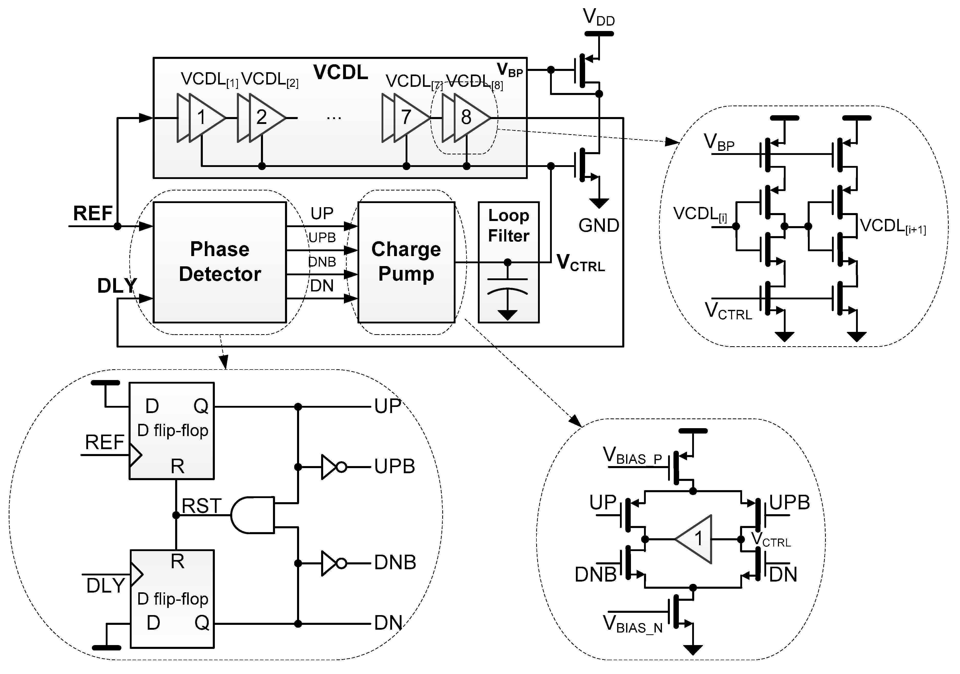
:1. Introduction
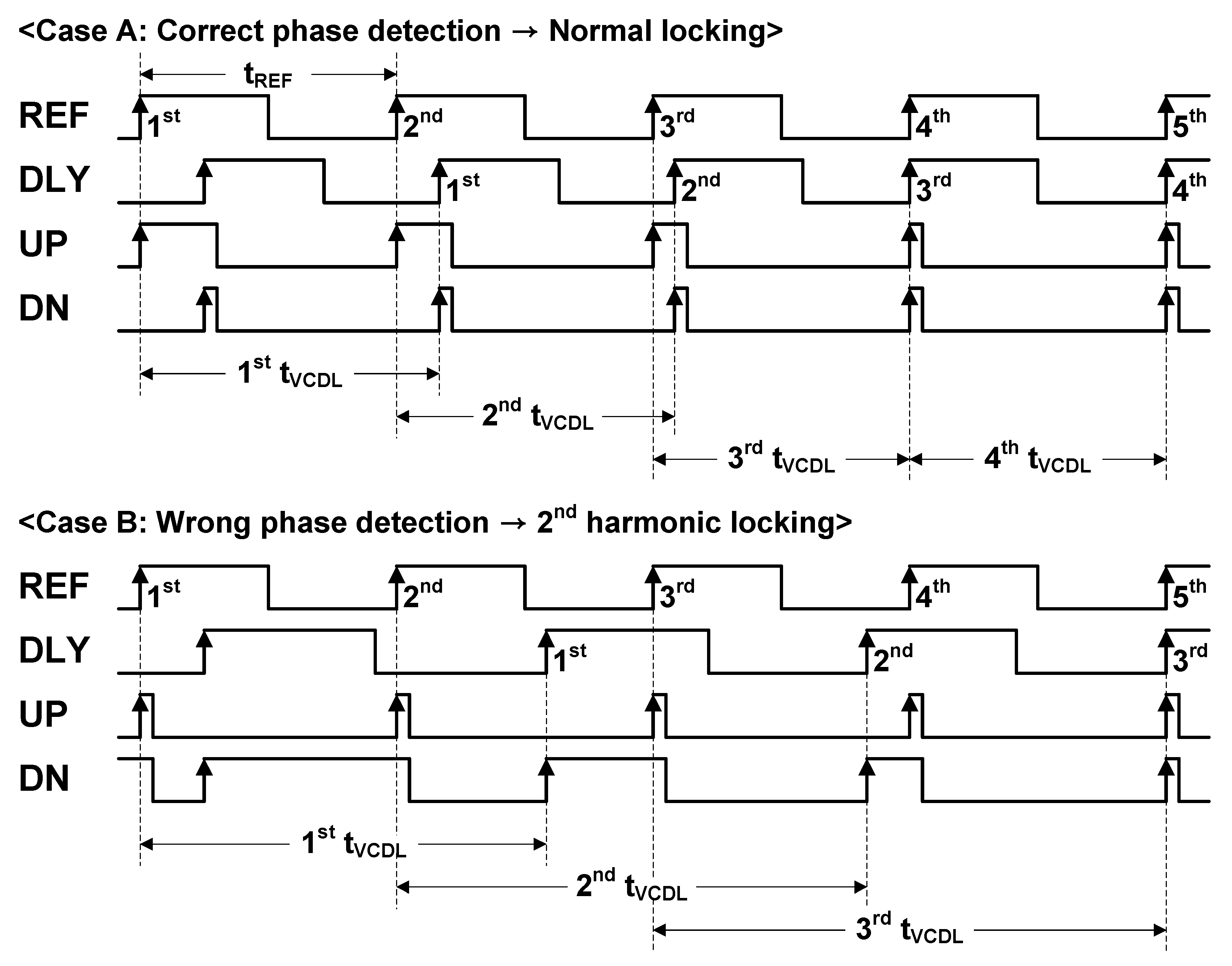
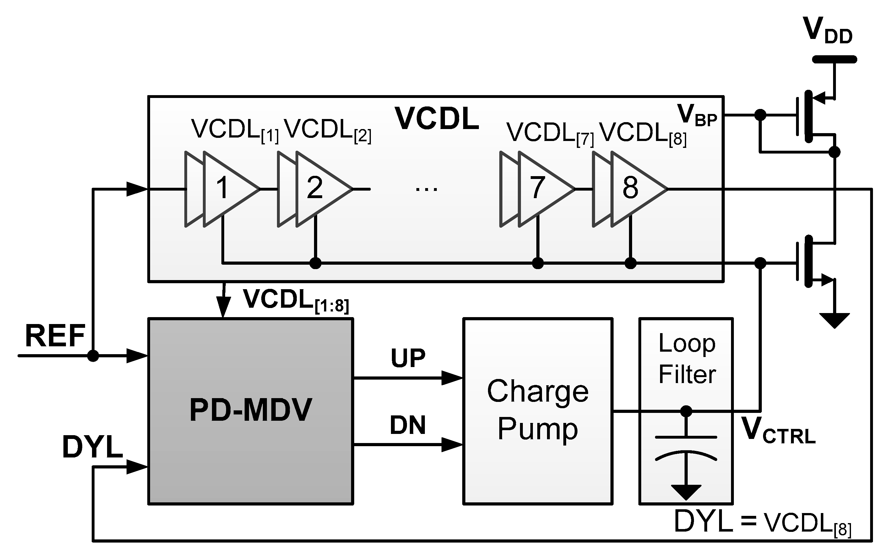
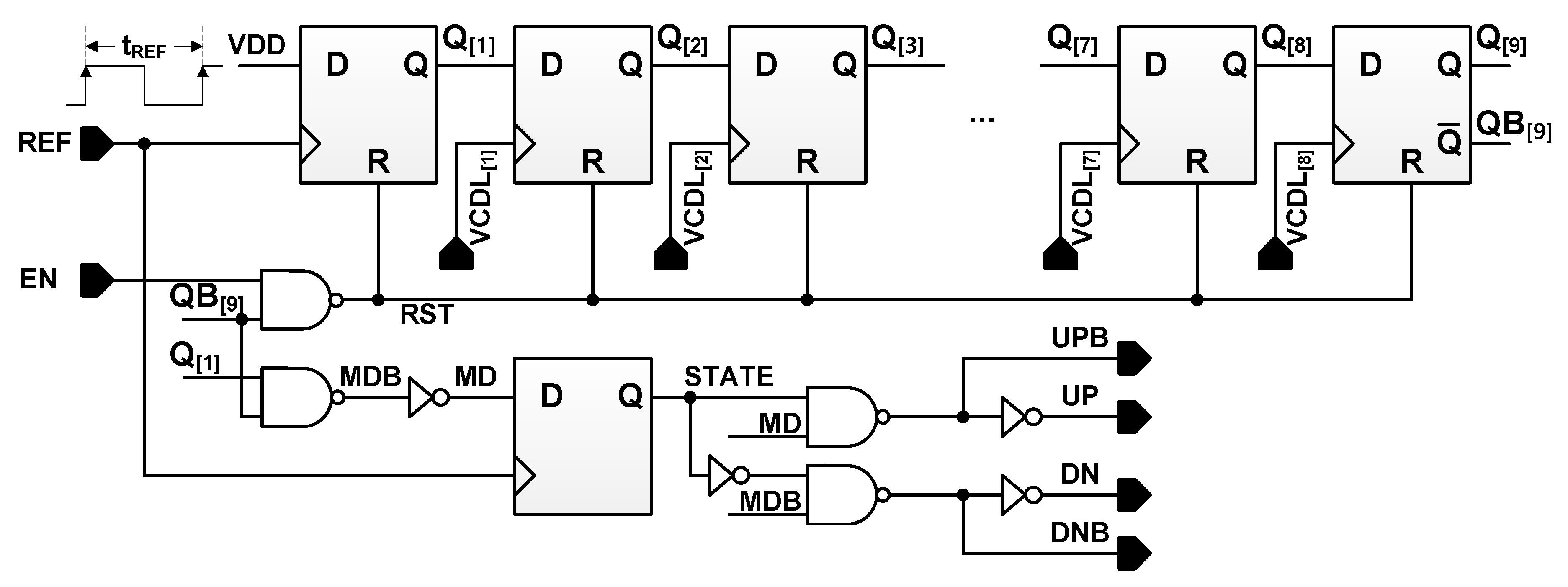
2. Proposed DLL with PD-MDV
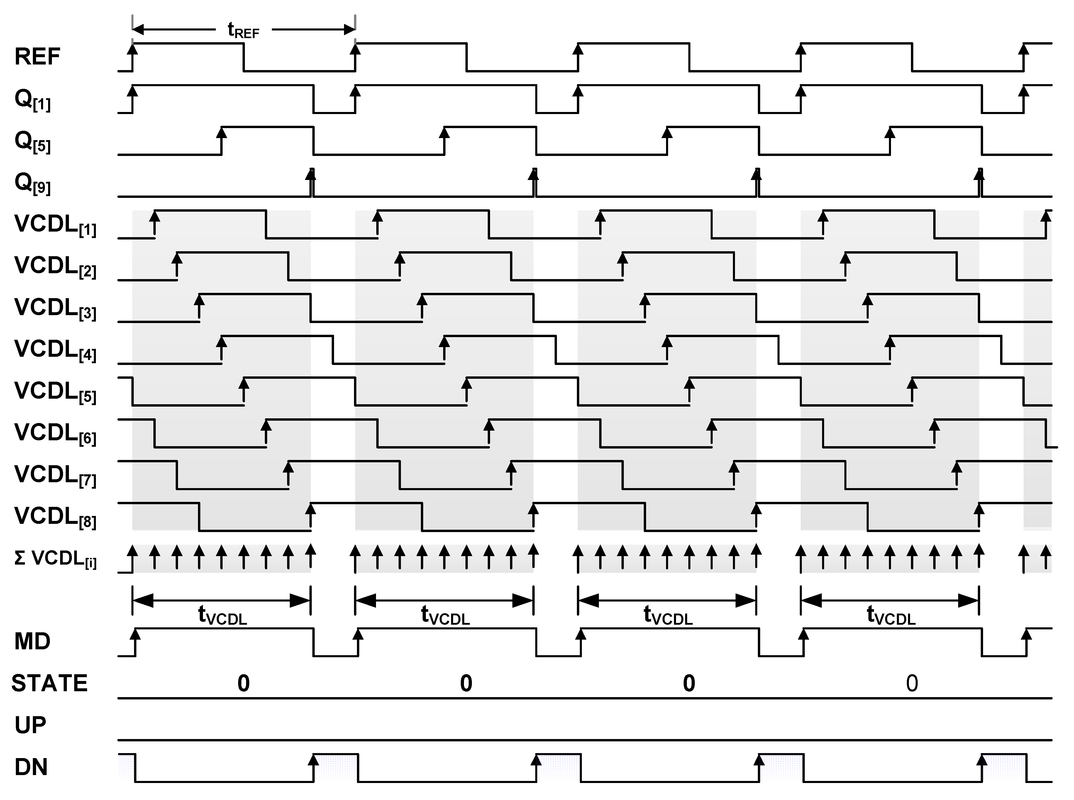
2.1. Case 1: PD-MDV Operation with Fixed High VCTRL for tVCDL < tREF
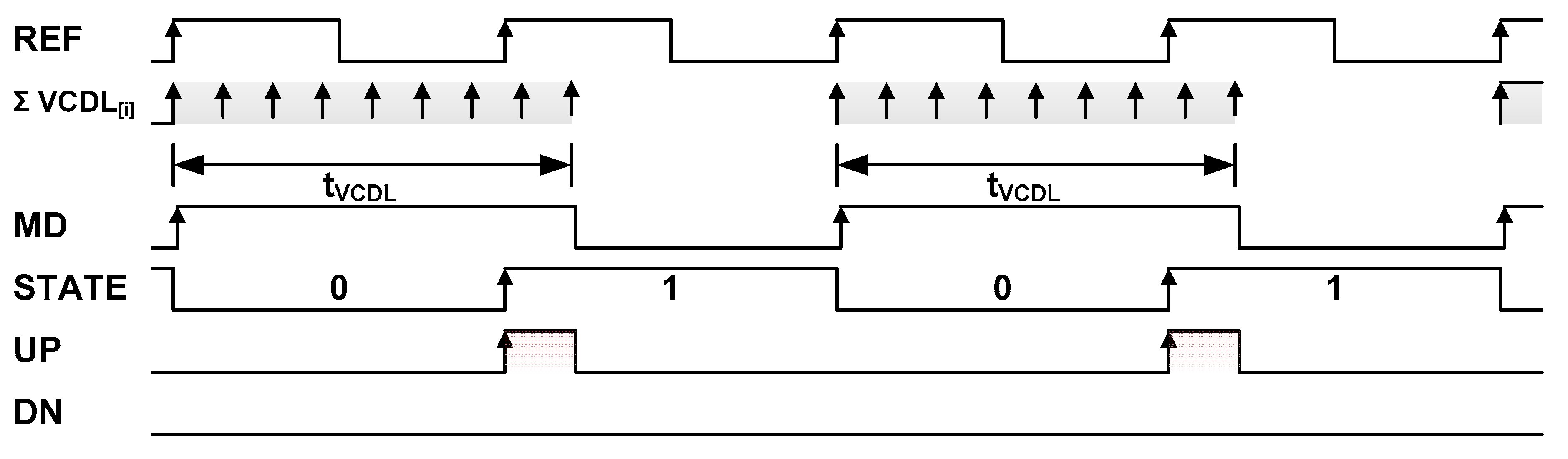
2.2. Case 2: PD-MDV Operation with Fixed Middle VCTRL for tREF < tVCDL ≤ 2·tREF
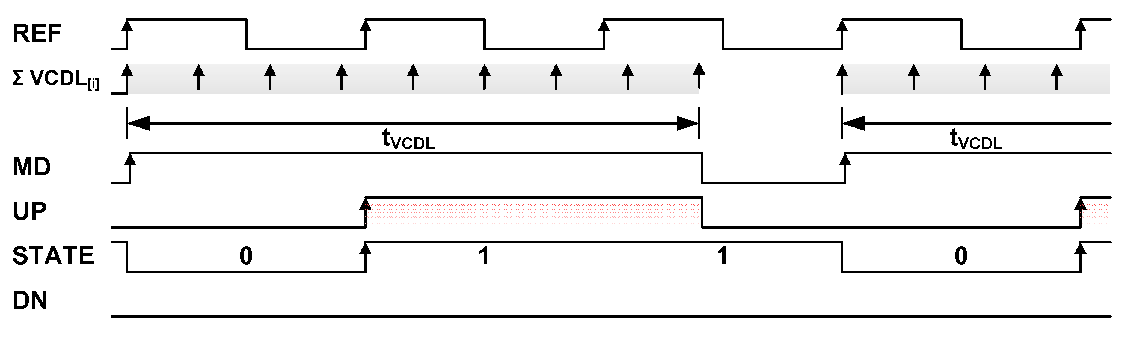
2.3. Case 3: PD-MDV Operation with Fixed Low VCTRL for tVCDL > 2·tREF
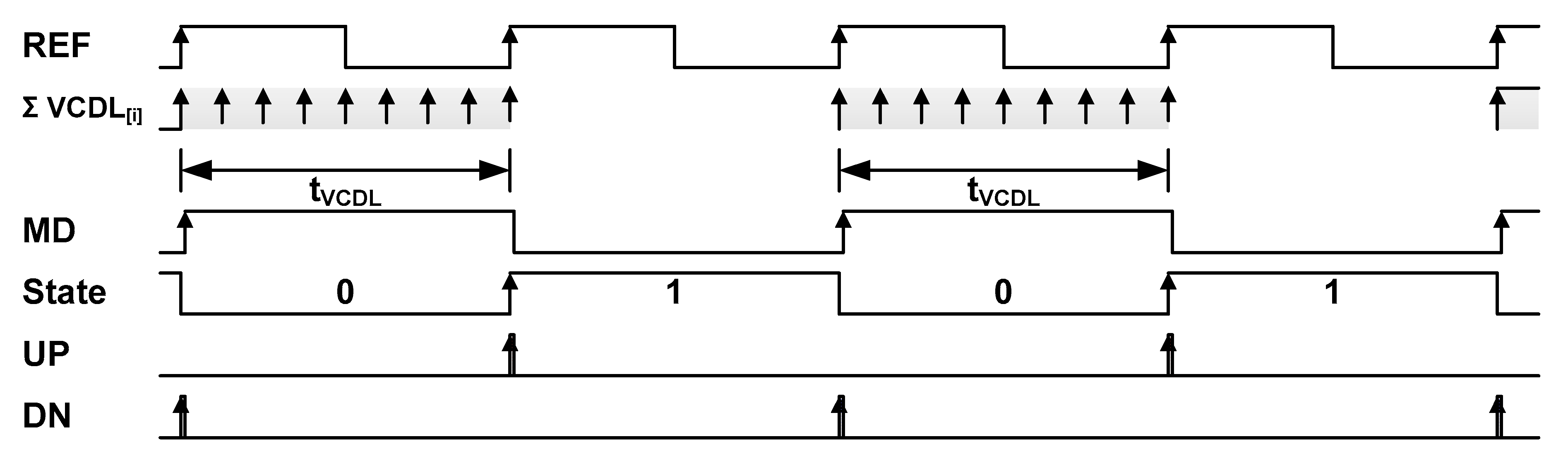
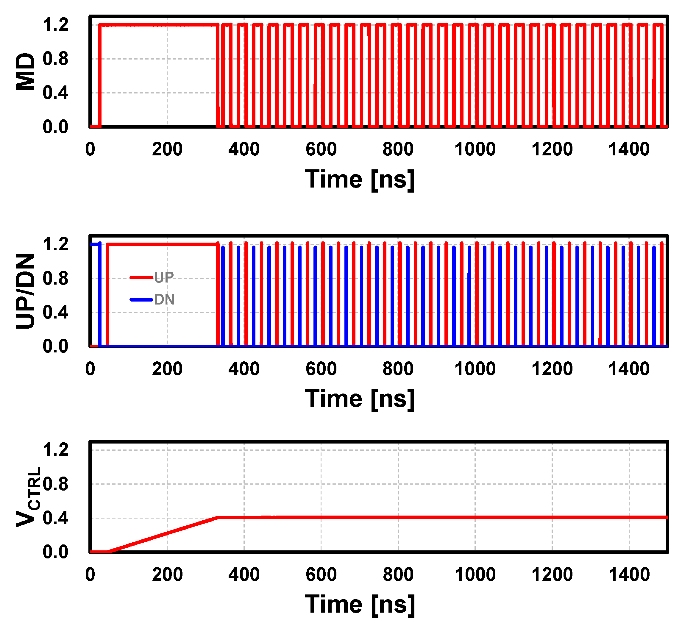
2.4. Understanding of STATE Signal
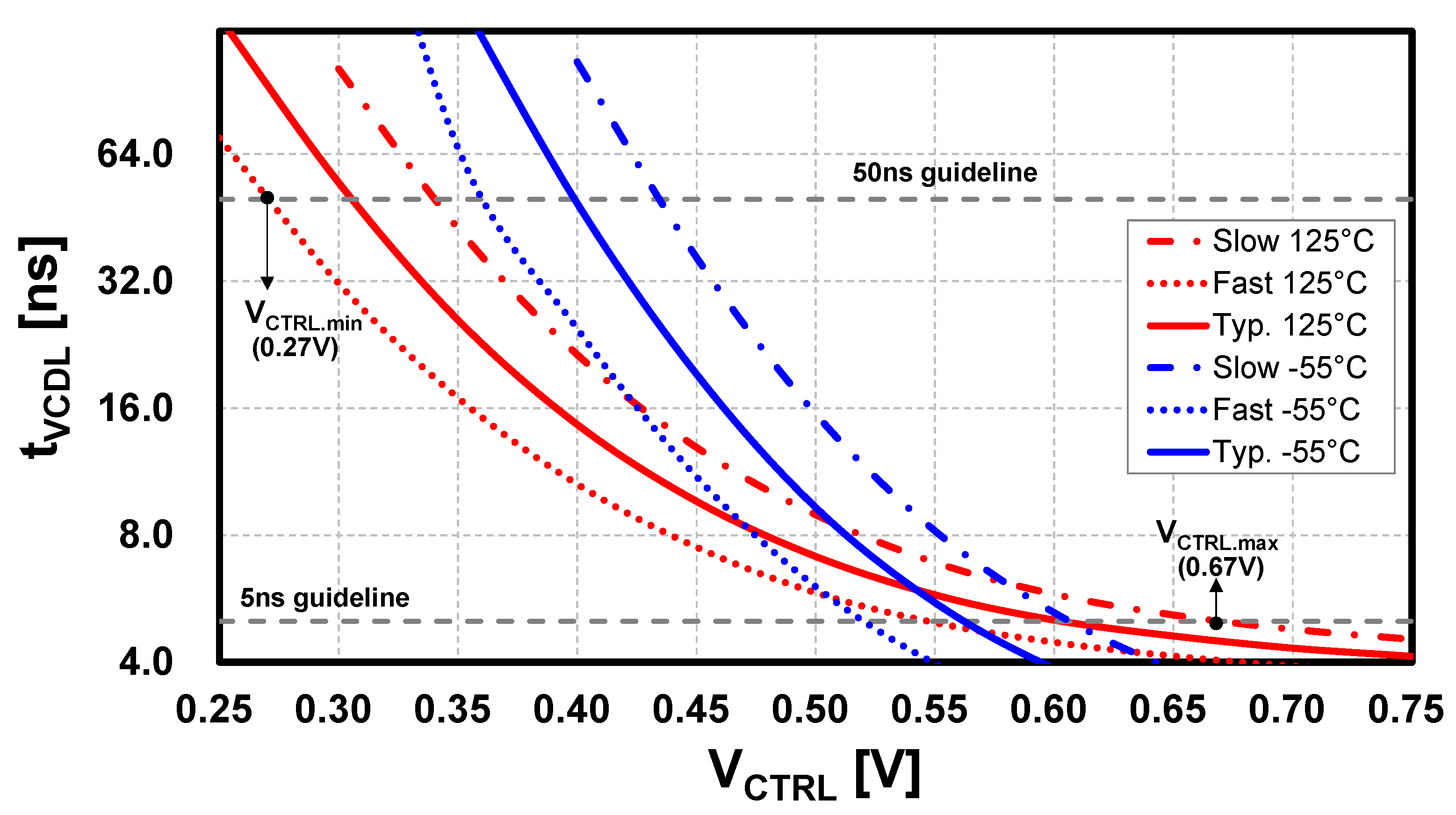
2.5. Design of Voltage-Controlled Delay Line
3. Performance Evaluations
4. Conclusions
Author Contributions
Funding
Institutional Review Board Statement
Informed Consent Statement
Data Availability Statement
Acknowledgments
Conflicts of Interest
References
- Spilker, J.; Magill, D. The Delay-Lock Discriminator-An Optimum Tracking Device. IEEE Proc. IRE 1961, 49, 1403–1416. [Google Scholar] [CrossRef]
- Moon, Y.-H.; Kong, I.-S.; Ryu, Y.-S.; Kang, J.-K. A 2.2-mW 20–135-MHz False-Lock-Free DLL for Display Interface in 0.15-μm CMOS. IEEE Trans. Circuits Syst. II Express Briefs 2014, 61, 554–558. [Google Scholar] [CrossRef]
- Rezaeian, A.; Ardeshir, G.; Gholami, M. Low-power and wide-band delay-locked loop with switching delay line. Int. J. Circuit Theory Appl. 2018, 46, 2189–2201. [Google Scholar] [CrossRef]
- Abbas, W.; Mehmood, Z.; Seo, M. A V-Band Phase-Locked Loop with a Novel Phase-Frequency Detector in 65 nm CMOS. Electronics 2020, 9, 1502. [Google Scholar] [CrossRef]
- Zhang, D.; Yang, H.-G.; Zhu, W.; Li, W.; Huang, Z.; Li, L.; Li, T. A Multiphase DLL With a Novel Fast-Locking Fine-Code Time-to-Digital Converter. IEEE Trans. Very Large Scale Integr. (VLSI) Syst. 2015, 23, 2680–2684. [Google Scholar] [CrossRef]
- Chung, C.-N.; Liu, S.-I. A 20-MHz to 3-GHz Wide-Range Multiphase Delay-Locked Loop. IEEE Trans. Circuits Syst. II Express Briefs 2009, 56, 850–854. [Google Scholar] [CrossRef]
- Ng, H.J.; Fischer, A.; Feger, R.; Stuhlberger, R.; Maurer, L.; Stelzer, A. A DLL-Supported, Low Phase Noise Fractional-N PLL With a Wideband VCO and a Highly Linear Frequency Ramp Generator for FMCW Radars. IEEE Trans. Circuits Syst. I Regul. Pap. 2013, 60, 3289–3302. [Google Scholar] [CrossRef]
- Jang, S.; Song, H.; Ye, S.; Jeong, D.-K. A 13.8mW 3.0Gb/s Clock-Embedded Video Interface with DLL-Based Data-Recovery Circuit. In Proceedings of the IEEE International Solid-State Circuits Conference (ISSCC), San Francisco, CA, USA, 20–24 February 2007; pp. 450–452. [Google Scholar]
- Kim, J.; Ko, Y.; Jin, J.; Choi, J.; Chun, J.-H. A Referenceless Digital CDR with a Half-Rate Jitter-Tolerant FD and a Multi-Bit Decimator. Electronics 2022, 11, 537. [Google Scholar] [CrossRef]
- Park, S.; Kim, J.; Hwang, C.; Park, H.; Yoo, S.; Seong, T.; Choi, J. A 0.1–1.5-GHz Wide Harmonic-Locking-Free Delay-Locked Loop Using an Exponential DAC. IEEE Microw. Wirel. Compon. Lett. 2019, 29, 548–550. [Google Scholar] [CrossRef]
- Chung, K.; Koo, J.; Kim, S.-W.; Kim, C. An Anti-Harmonic, Programmable DLL-Based Frequency Multiplier for Dynamic Frequency Scaling. In Proceedings of the 2007 IEEE Asian Solid-State Circuits Conference (ASSCC), Jeju, Korea, 12–14 November 2007; pp. 276–279. [Google Scholar]
- Cheng, K.-H.; Lo, Y.-L. A Fast-Lock Wide-Range Delay-Locked Loop Using Frequency-Range Selector for Multiphase Clock Generator. IEEE Trans. Circuits Syst. II Express Briefs 2007, 54, 561–565. [Google Scholar] [CrossRef]
- Song, E.; Lee, S.-W.; Lee, J.-W.; Park, J.; Chae, S.-I. A reset-free anti-harmonic delay-locked loop using a cycle period detector. IEEE J. Solid-State Circuits 2004, 39, 2055–2061. [Google Scholar] [CrossRef]
- Mohamed, A.K.; Ibrahim, S.A.; Abo-Elsoud, M.E.A. A 3.3-mW Low Phase Noise VCDL for Factorial Delay-Locked Loops. In Proceedings of the 36th National Radio Science Conference (NRSC), Port Said, Egypt, 16–18 April 2019; pp. 299–304. [Google Scholar]
- Jang, C.-S.; Choi, J.-C.; Park, J.-H.; Chung, I.-J.; Kwon, O.-K. An intra interface of flat panel displays for high-end TV appli-cations. IEEE Trans. Consum. Electron. 2008, 54, 1447–1452. [Google Scholar] [CrossRef]
- Sung, G.; Chou, W.; Chiu, T. Optical transceiver with deficit round robin and RS232 interface for synchronous optical net-working. In Proceedings of the IEEE International Conference on Systems, Man, and Cybernetics (SMC), Budapest, Hungary, 9–12 October 2016; pp. 003166–003170. [Google Scholar]
- Bae, W. State-of-the-Art Circuit Techniques for Low-Jitter Phase-Locked Loops: Advanced Performance Benchmark FOM Based on an Extensive Survey. In Proceedings of the IEEE International Symposium on Circuits and Systems (ISCAS), Daegu, Korea, 22–28 May 2021; pp. 1–5. [Google Scholar]
- Dai, S.; Rosenstein, J.K. A 14.4 nW 122 kHz Dual-phase Current-mode Relaxation Oscillator for Near-Zero-Power Sensors. In Proceedings of the IEEE Custom Integrated Circuits Conference (CICC), San Jose, CA, USA, 28–30 September 2015; pp. 1–4. [Google Scholar]
- Tong, J.; Wang, S.; Zhang, S.; Zhang, M.; Zhao, Y.; Zhao, F. A Low-Jitter Harmonic-Free All-Digital Delay-Locked Loop for Multi-Channel Vernier TDC. Sensors 2022, 22, 284. [Google Scholar] [CrossRef] [PubMed]
- Modanlou, S.; Ardeshir, G.; Gholami, M. Analysis and design of a low jitter delay-locked loop using lock state detector. Int. J. Circuit Theory Appl. 2021, 49, 1410–1419. [Google Scholar] [CrossRef]


| Case 1 | Case 2 | Case 3 | |
|---|---|---|---|
| STATE = ‘0’ | DN = MDB UP = ‘0’ | Same as the left | Same as the left |
| STATE = ‘1’ | Nor occurred (Don’t care) | DN = ‘0’ UP = MD | Same as the left |
| [2] | [5] | [12] | [19] | [20] | This Work * | |
|---|---|---|---|---|---|---|
| Process (nm) | 150 | 130 | 250 | 55 | 180 | 65 |
| Supply (V) | 1.8 | 1.5 | 1.2 | 1.2 | 1.2 | 1.2 |
| Freq. range (MHz) | 20−135 | 80−450 | 32−320 | 560−800 | 125−875 | 20−200 |
| Power Consumption (mW) | 2.2 @130 MHz | 26 @180 MHz | 15 @320 MHz | 6.92 @800 MHz | 2.78 @250 MHz | 0.4 @200 MHz |
| Efficiency FoM (μW/MHz) | 16.9 | 125.6 | 46.9 | 8.7 | 11.1 | 2.0 |
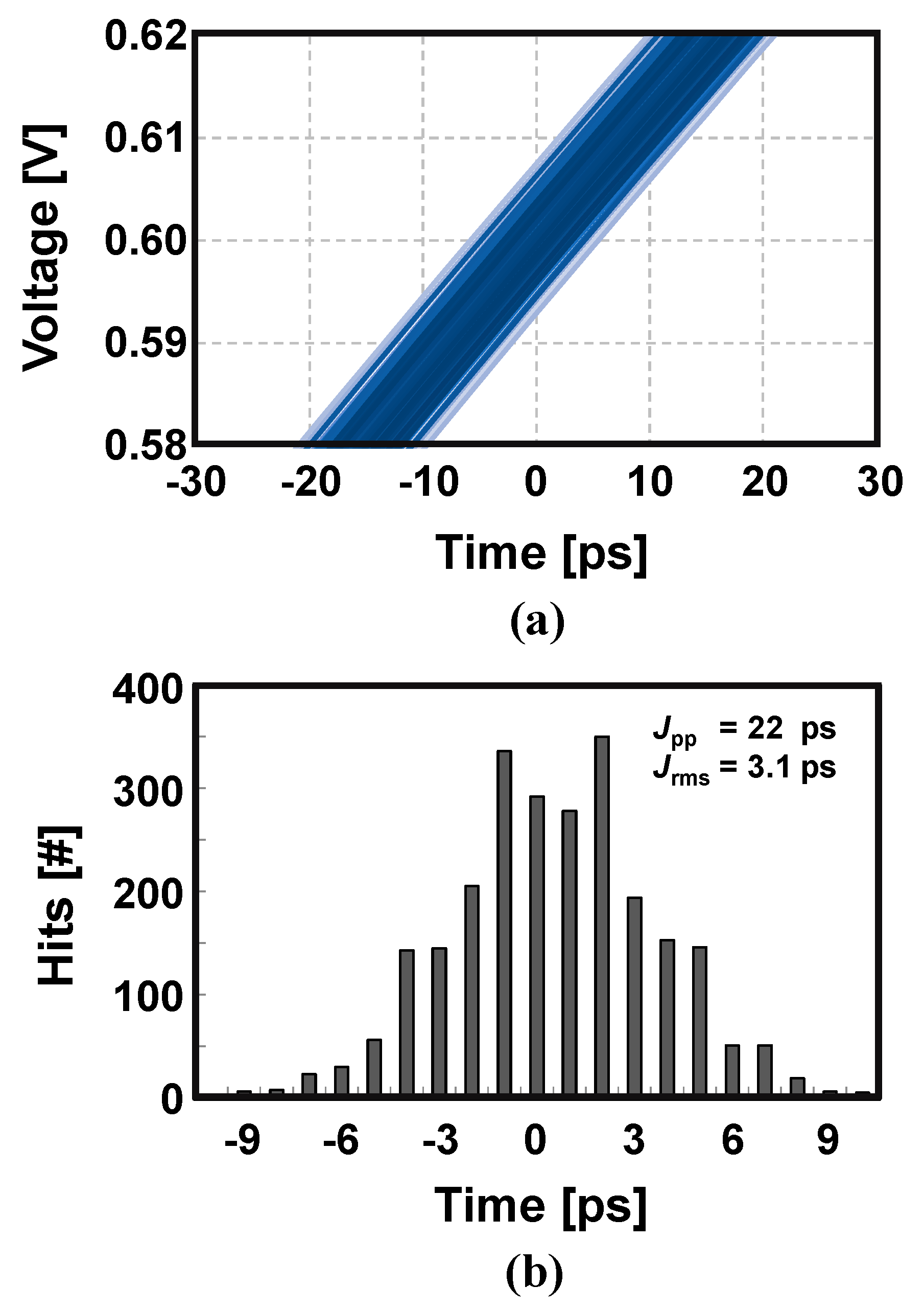
| Jitter RMS/Peak-to-Peak (ps) @fOUT | −/192 @100 MHz | 2.3/10 @180 MHz | 4.4/15 @200 MHz | 1.2/6.5 @800 MHz | 2.1/4.4 @250 MHz | 3.1/22 @200 MHz |
Publisher’s Note: MDPI stays neutral with regard to jurisdictional claims in published maps and institutional affiliations. |
© 2022 by the authors. Licensee MDPI, Basel, Switzerland. This article is an open access article distributed under the terms and conditions of the Creative Commons Attribution (CC BY) license (https://creativecommons.org/licenses/by/4.0/).
Share and Cite
Cho, S.-H.; Cho, Y.-K. A 1.2 V 0.4 mW 20~200 MHz DLL Based on Phase Detector Measuring the Delay of VCDL. Electronics 2022, 11, 2434. https://doi.org/10.3390/electronics11152434
Cho S-H, Cho Y-K. A 1.2 V 0.4 mW 20~200 MHz DLL Based on Phase Detector Measuring the Delay of VCDL. Electronics. 2022; 11(15):2434. https://doi.org/10.3390/electronics11152434
Chicago/Turabian StyleCho, Sang-Hyun, and Young-Kyun Cho. 2022. "A 1.2 V 0.4 mW 20~200 MHz DLL Based on Phase Detector Measuring the Delay of VCDL" Electronics 11, no. 15: 2434. https://doi.org/10.3390/electronics11152434
APA StyleCho, S.-H., & Cho, Y.-K. (2022). A 1.2 V 0.4 mW 20~200 MHz DLL Based on Phase Detector Measuring the Delay of VCDL. Electronics, 11(15), 2434. https://doi.org/10.3390/electronics11152434