Abstract
To overcome the weakness of the narrow conversion gain of dual bridge resonant converter, a half-dual bridge resonant converter (H-DBRC) with voltage match modulation (VMM) is proposed and implemented for wide voltage range applications. The H-DBRC, including a full bridge on the primary side and a half bridge on the secondary side, is adopted to realize the bidirectional power flow and wide voltage operation. Owing to the synergy between the H-DBRC structure and VMM strategy, the converter can operate in full-bridge state and half-bridge state with maximized ZVS (zero-voltage switching) operation and minimized circulating current. The steady-state analysis is performed and the solutions for both forward and backward modes could be obtained uniformly by using the fundamental harmonics approximation approach. The soft-switching characteristics, implementation process and design example are analyzed in detail. Finally, to confirm the theoretical analysis and feasibility, both simulation and experimental verifications are demonstrated in this paper. Since the converter consistently achieves voltage-matching operation, the optimal ZVS range can be obtained when the voltage gain M is between 0.5 to 1. Moreover, the economic cost and control complexity are greatly reduced because only six switches are required in the converter.
1. Introduction
Due to the features of electrical isolation, bidirectional energy flow, high power density and ability to achieve soft-switching, the dual active bridge DC-DC converters (DAB) and dual bridge resonant converters (DBRC) are widely used in a series of applications such as electric vehicles (EVs) [1,2], smart grids [3], energy storage systems (ESS) [4], and renewable energy systems. To meet the requirements of battery applications, converters should operate with bidirectional power transfer and soft-switching in a wide voltage range [5]. The conventional modulation strategy of a DAB or DBRC is the single phase shift (SPS) modulation [6,7]. The power flow direction and amplitude can be regulated just by controlling the phase shift between the primary side bridge and the secondary side bridge. When voltage gain is equal to 1, the converter has good performance, such as the lowest current stress and widest zero-voltage switching (ZVS) range. However, when voltage gain is far from 1, ZVS operation is hard to realize and circulating current increase dramatically [8].
To improve the converter performance under wide voltage variation conditions, plenty modulation strategies extended from SPS are proposed [9]. By adding inner phase shift in the primary side bridge or secondary side bridge of DAB or DBRC, SPS is changed to extended phase shift (EPS) [10,11], dual phase shift (DPS) [12,13], and triple phase shift (TPS) [14,15] modulation. At the same time, the analysis and implementation of the converter with these modulations becomes complex due to the existence of more control variables [16,17,18]. In [19,20], an asymmetric pulse width modulation (APWM) is proposed for DBRC and a control route with minimized rms tank current is developed to decrease the conduction power loss. Similarly, an extended pulse width modulation (EPWM) with three control variables is proposed to extend ZVS range at light load [21]. The main problem of the two modulations is that ZVS operation for all eight switches can not be realized. A hybrid modulation is proposed in [22], when the normalized voltage gain is 0.5 or 1, the performance of DAB can be enhanced. However, when voltage gain is between 0.5 and 1, the modulation strategy is invalid.
In addition to optimizing the modulation strategies, large numbers of converters with variant topologies are proposed to enhance performance under wide voltage variation conditions [23,24,25]. An asymmetrical dual bridge converter based on dual transformers with secondary-side phase-shift control strategy is proposed in [26]. A hybrid-bridge DAB using voltage match control is proposed in [27], which has an auxiliary half-bridge structure on the primary side. In addition, a hybrid-bridge DBRC used in photovoltaic solar panel applications of bidirectional power flow and wide voltage range is proposed in [28]. The main drawback of these converters is that the additional switches and components will result in cost increase and control complexity. A simpler hybrid-bridge converter with six switches is proposed in [29], when voltage gain varies from 0.5 to 1, the performance of the converter can be improved. However, due to the non-resonant topologies, a dc blocking capacitor is needed to absorb the voltage offset. In [30], a dual-transformer based inductor-inductor-capacitor (LLC) resonant converter is proposed, the soft-switching range is extend over a wide input voltage and load level. However, the structure of two transformers will cause low power density and design difficulty. In order to realize wider operation range of input/output voltage, LLC resonant converters with serial and parallel topologies are analyzed in [31,32]. The main problem of these converters is that they can not realize bidirectional power flow.
To achieve wide voltage gain operation for bidirectional power flow applications, a half-dual bridge resonant converter (H-DBRC) with voltage match modulation (VMM) is presented in this paper. It is called half-DBRC because the topology is composed of a full bridge in the primary side and a half bridge in the secondary side. In addition, the two bridges are connected with a high-frequency transformer and a LC resonant tank. Moreover, VMM is employed to realize optimal performance with maximized ZVS operation and minimized circulating current in a wide range of voltage variation. The main idea of VMM is to keep the equivalent voltage gain equal to 1, more specifically, the equivalent amplitude of the primary ac voltage and secondary ac voltage are forced to be equal. Therefore, the primary-side ac voltage is modulated to an unbalanced waveform, to guarantee the voltage match with secondary-side ac voltage. The waveform has unbalanced characteristic because the negative pulse width is always equal to while the positive pulse width is an adjustable value. The dc bias voltage is naturally balanced due to the existence of resonant capacitor. And the output power is still regulated by phase shift between primary side bridge and secondary side bridge. Since voltage match is realized for H-DBRC with VMM over the entire voltage range, a wide ZVS range can be achieved and the circulating current is naturally reduced.
Owing to the synergy between the H-DBRC structure and VMM strategy, high performance of the converter in a wide voltage range can be achieved. The merits and contributions of this paper are as follows:
(1) The structure of H-DBRC requires only six switches, that means the economic cost and control complexity can be greatly reduced. And wide-voltage-range operation can be realized in a cost-efficient way.
(2) Since the converter consistently achieves voltage matching with VMM strategy when the voltage gain M is between 0.5 and 1, ZVS of all the switches is achieved in a wide range.
(3) The optimal ZVS range and minimum circulating current can be obtained in both full-bridge and half-bridge states when and .
(4) The proposed converter can realize bidirectional power transmission with similar characteristics under a unified model.
This paper is organized as follows. Section 2 describes the topology of proposed H-DBRC and the operation principle of two modes. Section 3 presents the steady-state snalysis of H-DBRC with VMM and soft-switching conditions. Then in Section 4, a design example is given, simulation and experimental results are included to verify the theoretical analysis. Section 5 concludes the paper.
2. Topology and Operation Principle of H-DBRC
The topology of the H-DBRC is shown in Figure 1. The converter consists of a full bridge, a half bridge, a series resonant tank with a inductor () and a capacitor (), and a high-frequency (HF) transformer (). ∼ are six switches, ∼ and ∼ are the body diodes and parasitic capacitors respectively, and are output capacitors. and are the ac voltages on the primary side and secondary side, respectively. is input voltage and is output voltage. The leakage inductance of the HF transformer can be regarded as part of the resonant inductor (). In addition, the resonant capacitor is connected in series with the transformer, which can act as a DC blocking capacitor to prevent saturation of the HF transformer. The primary-side full bridge can be configured as a half bridge, when is always on and is always off. Beyond that, the converter allows power to flow forward and backward, which results in bidirectional energy transfer.
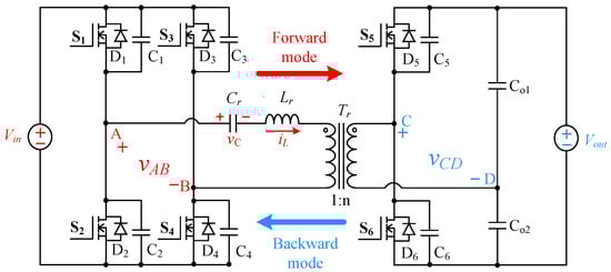
Figure 1.
Topology of the proposed Half-Dual Bridge Resonant Converter.
2.1. Forward Mode
The steady-state waveforms of H-DBRC in forward mode are shown in Figure 2. With VMM strategy, and are operated with duty cycle. The on-time duration of in one HF period is decreased to while the on-time duration of is increased to 2, the range of is . Therefore, an unbalanced three-level waveform voltage with adjustable pulse-width is generated. It has a positive pulse-width , a zero-voltage portion , and the negative pulse width is always equal to . Switches and are also operated with duty cycle, therefore, is constantly a square-wave voltage signal. In addition, there is a phase-shift angle between the two bridges that directs the power flow from one side to the other. It is defined as the angle by which the gating signal of leads that of . It can be seen from Figure 2 that there are 7 different intervals in one switching cycle. Figure 3 shows equivalent circuits during various intervals.
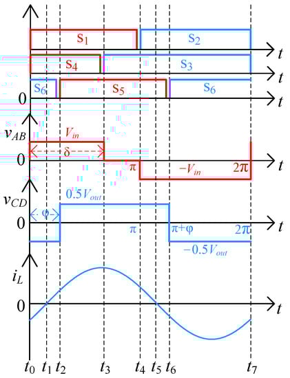
Figure 2.
The steady-state waveforms of H-DBRC in forward mode.
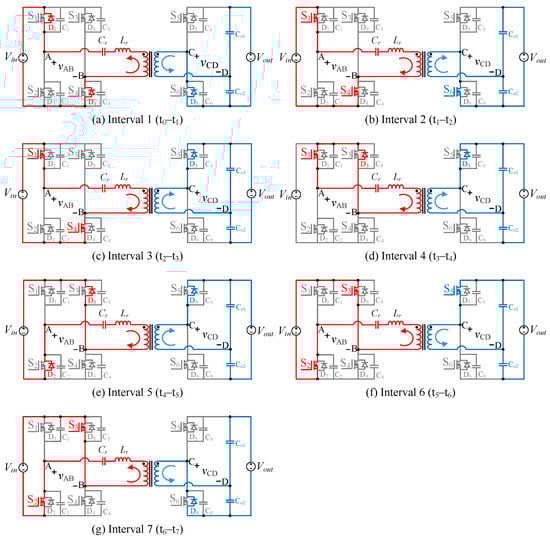
Figure 3.
Equivalent circuits during different time intervals in forward mode.
(1) Interval 1 (–)
As shown in Figure 2, at , and are turned off, and are turned on. Due to the resonant current is negative, the current flows through , , and the ac voltage of the primary side . The current flows through and , on the secondary side. Therefore, the ac voltage . The equivalent circuit for interval 1 is depicted in Figure 3a.
(2) Interval 2 (–)
The resonant current increases to 0 at time . In this interval, the resonant current is positive. The resonant current flows through switches , on the primary side, and the voltage . The current flows through and , on the secondary side. Therefore, the ac voltage . This interval ends when is turned off. The equivalent circuit for interval 2 is depicted in Figure 3b.
(3) Interval 3 (–)
At , switches is turned off, and is turned on. The resonant current still keeps increasing. The primary-side full bridge has the same state as interval 2 and the voltage . The current flows through the and , on the secondary side. Therefore, the ac voltage . The equivalent circuit for interval 3 is depicted in Figure 3c.
(4) Interval 4 (–)
As shown in Figure 2, at , is turned off, and is turned on. On the primary side, is equal to 0 since it is shorted by and . The current gradually decreases in this interval. The secondary-side bridge has the same state as interval 3 and the voltage . The equivalent circuit for interval 4 is depicted in Figure 3d.
(5) Interval 5 (–)
When , turned off, and turned on. The resonant current still keeps dropping until it reaches 0 in this interval. On the primary side, the current flows through , , and the voltage . On the secondary side, the current flows through the and , , the voltage . The equivalent circuit for interval 5 is depicted in Figure 3e.
(6) Interval 6 (–)
In this interval, the polarity of the resonant current changes and it begins to increase in reverse. So, the current is negative. On the primary side, the current flows through , , and the voltage . On the secondary side, the current flows through the , the voltage . The conducting devices and current path are shown in shown in Figure 3f.
(7) Interval 7 (–)
After switch is turned off and is turned on, the voltage of changes from to . As shown in Figure 3g, on the primary side, the resonant current flows through , . The current flows through the , on the secondary side.
2.2. Backward Mode
The steady-state waveforms of H-DBRC in backward mode are shown in Figure 4. The converter is still controlled with VMM strategy. The primary-side switches are operated in the same state of forward mode, and the secondary-side switches and are still operated at duty cycle. The difference is the gating signal of leads that of in a certain angle in backward mode. Since there is no change of the definition of angle , the phase shift between and is . There are also 7 different intervals during one switching cycle in this mode. Figure 5 shows the equivalent circuit during the different time intervals.
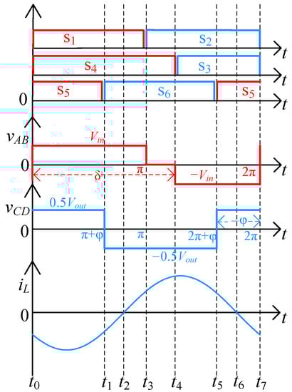
Figure 4.
The steady-state waveforms of H-DBRC in backward mode.
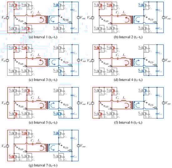
Figure 5.
Equivalent circuits during different time intervals in backward mode.
(1) Interval 1 (–)
As shown in Figure 4. This interval begins when , are turned off and , are turned on at . Since the resonant current is negative, the current flows through , on the primary side, and the voltage . On the secondary side, the current flows through the switch , the voltage . The equivalent circuit for interval 1 is depicted in Figure 5a.
(2) Interval 2 (–)
When , turned off and turned on. On the primary side, the resonant current flows through , , and the voltage . The current gradually increases in this interval. On the secondary side, the current flows through the switch and , , the voltage . This interval ends when is turned off. The equivalent circuit for interval 2 is depicted in Figure 5b.
(3) Interval 3 (–)
In this interval, the resonant current increases to 0 from to . After switch is turned off and switch is turned on, is equal to . As shown in Figure 5c, The primary-side full bridge has the same state as interval 2 and the voltage . The current flows through and , on the secondary side.
(4) Interval 4 (–)
This interval begins when the resonant current reaches 0 at . Although the voltage is still equal to 0, the resonant current flows through , on the primary side. On the secondary side, the current flows through the switch , the voltage . The equivalent circuit for interval 4 is depicted in Figure 5d.
(5) Interval 5 (–)
At , turned off and turned on, the resonant current is positive in this interval. The primary current flows through anti-parallel diodes and , the voltage . On the secondary side, the current flows through the switch and , , the voltage . The conducting devices and current path for interval 5 are depicted in Figure 5e.
(6) Interval 6 (–)
When , is turned off and is turned on. The resonant current keeps dropping until it reaches 0 in this interval. The primary-side full bridge has the same state as interval 4 and the voltage . On the secondary side, the current flows through the , the voltage . The equivalent circuit for interval 6 is depicted in Figure 5f.
(7) Interval 7 (–)
The polarity of the resonant current changes and the current is negative in this interval. On the primary side, the current flows through , , the voltage . On the secondary side, the current flows through the switch , the voltage . The equivalent circuit for interval 7 is depicted in Figure 5g.
3. Steady-State Analysis of H-DBRC with VMM
To facilitate the calculation and design, all equations presented are normalized with the base values given later. All parameters in the secondary side have been transferred to the primary side, which is denoted by the superscript “ ”.
where is rate power, is the equivalent output load, is the turns ratio of the transformer. The normalized switching frequency is given by:
where is the resonant frequency and is the switching frequency. Then normalized impedance of the resonant tank are given by:
where Q is the quality factor and is defined as follows:
The Fundamental Harmonics Approximation (FHA) approach can simplify the calculation for the steady-state analysis. The equivalent circuit of the converter in the phasor domain is depicted in Figure 6, and the two fundamental voltage phasors are shown as follows:
where M is the voltage gain of the converter and is defined as:
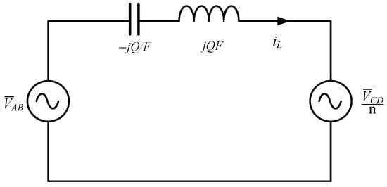
Figure 6.
The equivalent circuit in the phasor domain.
According to the equivalent circuit shown in Figure 6, the normalized inductor current expression can be written as:
where the peak current and the phase angle are:
Then, the normalized power expression can be derived as:
Since the definition of between forward mode and backward mode is the same, the expression of output power can be unified. And the boundary condition of the two modes can be obtained:
When , the converter operates in forward mode. When , the converter operates in backward mode. Figure 7a,b show the 3-dimensional plots of the normalized power with the control of and in forward and backward modes, respectively, in which the red curves are their boundary.
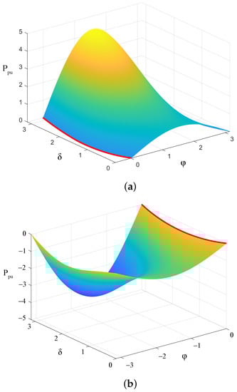
Figure 7.
3-dimensional plots of normalized power: (a) Fordward mode, (b) Backward mode.
3.1. Implementation of the Proposed VMM Strategy
VMM is employed to realize optimal performance with maximized ZVS operation and minimized circulating current in a wide range of voltage variation. The main idea of VMM is to keep the equivalent voltage gain equal to 1, more specifically, the equivalent amplitude of the primary-side ac voltage and secondary-side ac voltage are forced to be equal. Therefore, the following equation can be obtained:
Further, the equation can be simplified and voltage gain M can be expressed as:
When a fixed voltage gain M is given, the angle can be calculated. Then, the optimum operation condition can be obtained. Since the range of is [0, ], the proposed H-DBRC with VMM realizes a general voltage match when .
By combining Equations (10) and (13), another control variable can be easily calculated at a given voltage gain M and power ratio K:
where is the power ratio.
The diagram of the implementation of the proposed VMM strategy is presented in Figure 8. Firstly, the input voltage and output voltage are measured by voltage sensors. Then the PI output and voltage gain M are calculated. After that, the control variables and can be calculated by VMM strategy. Finally, the gating singles are generated by a PWM unit according to the control variables. The entire control loop is straightforward and does not need any complex calculation since the analytical solution of the control variables can be expressed with VMM strategy.
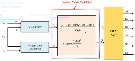
Figure 8.
Implementation of the proposed VMM strategy.
For further explanation of VMM strategy, the converter operation at different voltage gains are illustrated in detail. Taking forward mode as an example, the typical waveforms are shown in Figure 9. For the case of and , the obtained ac voltage and are both square waves, the converter operates at the optimal operating point with voltage match. Like SPS, only the outer phase shift angle between the primary-side and the secondary-side bridges is used to modulate the power transfer. When , as Figure 9a shows, the converter operates in half-bridge state, in which is always on and is always off. The ac voltage is a two-level wave of and 0. The dc bias voltage of is naturally balanced by the resonant capacitor and ZVS operation is realized over the entire load range. When , as shown in Figure 9c, the converter works in full-bridge state. is a two-level wave and the voltage amplitude is . In addition, ZVS can be ensured for whole load rang. As shown in Figure 9b, when , the converter works in the intermediate state, and the value of is between 0 and . Therefore, becomes an unbalanced three-level waveform of and 0. The dc bias voltage can also be balanced by the resonant capacitor.
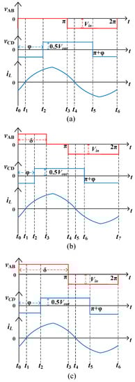
Figure 9.
Typical waveforms at different voltage gains: (a) ; (b) ; (c) .
3.2. Soft Switching Analysis
When the current flows through anti-parallelled diodes of MOSFETs, it ensures that the switches can realize ZVS operation. So, the basic principle to achieve ZVS is that the current direction needs to be against the voltage direction when the switch is turned on. Therefore, the ZVS conditions of ∼ in H-DBRC with VMM are shown in Table 1.

Table 1.
ZVS conditions.
From another perspective, the ZVS conditions can be illustrated graphically. Figure 10 shows the ZVS region with regard to the two control variables at different voltage gains. In each subfigure, the ZVS boundaries of different switches are shown for a particular voltage gain M, and the full ZVS region are shaded. The blue dashed line is an equal-power line, and the red point on the line indicates the working point with VMM strategy under the particular power level.
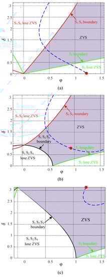
Figure 10.
ZVS Region with different voltage gains: (a) , (b) , (c) .
Figure 10a shows the ZVS region at . The equal-power line and working point can be obtained according to Equations (10) and (14). Since the control variable is always equal to 0, the converter is operating in the half-bridge state with VMM strategy, which means is always on and is always off. Although the working point is not in the full ZVS region, the switching loss can be neglected due to is not operating at high frequency. From this point of view, the best ZVS performance can be obtained when . Figure 10b shows the ZVS region when . Since it is an intermediate state, ZVS region is constrained by the converter working state, which is depend on the output power and voltage gain. In general, ZVS of all switches is easy to achieve in high power level due to a large . When , as shown in Figure 10c, the converter is operating in the full-bridge state and is always equal to . It can be seen that the full ZVS operation is achieved. Although VMM strategy is similar to conventional SPS modulation when , full ZVS operation is lost in SPS when M deviates from 1. Therefore, when the proposed VMM strategy is compared with SPS, it has an extended ZVS range. Furthermore, it is worth noting that, when voltage match is satisfied, a low circulating current is achieved. As all knows, the circulating current will increase the RMS value of resonant current and is no use for the output power. Therefore, the conduction loss and magnetic loss can be decreased by VMM strategy.
4. Simulation and Experimental Verification
4.1. Design Example
To validate the theoretical analysis of the converter with VMM strategy, H-DBRC was subjected to a number of experiments in the laboratory and computer simulations. Firstly, the specifications of the converter are determined as follows: is 75 V to 150 V, is 100 V, the switching frequency is 100 kHz and the rated power is 200 W. To achieve better performance, the design point is chosen at the maximum voltage gain , i.e., the minimum input voltage V. The converter is tested with three different values of voltage gain: the maximum gain at 1 ( V, V), the minimum gain at 0.5 ( V, V), and ( V, V).
Moreover, to have a certain soft-switching margin for the above resonant operation, the normalized frequency F is chosen to be 1.35. Therefore, according to Equation (6) the transformer turns ratio can be derived:
The base impedance is:
It is selected to adopt a full-load quality factor Q of 1. The resonant inductor and capacitance parameters can be calculated as follows:
4.2. Simulation Results
Before the experimental validation of the prototype, simulations were performed using PSIM software. Table 2 displays the specifications of the components in PSIM software. The steady-state operating waveforms of the forward mode using the proposed VMM strategy with different voltage gain M at rate power W as Figure 11 illustrated. Energy is transferred from to in the forward mode. The steady-state waveform at , with V and V, is depicted in Figure 11a–c. The plots in Figure 11a are, from top to bottom, as follows: output voltage , and , resonant current . Figure 11b are the current of and the plots shown in Figure 11c are the current of . It can be seen that both and are square waves with duty cycle, the resonant current is approximately sinusoidal. Since the converter is operating in half-bridge state, switch is always closed and is always turned on. The optimal performance with full ZVS operation and low circulating current is realized. Figure 11d–f shows the steady-state waveforms at . It can be seen that is a three-level waveform with a maximum value of 125 V, while is still a square waveform with an amplitude of 50 V and a duty cycle of . The resonant current is approximately sinusoidal and ZVS is achieved for all six switches. Figure 11g–i shows the steady-state waveforms at , it can be seen that and are square waves with no dc bias, where has an amplitude of 75 V and has an amplitude of 50 V. The optimal performance is achieved with full ZVS operation and low circulating current due to voltage match.
Table 2.
The specifications of the components in simulation.
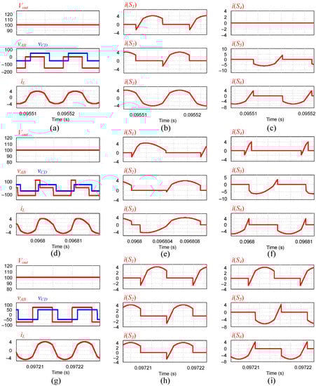
Figure 11.
Simulation results of forward mode with different voltage gain M: (a–c) ; (d–f) ; (g–i) .
In order to validate the feature of bidirectional power flow, the backward mode with different voltage gain M is also tested. Figure 12 shows the steady-state operating waveforms at rate power W. Figure 12a–c shows the steady-state waveforms at and Figure 12d–f shows the steady-state waveforms at . It can be found that the voltage gain is extend from 1 to 0.5 with full ZVS operation and low circulating current by using VMM strategy.
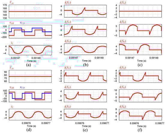
Figure 12.
Simulation results of backward mode with different voltage gain M: (a–c) ; (d–f) .
4.3. Experiment Results
To validate the effectiveness of the presented H-DBRC with the VMM strategy, a 200 W prototype is designed. Figure 13 shows the experimental prototype, which can be divided into four parts: the FPGA controller, the primary-side bridge, the HF transformer and LC resonant tank, and the secondary-side bridge. The key parameters of the prototype are listed in Table 3. The primary-side MOSFETs () are SIHP10N40D and the secondary-side MOSFETs () are IPP320N20N3. consists of a transformer leakage inductor and an external inductor.
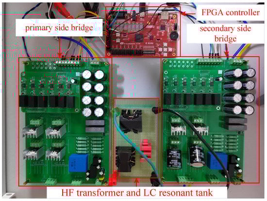
Figure 13.
Picture of the designed converter.
Table 3.
Parameters of the Experiment.
The experimental waveforms under different power levels are presented in Figure 14, Figure 15, Figure 16 and Figure 17 for different voltage gains. In each case, the waveforms recorded from top to bottom are , , resonant current and resonant capacitor voltage , respectively. As shown in Figure 14, when , the waveforms obtained from experimental tests match the simulation plots. ZVS operation of all switches is realized during full power range. H-DBRC functions as a half bridge converter and resonant capacitor absorbs half of the primary side dc voltage. Thus, it can be found that has a dc offset of 75 V. The converter operates in low circulating current situation. The RMS value of at W, 150 W, 100 W, 50 W are 3.67 A, 2.39 A, 1.58 A, and 0.79 A, respectively, which is consistent with the theoretical data. The experimental waveforms for with different power levels are shown in Figure 15. The dc bias is also absorbed by resonant capacitor. Since it is a intermediate state, the ZVS range is relatively narrow. It can be seen that all switches can achieve ZVS at W and 150 W, while switches and lose ZVS operation at light load. The RMS values of at different power levels are slightly greater than theoretical values. The reason is that, in this situation, is no longer a square wave. Therefore, the weight of high-order harmonics of increases, which brings more deviations when using FHA. When in Figure 16, the converter operates in full-bridge state. The optimal performance with full ZVS operation and low circulating current is realized. The RMS value of at W, 150 W, 100 W, 50 W are 3.80 A, 2.39 A, 1.58 A, and 0.77 A, respectively, which is consistent with the theoretical data. As shown in Figure 17, the experimental waveforms with different M under W are illustrated, which indicates the converter operates in backward mode. It can be observed that lags in some degrees and is almost antiphase with . All experimental results match the theory and simulation well.
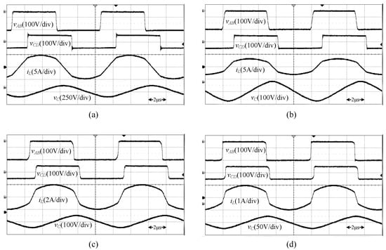
Figure 14.
Experimental waveforms of different power levels when : (a) W, (b) W, (c) W, (d) W.
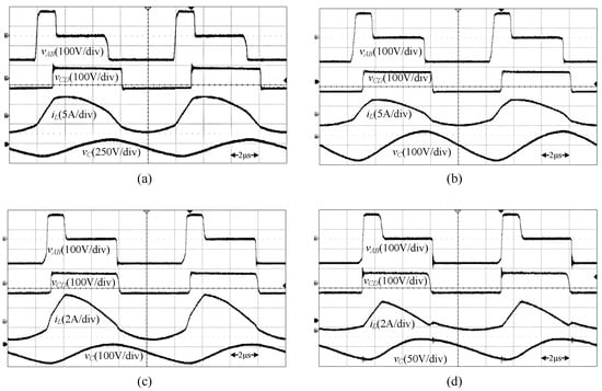
Figure 15.
Experimental waveforms of different power levels when : (a) W, (b) W, (c) W, (d) W.
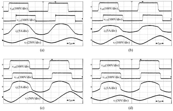
Figure 16.
Experimental waveforms of different power levels when : (a) W, (b) W, (c) W, (d) W.
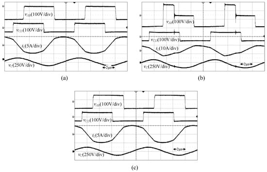
Figure 17.
Experimental waveforms of different M when W: (a) , (b) , (c) .
The conversion efficiency of the H-DBRC with proposed VMM strategy in forward mode are recorded and plotted in Figure 18. It can be seen that the efficiency is almost the same between and , because and are both square waves and the voltages are well matched in the two case. The highest efficiency is at 150 W when . It should be noted that the efficiency decreases in light load, although ZVS operation is always realized. The reason is that the conduction loss is the main part of power loss in light load condition, which may be further reduced by using SiC power transistors.
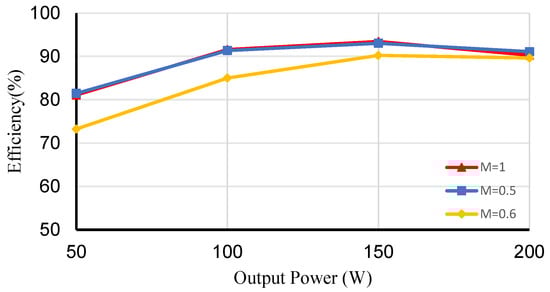
Figure 18.
Measured efficiency at different load levels with different M in forward mode.
Eventually, the H-DBRC with VMM strategy is compared with some previous works, as listed in Table 4, from various perspectives. Excellent performance in many ways is demonstrated in the proposed H-DBRC. It has the minimum number of switches and diodes compared with previous works, which can significantly reduce the economic cost and control complexity. Besides, the voltage range and the ZVS range are broad, under the control of the VMM strategy.
Table 4.
Comparisions between the previous works.
5. Conclusions
In this paper, a H-DBRC with VMM strategy is proposed for wide voltage range applications. The converter can operate in full-bridge state and half-bridge state to realize wide input voltage operation without adding any auxiliary circuit. As a result, it has significant advantages: (1) Low cost and simple control of a simple circuit. (2) The converter can always keep voltage match, and the voltage gain M expands from 1 to 0.5 with high performance. (3) At and , optimum ZVS operation and minimal circulating current are realized. (4) The bidirectional power flow could be achieved with similar effects and the steady-state solution for both forward and backward modes could be obtained uniformly. The operation principle, soft-switching characteristics, and component design are analyzed in detail in this paper. A 200 W prototype is designed to validate the proposed converter and modulation scheme. The converter operates at 100 kHz with a varying input voltage from 75 V to 150 V and an output voltage of 100 V. A maximum efficiency of 93.43% is obtained when . Due to the wide voltage range operation, the efficiency decreases at light load with high conduction loss. Therefore, the selection of power devices and the design of the magnetic components are very important, which require further investigation in the future.
Author Contributions
Conceptualization, S.H.; data curation, Y.L.; formal analysis, R.W.; funding acquisition, S.H.; investigation, W.C. and G.L.; methodology, R.W. and S.H.; software, Y.L.; supervision, X.L.; validation, C.S.; visualization, C.S.; writing—original draft, R.W.; writing—review and editing, S.H. All authors have read and agreed to the published version of the manuscript.
Funding
This research was funded in part by National Natural Science Foundation of China under Grant No. 62003057, in part by FDCT under Grant No. 0065/2019/A2, in part by Natural Science Foundation of Jiangsu Province under Grant No. BK20191029, and in part by the Natural Science Foundation of Jiangsu Higher Education Institutions of China under Grant No. 17KJB510002.
Conflicts of Interest
The authors declare no conflict of interest.
References
- Affam, A.; Buswig, Y.M.; Othman, A.K.B.H.; Julai, N.B.; Qays, O. A Review of Multiple Input DC-DC Converter Topologies Linked with Hybrid Electric Vehicles and Renewable Energy Systems. Renew. Sustain. Energy Rev. 2021, 135, 110186. [Google Scholar] [CrossRef]
- Zhou, X.; Sheng, B.; Liu, W.; Chen, Y.; Wang, L.; Liu, Y.F.; Sen, P.C. A High-Efficiency High-Power-Density On-Board Low-Voltage DC–DC Converter for Electric Vehicles Application. IEEE Trans. Power Electron. 2021, 36, 12781–12794. [Google Scholar] [CrossRef]
- Faisal, M.; Hannan, M.A.; Ker, P.J.; Hussain, A.; Mansor, M.B.; Blaabjerg, F. Review of Energy Storage System Technologies in Microgrid Applications: Issues and Challenges. IEEE Access 2018, 6, 35143–35164. [Google Scholar] [CrossRef]
- Liu, C.; Liu, C.; Cai, G.; Ying, H.; Zhang, Z.; Shan, R.; Pei, Z.; Song, X. An Isolated Modular Multilevel Converter (I-M2C) Topology Based on High-Frequency Link (HFL) Concept. IEEE Trans. Power Electron. 2020, 35, 1576–1588. [Google Scholar] [CrossRef]
- Wu, J.; Li, X.; Zhou, S.; Hu, S.; Chen, H. Constant-Current, Constant-Voltage Operation of a Dual-Bridge Resonant Converter: Modulation, Design and Experimental Results. Appl. Sci. 2021, 11, 12143. [Google Scholar] [CrossRef]
- Lu, M.; Li, X. Performance Evaluation of a Semi-Dual-Active-Bridge with PPWM Plus SPS Control. Electronics 2018, 7, 184. [Google Scholar] [CrossRef]
- Song, W.; Hou, N.; Wu, M. Virtual Direct Power Control Scheme of Dual Active Bridge DC–DC Converters for Fast Dynamic Response. IEEE Trans. Power Electron. 2018, 33, 1750–1759. [Google Scholar] [CrossRef]
- Zhao, B.; Song, Q.; Liu, W.; Sun, Y. Overview of Dual-Active-Bridge Isolated Bidirectional DC–DC Converter for High-Frequency-Link Power-Conversion System. IEEE Trans. Power Electron. 2014, 29, 4091–4106. [Google Scholar] [CrossRef]
- Hou, N.; Li, Y.W. Overview and Comparison of Modulation and Control Strategies for a Nonresonant Single-Phase Dual-Active-Bridge DC–DC Converter. IEEE Trans. Power Electron. 2020, 35, 3148–3172. [Google Scholar] [CrossRef]
- Shi, H.; Wen, H.; Chen, J.; Hu, Y.; Jiang, L.; Chen, G.; Ma, J. Minimum-Backflow-Power Scheme of DAB-Based Solid-State Transformer with Extended-Phase-Shift Control. IEEE Trans. Ind. Appl. 2018, 54, 3483–3496. [Google Scholar] [CrossRef]
- Sun, C.; Li, X. Fast Transient Modulation for a Step Load Change in a Dual-Active-Bridge Converter with Extended-Phase-Shift Control. Energies 2018, 11, 1569. [Google Scholar] [CrossRef]
- Taylor, A.; Liu, G.; Bai, H.; Brown, A.; Johnson, P.M.; McAmmond, M. Multiple-Phase-Shift Control for a Dual Active Bridge to Secure Zero-Voltage Switching and Enhance Light-Load Performance. IEEE Trans. Power Electron. 2018, 33, 4584–4588. [Google Scholar] [CrossRef]
- Guo, Z.; Li, M. An Optimized DPS Control Strategy for LCL Resonant Dual Active Bridge Converter for Wide Voltage Conversion Ratio. IEEE J. Emerg. Sel. Top. Ind. 2021, 2, 501–512. [Google Scholar] [CrossRef]
- Chen, G.; Li, X.; Zhou, S. Unified Boundary Control with Phase Shift Compensation for Dual Bridge Series Resonant DC-DC Converter. IEEE Access 2020, 8, 131137–131149. [Google Scholar] [CrossRef]
- Mu, S.; Guo, Z.; Luo, Y. Universal Modulation Scheme To Suppress Transient DC Bias Current in Dual Active Bridge Converters. IEEE Trans. Power Electron. 2021, 37, 1322–1333. [Google Scholar] [CrossRef]
- Shi, H.; Wen, H.; Chen, J.; Hu, Y.; Jiang, L.; Chen, G. Minimum-Reactive-Power Scheme of Dual-Active-Bridge DC–DC Converter with Three-Level Modulated Phase-Shift Control. IEEE Trans. Ind. Appl. 2017, 53, 5573–5586. [Google Scholar] [CrossRef]
- Li, Y.; Hu, J.; Chen, F.; Li, Z.; He, Z.; Mai, R. Dual-Phase-Shift Control Scheme with Current-Stress and Efficiency Optimization for Wireless Power Transfer Systems. IEEE Trans. Circuits Syst. I Regul. Pap. 2018, 65, 3110–3121. [Google Scholar] [CrossRef]
- Xu, G.; Li, L.; Chen, X.; Liu, Y.; Sun, Y.; Su, M. Optimized EPS Control to Achieve Full Load Range ZVS with Seamless Transition for Dual Active Bridge Converters. IEEE Trans. Ind. Electron. 2021, 68, 8379–8390. [Google Scholar] [CrossRef]
- Carvalho, E.L.; Felipe, C.A.; Bellinaso, L.V.; de Oliveira Stein, C.M.; Cardoso, R.; Michels, L. Asymmetrical-PWM DAB Converter with Extended ZVS/ZCS Range and Reduced Circulating Current for ESS Applications. IEEE Trans. Power Electron. 2021, 36, 12990–13001. [Google Scholar] [CrossRef]
- Hu, S.; Li, X.; Bhat, A.K. Operation of a Bidirectional Series-Resonant Converter with Minimized Tank Current and Wide ZVS Range. IEEE Trans. Power Electron. 2019, 34, 904–915. [Google Scholar] [CrossRef]
- Hu, S.; Li, X.; Zheng, Q.F. A Dual-Bridge DC–DC Resonant Converter Using Extended PWM and Phase-Shift Control. IEEE Trans. Ind. Appl. 2021, 57, 4009–4020. [Google Scholar] [CrossRef]
- Liu, P.; Duan, S. A Hybrid Modulation Strategy Providing Lower Inductor Current for the DAB Converter with the Aid of DC Blocking Capacitors. IEEE Trans. Power Electron. 2020, 35, 4309–4320. [Google Scholar] [CrossRef]
- Pan, X.; Li, H.; Liu, Y.; Zhao, T.; Ju, C.; Rathore, A.K. An Overview and Comprehensive Comparative Evaluation of Current-Fed-Isolated-Bidirectional DC/DC Converter. IEEE Trans. Power Electron. 2020, 35, 2737–2763. [Google Scholar] [CrossRef]
- Mohammed, S.A.Q.; Jung, J.W. A State-of-the-Art Review on Soft-Switching Techniques for DC–DC, DC–AC, AC–DC, and AC–AC Power Converters. IEEE Trans. Ind. Inform. 2021, 17, 6569–6582. [Google Scholar] [CrossRef]
- Hu, S.; Li, X. Performance Evaluation of a Semi-Dual-Bridge Resonant DC/DC Converter with Secondary Phase-Shifted Control. IEEE Trans. Power Electron. 2017, 32, 7727–7738. [Google Scholar] [CrossRef]
- Wu, H.; Chen, L.; Xing, Y. Secondary-Side Phase-Shift-Controlled Dual-Transformer-Based Asymmetrical Dual-Bridge Converter with Wide Voltage Gain. IEEE Trans. Power Electron. 2015, 30, 5381–5392. [Google Scholar] [CrossRef]
- Xu, G.; Sha, D.; Xu, Y.; Liao, X. Hybrid-Bridge-Based DAB Converter with Voltage Match Control for Wide Voltage Conversion Gain Application. IEEE Trans. Power Electron. 2018, 33, 1378–1388. [Google Scholar] [CrossRef]
- Lin, B.R.; Zhuang, Y.Y. Analysis and Implementation of a Hybrid DC Converter with Wide Voltage Variation. Appl. Sci. 2021, 11, 10211. [Google Scholar] [CrossRef]
- Deng, J.; Wang, H. A Hybrid-Bridge and Hybrid Modulation-Based Dual-Active-Bridge Converter Adapted to Wide Voltage Range. IEEE J. Emerg. Sel. Top. Power Electron. 2021, 9, 910–920. [Google Scholar] [CrossRef]
- Khan, S.; Sha, D.; Jia, X.; Wang, S. Resonant LLC DC–DC Convert. Employing Fixed Switch. Freq. Based Dual-Transform. Wide Input-Volt. Range. IEEE Trans. Power Electron. 2020, 36, 607–616. [Google Scholar] [CrossRef]
- Wang, L.; Wang, H.; Xue, B.; Zhou, M. H5-Bridge-Based Single-Input–Dual-Output LLC Converter Wide Output Volt. Range. IEEE Trans. Ind. Electron. 2022, 69, 7008–7018. [Google Scholar] [CrossRef]
- Lin, B.R.; Chen, K.Y. Hybrid LLC Converter with Wide Range of Zero-Voltage Switching and Wide Input Voltage Operation. Appl. Sci. 2020, 10, 8250. [Google Scholar] [CrossRef]
Publisher’s Note: MDPI stays neutral with regard to jurisdictional claims in published maps and institutional affiliations. |
© 2022 by the authors. Licensee MDPI, Basel, Switzerland. This article is an open access article distributed under the terms and conditions of the Creative Commons Attribution (CC BY) license (https://creativecommons.org/licenses/by/4.0/).