Article

Analysis and Design of a High-Frequency Isolated Dual-Transformer DC-DC Resonant Converter

1
School of Mechanical Engineering, Yancheng Institute of Technology, Yancheng 224051, China
2
School of Electrical Engineering and Automation, Changshu Institute of Technology, Suzhou 215000, China
3
Department of Electronic and Information Engineering, The Hong Kong Polytechnic University, Hong Kong 999077, China
4
Faculty of Innovation Engineering, Macau University of Science and Technology, Macau 999078, China
*
Author to whom correspondence should be addressed.
Electronics 2023, 12(1), 103; https://doi.org/10.3390/electronics12010103
Submission received: 30 November 2022 / Revised: 17 December 2022 / Accepted: 22 December 2022 / Published: 27 December 2022

Abstract

:
This paper presents the operation, analysis, design, simulation, and experimental results for a proposed Dual-Transformer DC-DC Resonant Converter (DTRC). A three-arm bridge is employed on the input side and an H-type bridge is employed on the output side of the DTRC, and the two bridges are connected with two high-frequency (HF) transformers. By optimizing the ratio k of the two HF transformers, the proposed DTRC has a lower boundary power for losing zero-voltage switching (ZVS). That means the DTRC has a wider ZVS operation range and lower switching loss when compared with a traditional soft-switching pulse width modulation (PWM) resonant converter. The operation principle, power transfer, ZVS characteristics, and design procedures are analyzed in detail. Both simulation and experimental results prove the feasibility and superiority of the proposed Dual-Transformer DC-DC Resonant Converter.

1. Introduction

An isolated DC-DC power converter is an essential part of the power systems applied in many fields, such as electric vehicles, energy storage systems, and distribution systems [1]. For these applications, an isolated DC-DC power converter can meet the requirements of galvanic isolation and power conversion [2,3]. Among various isolated DC-DC power converter topologies, high-frequency (HF) soft-switching pulse-width-modulation (PWM) DC-DC converters have become a universal solution due to their advantages such as low conduction loss, high power density, and high efficiency [4,5].
As bidirectional soft-switching PWM DC-DC converters, dual active bridge (DAB) converters are the most appealing due to their symmetrical topology, relatively simple structure, and inherent features. Many modulation schemes have been proposed for DAB converters, such as single-phase-shift modulation (SPS) and multi-phase-shift modulation (MPS). With more degrees of freedom and independent control variables of these modulation methods, control strategies for different optimization goals have been reported [6,7], such as minimum reactive current and power [8,9], minimum conduction loss [10], and a full power operation range for soft switching [11]. Nevertheless, the power calculation of these optimization methods is complex, and the operational mode is variable. Depending on the fundamental optimal method-based universal mode [12], a duty cycle modulation is proposed in [13]. Although the calculation becomes less complex, the soft-switching range is limited when the converter operation gain is nonoptimal. Simplified control strategies conflict with a wide zero-voltage switching (ZVS) range for traditional DC-DC resonant converters. Thus, a modified topology of the conventional DAB is proposed in [14] to widen the ZVS range. However, the adopted hybrid control method is also complex.
Apparently, these topologies and control strategies are complicated and cannot solve problems effectively. Another soft-switching PWM resonant topology, L L C resonant converters, have received more attention due to ZVS being achievable for switches and zero-current switching (ZCS) being realizable for diodes. For an L L C resonant converter, the soft-switching operation of all the switches and rectifier diodes can be achieved when designed in a proper working area [15,16,17]. Nevertheless, the circulation current will be enormous if the switching frequency operates far from the resonant frequency, narrowing the voltage regulation range and influencing performance. In [18,19], the related L L C converters are modified to enhance the efficiency over a wide load range, but the topology and control methods are very complex. A backflow power analysis method was proposed in [20] to increase the efficiency of L L C resonant converter. Based on the analysis of the internal relationship between the converter variables, the method can reduce the backflow power by optimizing the resonant parameters. However, the method neglects the influence of the magnetizing current during the deadtime. This results in the switches not meeting ZVS in the designed region. In [21], a combination control scheme of pulse frequency modulation (PFM) and SPS was proposed to ensure operation over a wide range. Furthermore, the paper also proposed a burst-mode control to maintain performance under light-load conditions. Nevertheless, the regulation capability of the hybrid control weakens at light load, and the proposed control method is complex in the reverse mode of an L L C resonant converter. Therefore, an L L C resonant converter with an auxiliary capacitor was proposed to improve the regulation capability in [22]. However, the influence of the coupling was ignored. In [23], a dual half-bridge L L C resonant converter was proposed to increase the efficiency. By making two resonant tanks work in different modes, ZVS for primary switches and ZCS for secondary diodes are achieved over the full power range. Nevertheless, the paper does not take into account the problem of the balance and equalization between two resonant tanks.
The concept of dual-transformer DC-DC converters has spread over the years [24,25,26,27,28]. In [24], a fixed-frequency dual-transformer L L C converter was studied. The converter can suppress the peak current and widen the ZVS operating range. However, there is always a high circulation current in the system, which causes high conduction loss. In [25], the dual-transformer structure can ensure soft switching under a wide range of loads. Nevertheless, the active switches cannot achieve their ZVS at light load when operating in buck mode. For this, an improved topology and optimized modulation method [26] were provided to make sure the converter operates stably in buck-boost mode. However, the power density becomes very low due to the complicated secondary side circuit. Further, the ZVS conditions were not improved either. A dual-transformer converter with discontinuous conduction mode operation is reported in [27] to reduce the filter size and improve performance. Additionally, in [28], a control law was proposed to simplify the topology structure and to reduce the degrees of freedom. Although most switches can achieve a wide ZVS range, the ZVS range of switches on the primary side is limited in reverse mode, and conduction loss is increased.
This paper proposes a new dual-transformer topology to improve the performance. The voltage stress on the transformers is greatly decreased by disassembling an HF transformer into two HF transformers. The current stress and backflow power on the secondary side are naturally minimized due to the topology structure. By optimizing the ratio k of two HF transformers, the proposed DTRC has a lower boundary output power of losing ZVS. Therefore, the ZVS operation range of the converter is widened, resulting in reduced switching loss and increased efficiency. Compared to a traditional soft-switching PWM resonant converter, the performance of the proposed converter is much better. The outline of the paper is as follows. Section 2 presents the topology and the operating principle of the proposed converter. Section 3 describes the steady-state analysis and the ZVS switching constraints to obtain the power transfer characteristics. In Section 4, the selection and design of the parameters with detailed procedures are given. Finally, simulation and experimental results from actual tests on a prototype converter are provided in Section 5.

2. Topology Details and Operation of the DTRC

The proposed Dual-Transformer DC-DC Resonant Converter (DTRC) consists of a three-arm-bridge circuit and an H-bridge circuit, as shown in Figure 1. On the primary side, it has four active switches M A M D , and each switch has a body diode ( d A d D ) and a parasitic capacitor ( C M A C M D ). In addition, the three-arm bridge can be seen as two identical half-bridge circuits. Four diodes d 1 d 4 form the H-bridge circuit on the secondary side. The three-arm bridge and H-type bridge are connected by two HF transformers, T 1 and T 2 . On the primary side of T 1 and T 2 , two identical half-bridge circuits are connected in parallel. The neutral voltage point is shared by two half-bridge circuits and two capacitors, C 1 and C 2 . The resonant tank ( L r and C r ) is connected in series on the secondary side of T 1 and T 2 . The currents of two half-bridge circuits reflected on the secondary side are equal to the resonant current i r due to the series connection on the secondary side. The turns ratio of T 1 is n 1 : 1, while T 2 is n 2 : 1.
The steady-state operation waveforms of the DTRC are shown in Figure 2. Fixed-switching-frequency gating signals with 50% duty cycle are given to switches M A M D . Switches M A , M B , and M C , M D are complementarily conducted, i.e., switching signals on the same bridge arm are 180° out of phase. The mid-point voltages v x z and v y z are generated by the parallel connection. Their amplitudes are equal to V H /2. Phase-shifted gating signals are given to arm M C , M D , causing a phase-shifted angle α between the voltages v x z and v y z . The output voltage V L can be regulated by changing the phase-shift angle α . Due to four diodes forming the circuit, rectification is realized naturally on the secondary side of the DTRC. Thus, the resonant current i r is in phase with the voltage v m n . The voltage v m n generated on the secondary side lags behind the mid-point voltage v x z by phase-shift angle γ , which is defined as the time delay from the rising edge of M A to the zero-crossing point of i r .
As shown in Figure 2, there are six operation intervals in one switching cycle. The equivalent circuits for these intervals are shown in Figure 3. For convenience, several assumptions are made: (1) All the active and passive components and HF transformers are ideal. (2) The dead-gap effect and effects of all parasitic capacitors ( C M A C M D ) are neglected. (3) Residual capacitors ( C H , C 1 , C 2 , C L ) are large enough to maintain the voltages.
Interval 1 ( t 0 t 1 ) (Figure 3a): Before t 0 , switches M B and M D were conducted. At t = t 0 , M B is turned off and M A is turned on. The current flows through d A . The resonant current i r is negative and increases gradually. On the secondary side, the resonant current flows through diodes d 2 and d 3 ; therefore, the voltages v x z = + V H /2, v y z = V H /2, v m n = V L . This interval ends when M D is turned off and M C is turned on.
Interval 2 ( t 1 t 2 ) (Figure 3b): In this interval, M D is turned off and M C is turned on. The resonant current i r is constantly negative and gradually increasing. Meanwhile, it flows through diodes d 2 and d 3 . Therefore the voltage v m n = V L . The currents flow through d A and d C on the primary side. The mid-point voltages v x z = + V H /2, v y z = + V H /2. This interval ends when i r reaches 0.
Interval 3 ( t 2 t 3 ) (Figure 3c): Compared with Interval 2, the resonant current changes the polarity in this interval. It increases from 0 to positive and flows through diodes d 1 and d 4 . The switch currents become positive and flow through M A and M C , so the voltages v x z = + V H /2, v y z = + V H /2, v m n = + V L . This interval ends when M A is turned off and M B is turned on.
Interval 4 ( t 3 t 4 ) (Figure 3d): This interval begins when M A is turned off and M B is turned on forcibly. The current is shifted from M C to d B , which enables the zero-voltage turn-on of M B . There is no change on the secondary side except for a gradual decrease in the resonant current. The voltages v x z = V H /2, v y z = + V H /2, v m n = + V L . This interval lasts until M C is turned off and M D is turned on.
Interval 5 ( t 4 t 5 ) (Figure 3e): The new interval begins when the gating signal of M C is removed. M D is turned on with ZVS. There is still no change on the primary side. The voltages v x z = V H /2, v y z = V H /2, v m n = + V L . At the end of this interval, t = t 5 , and the resonant current reaches 0.
Interval 6 ( t 5 t 6 ) (Figure 3f): Although the resonant current reached 0 at the end of the last interval, M B and M D remain turned on. On the secondary side, the resonant current decreases and flows through d 2 and d 3 . The diodes d 1 and d 4 are turned off with ZCS. The voltages v x z = V H /2, v y z = V H /2, v m n = V L . This interval ends when M B is turned off and M A is turned on. This completes the operation of the DTRC in one switching cycle.

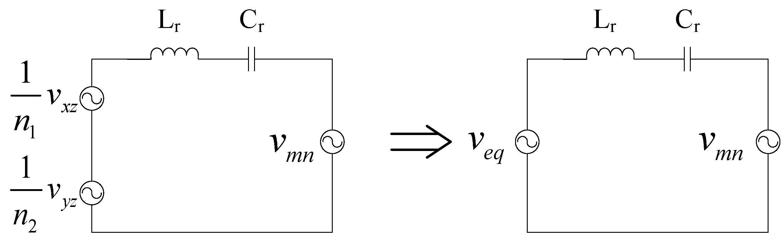
3. Steady-State Analysis and the ZVS Regions of the DTRC

3.1. Steady-State Analysis

To simplify the calculation, the fundamental harmonics approximation (FHA) approach is used due to the nearly sinusoidal waveforms of voltages/currents in the DTRC. Further, parameters on the primary side of HF transformers are transferred to the secondary side for ease of analysis. It is assumed that all of the active and passive components and HF transformers are ideal, and the dead-gap effect is ignored, too. To make analysis more convenient, all parameters are normalized using the following base values:
V B = V H n 1 ;   Z B = R L ;   I B = V B Z B ;   ω B = ω r = 1 L r C r
where R L = V L 2 / P r is the full-load resistance on the secondary side, and P r is the rated power. The turns ratios of two HF transformers are n 1 : 1 and n 2 : 1, respectively, and the parameter k is defined as k = n 2 / n 1 . The voltage gain M of the DTRC is defined as:
M = n 1 V L V H
The normalized values of reactance can be shown as:
X L r , p u = Q F , X C r , p u = Q F
where F = ω s / ω r , Q = ω r L r / R L are the normalized switching frequency and quality factor, respectively.
The FHA equivalent circuit of the DTRC is given in Figure 4. For the resonant tank attached on the secondary side, it is more convenient that the mid-point voltages v x z and v y z reflect onto the secondary side. The normalized expressions of the reflected voltage sources v x z , p u and v y z , p u are given by:
  v x z , p u ( ω s t ) = 1 n 1 v x z , p u ( ω s t ) = 2 π sin ( ω s t )   v y z , p u ( ω s t ) = 1 n 2 v y z , p u ( ω s t ) = 2 k π sin ( ω s t α )
Defining v e q , p u as the equivalent voltage source of v x z , p u and v y z , p u , it is expressed as:
v e q , p u ( ω s t ) = 2 π 2 k cos α + ( 1 k ) 2 + 1 sin ( ω s t arctan ( 1 k sin α 1 + 1 k cos α ) )
The normalized voltage source v m n , p u is obtained as:
v m n , p u ( ω s t ) = 4 M π sin ( ω s t γ )
According to Figure 4, the normalized resonant current i r , p u is written as:
i r , p u ( ω s t ) = v e q , p u ( ω s t ) v m n , p u ( ω s t ) j ( Q F Q F )
After simplifying the equation, the resonant current is:
i r , p u ( ω s t ) = I r , p u · cos ( ω s t + i r , p u )
where the peak value of the resonant current I r , p u and the phase angle i r , p u are shown as follows:
  I r , p u = 2 π ( Q F Q F ) 4 M 2 4 M 1 k cos ( γ α ) 4 M cos γ + 2 k cos α + ( 1 k ) 2 + 1   i r , p u = arctan ( 2 M sin γ 1 k sin α 1 + 1 k cos α 2 M cos γ )
Thus, the normalized output power can be expressed as:
P L , p u = 4 M π 2 ( Q F Q F ) ( sin γ + 1 k sin ( γ α ) )
Due to the diodes’ rectification on the secondary side, the resonant current i r is in phase with the voltage v m n . Thus, the resonant current i r equals zero at t 2 :
i r , p u ( ω s t 2 ) = i r , p u ( γ ) = 0
which means the phase angle of i r is equal to γ + π 2 :
i r , p u = γ + π 2
Then, the relationship between α , γ and M can be expressed as:
2 M = cos γ + 1 k cos ( γ α )
Combining (10) with (13), the normalized output power can be calculated as (14). It is clear that the value of the output power is controlled only by the phase-shifted angle α .
P L , p u = 4 M π 2 ( Q F Q F ) ( 1 k ) 2 + 2 k cos α 4 M 2 + 1

3.2. ZVS Region

The essential condition of ZVS operation for each switch is that the switch current ought to be negative when the switch is turned on. To achieve ZVS, the resonant current should be negative for M A and M C while positive for M B and M D at the turn-on moment. Thus, the ZVS constraints for the switches M A M D of the DTRC are simplified as follows: ZVS of M A and M C requires i r < 0, while that of M B and M D requires i r > 0. The constraints can be expressed as follows:
i r ( t 0 ) < 0 i r ( t 1 ) < 0 i r ( t 3 ) > 0 i r ( t 4 ) > 0 i r ( t 0 ) = i r ( t 3 ) < 0 i r ( t 1 ) = i r ( t 4 ) < 0
Then, the ZVS conditions for the switches of the DTRC are summarized in Table 1.
The ZVS operation regions for the trajectory of the output power transfer are shown in Figure 5. The red line represents the ZVS operation boundary of M A , M B , and the cyan line is the boundary of M C , M D . The region where switches M A M D will lose ZVS are marked in the figure. The black line represents the trajectory of the power transfer. The blue intersection of three lines indicates the zero power, i.e., P L = 0. It can be seen that the power point is moving away from the ZVS boundary of M A , M B with the increasing power level, which means the switches M A and M B always work in ZVS operation. Meanwhile, part of the black line is in the area where M C and M D lose ZVS. That means M C and M D will lose ZVS at partial loads.

4. Design Procedures

4.1. Selection of k

From the steady-state and ZVS region analysis, it is found that the proposed DTRC operates as the conventional soft-switching PWM resonant converter when k = 1. In order to compare the performances of the DTRC and the PWM converter, the total loss of two converters is analyzed next.
The total loss of the resonant converter is mainly divided into two aspects: the conduction loss and the switching loss. Combining (9) with (13), the normalized root mean square (RMS) value of resonant current I r , r m s , p u can be expressed as:
I r , r m s , p u = 2 2 π ( Q F Q F ) ( 1 k ) 2 + 2 k cos α 4 M 2 + 1
From (14) and (16), the relationship between the output power and the RMS value of the resonant current is shown as (17):
I r , r m s , p u = 2 π · P L , p u 4 M
It can be seen that the RMS value of resonant currents through the DTRC and the PWM converter will be the same if they have the same output power P L ; so the different values of k do not affect the RMS value of resonant current. Therefore, there is no apparent difference in conduction loss between the DTRC and the PWM converter.
Consequently, the switching loss becomes the principal portion of the total loss for two converters. Due to the diodes’ circuit on the secondary side, the operation of the converter must meet the requirement of expression (13), i.e., the diodes’ rectification. According to Figure 5, it is possible to lose ZVS of the switches M C and M D at light load for two converters. Thus, the boundary output power of losing ZVS for each converter can be predicted by the following conditions:
2 M cos ( γ α ) cos α 1 k = 0 2 M = cos γ + 1 k cos ( γ α )
Then, the boundary output power of losing ZVS for the proposed DTRC is expressed as:
P L , Z V S , p u = 4 M π 2 ( Q F Q F ) 1 ( 2 M 1 k ) 2
When k = 1, the DTRC works as the PWM converter. Let k be equal to 1 in expression (19), the boundary output power of losing ZVS for the traditional PWM converter can be simplified as:
P t , Z V S , p u = 8 M π 2 ( Q F Q F ) M M 2
Once the voltage gain M is determined, the boundary output power of losing ZVS for the traditional PWM converter is specific while uncertain for the DTRC due to k. Thus, the performance of the DTRC is decided by k. Set D as the ratio of the boundary output power of losing ZVS between the DTRC and the traditional PWM converter as follows:
D = 2 M M 2 1 ( 2 M 1 k ) 2
Taking M = 0.5 as an example, the relationship between D and different k is shown in Figure 6. According to (21), D > 1 means the boundary output power of losing ZVS for the DTRC is lower than that for the PWM converter. That means the DTRC has a wider ZVS operation range when D > 1. As shown in Figure 5, the ZVS constraint of switches M C is the same as M D for the DTRC and the traditional PWM resonant converter. Even at 50% load, it is possible for M C and M D to lose their ZVS. The values of D represent the multiple of the boundary output power of the PWM converter. For example, if the ZVS boundary power of the PWM converter is 100 W when D = 2, the boundary power of the DTRC will only be 50 W. According to expression (21), the value of D will be large enough at k = 0.5, which means the DTRC can hardly lose ZVS. In order to validate the above analysis, M = 0.5, k = 0.5 are selected to compare the switching loss (ZVS operation) of the DTRC and traditional soft-switching PWM converter.
Figure 7 shows the variation ranges of P L , p u and α when M and k change. Once M and k are determined, the normalized output power P L , p u will only be regulated by the phase angle α according to (14). Figure 7 demonstrates that the DTRC has a broader operating range and more extensive power range when M = 0.5, k = 0.5. It also can be found that the peak output power when M = 0.5, k = 0.5 is always greater than others. Therefore, in this case, the output power of DTRC can be easily regulated.

4.2. Design Example

To validate the theoretical analysis of the DTRC, a converter is designed as follows: the rated output power P r = 200 W, input voltage V H = 150 V, output voltage V L = 80 V, switching frequency f s = 100 kHz, and values of M = 0.5, k = 0.5 are chosen. The selection value of the normalized switching frequency F should be greater than one but close to one to regulate ZVS operation of the converter and to reduce the circulation of the switches on the primary side. The appropriate Q value is selected to reduce the resonant current and voltage peak and to improve the power factor. In this paper, Q = 1 and F = 1.4 are chosen.
For the proposed DTRC, V H = 150 V, V L = 80 V, P r = 200 W, f s = 100 kHz, M = 0.5, and k = 0.5. Thus, the turns ratio of T 1 can be calculated by M, and it is shown as follows:
M = n 1 V L V H = 0.5
which turns out to be:
n 1 = M V H V L = 0.9375
Thus, the turns ratio of T 2 can be written as:
n 2 = k n 1 = 0.46875
The base value of the voltage
V B = V H n 1 = 160 V
the load resistance
R B = R L = V L 2 P r = 32 Ω
and the current
I B = V B R B = 5 A
Therefore, the base value of the output power will be:
P B = V B 2 R B = 800 W
The values of the resonant tank are calculated as:
  F = ω s ω r = 2 π f s L r C r = 1.4   Q = ω r L r R L = 1
The values of the resonant tank are solved as:
  L r = 71.3 μ H   C r = 69.63 n F .

5. Simulation and Experimental Results

5.1. Simulation Results

The ZVS region and the power lines of k and α are shown in Figure 8. The switches M A and M B consistently achieve ZVS no matter what the value of k is, as shown in Figure 5. The shaded area represents that M C and M D lose ZVS. The red dashed lines are the power lines of 200 W, 150 W, 100 W, and 50 W, respectively. According to Figure 8, the purple line k = 1 has four intersections with four power lines, and the intersections are all located in the shaded area. That means switches M A and M B achieve ZVS, while M C and M D lose ZVS during the four power conditions when M = 0.5. For the traditional soft-switching PWM converter, i.e., k = 1, switches M C and M D lose ZVS at light load or even half load. The conclusion conforms to how a traditional soft-switching PWM converter performs. For the proposed DTRC, four intersections are located out of the shaded area at k = 0.5. That means all the switches work in ZVS operation under different loads.
To show the relationship more clearly, the comparison between the traditional PWM converter (k = 1) and the DTRC (k = 0.5) is shown in Figure 9. Figure 9a shows the ZVS region and the power lines when k = 1 at M = 0.5. Switches M A , M B continuously meet ZVS when k takes different values. The blue line is the ZVS boundary of switches M C , M D . The area where M C , M D lose ZVS is marked in the figure. The dashed lines in magenta are the different power lines. As shown in Figure 9, the values of α and γ that allow the converter to achieve the required power are restricted due to rectification of the secondary-side H-type bridge, i.e., the green line in the figure. In Figure 9a, four power lines, 200 W, 150 W, 100 W, and 50 W, have four intersections with the rectification path. All of the intersections are located in the areas where M A , M B achieve ZVS while M C , M D lose ZVS when k = 1. In Figure 9b, the intersections are located where M A , M B , M C , and M D all work in ZVS operation when k = 0.5.
In this paper, PSIM software is used to perform the simulation. Simulations are done for four cases: 200 W, 150 W, 100 W, and 50 W. The critical simulation waveforms of the mid-point voltages ( v x z and v y z ), the secondary side square-wave voltage ( v m n ), the resonant current ( i r ), the output current ( i L ), and the currents through four active switches ( M A M D ) and four diodes ( d 1 d 4 ) at k = 0.5 when M = 0.5 are shown in Figure 10, respectively. The output voltage V L is regulated at 80 V. The output current i L realizes the rectification, and the diodes d 1 d 4 achieve ZCS on the secondary side. The switches on the primary side all work in ZVS operation at the four power conditions. All waveforms are matched with what is expected.
The voltages v x z and v y z have a phase shift α , and their amplitudes are V H /2 = 150 V/2 = 75 V. The voltage v m n lags behind v x z a phase-shifted angle γ , and its amplitude is 80 V. The resonant current i r is approximately sinusoidal. Further, Figure 10 demonstrates ZVS for M A M D since their body-parallel diodes conduct before the switches start conducting. For the converter, the current stress decreases with lower power, and the output current i L has almost no circulation during each cycle.

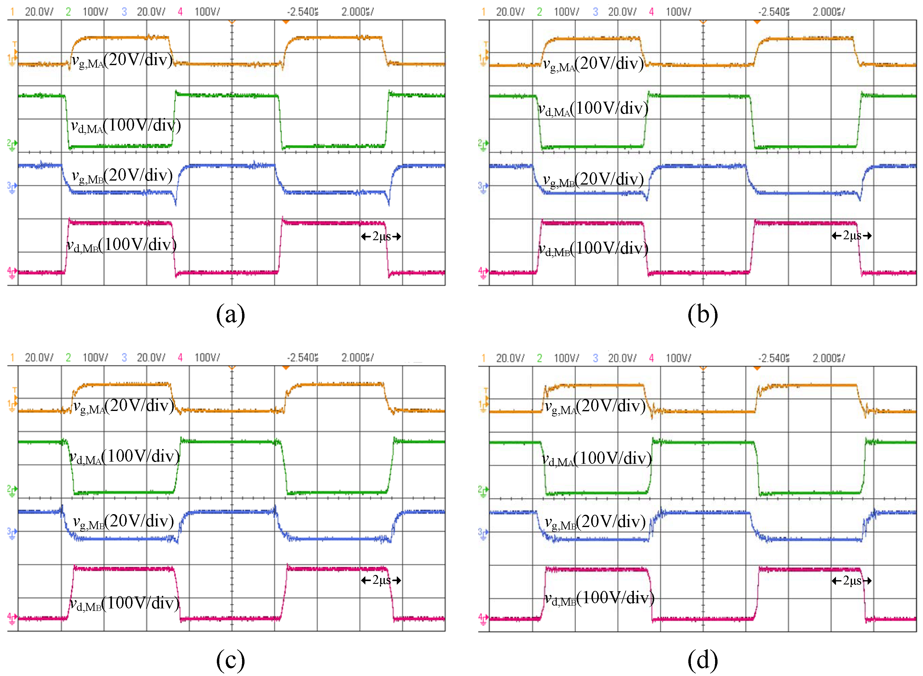
5.2. Experiment Results

A 200 W, 150 V input, 80 V output, switching at 100 kHz, experimental dual-transformer DC-DC resonant converter was built in the laboratory based on the design parameters obtained in Section 4. Some details are provided to verify the performance of the proposed DTRC in the following. Figure 11 shows the experimental prototype divided into four parts: the FPGA controller, the primary and secondary side bridge circuits, the HF transformers, and the L C resonant tank. The critical parameters of the experimental prototype are summarized in Table 2. The control platform is an FPGA development board, in which HF gating signals for the MOSFETs are generated. The resonant inductor L r comprises two transformer leakage inductors and an external inductor.
Figure 12a–d illustrate the gating signals v g , M A v g , M D of the active switches M A M D at different power levels from 100% load to 25% load, respectively. Power devices M A , M B and M C , M D work complementarily with a fixed duty cycle of 0.5. Figure 13 provides the measured results of mid-point voltages v x z , v y z and currents i r 1 , i r 2 on the primary side. Figure 13a shows the full-load case. The primary-side full-bridge circuit is seen as two half-bridge circuits. Two capacitors C 1 , C 2 share the midpoint, so the amplitudes of two voltages v x z = v y z = V H /2 = 150 V/2 = 75 V. The current i r 1 is different from i r 2 due to different transformer ratios of the two HF transformers T 1 , T 2 , and the RMS values of resonant currents i r 1 , i r 2 are I r 1 , r m s = 2.84 A, I r 2 , r m s = 5.61 A. The theoretical RMS values are I r 1 , r m s = 2.96 A, I r 2 , r m s = 5.92 A. It can be seen that there is not much difference between the theoretical and experimental results. Figure 13b–d provides the waveforms at 75%, 50%, and 25% load. The amplitudes of the voltages remain.
The RMS values of current i r 1 are 2.13 A, 1.38 A, and 0.73 A, and those of i r 2 are 4.28 A, 2.75 A, and 1.45 A, respectively, which also matches the theoretical values well. Furthermore, it can be observed that the resonant currents are negative for M A and M C while positive for M B and M D at the turn-on moment. That is to say, ZVS operation of all the active switches is achieved at the four power conditions. Figure 14a–d show the tested results of square voltage v m n , capacitor voltage v C r , and resonant current i r on the secondary side when the output power ranges from 200 W to 50 W. The amplitudes of the secondary side voltage v m n are kept at 80 V under different load conditions. The RMS values of resonant current i r at 100% to 25% rated power are 2.67 A, 2.03 A, 1.31 A, and 0.68 A, respectively. The results are almost the same as the theoretical results. The voltage v m n is in phase with the resonant current i r . The capacitor voltage v C r and resonant current i r are nearly sinusoidal, confirming resonance operation. Figure 15a–d demonstrate the gating signals and switch voltages of M A and M B under different loads. The gating signals and switch voltages of M C and M D are not given due to having the same waveforms as M A and M B except for the phase-shift angle α . Load voltage is maintained at 80 V by increasing the phase angle α when the loads are reduced. The operation performance with full ZVS operation and circulation current minimization is realized. All experimental results match the theory and simulation well. The efficiency of the DTRC at four power levels is shown in Figure 16. The recorded efficiencies at 200 W, 150 W, 100 W, and 50 W are 94.02%, 95.36%, 96.16%, and 90.87%, respectively. Since ZVS operation is achieved and switching loss is reduced, the overall efficiency of the DTRC exceeds 90%.
The performance comparison between the proposed DTRC and some converters mentioned in Section 1 is given in Table 3. The degrees of freedom of [14] are more than those of other converters, which causes control complexity. Moreover, the soft-switching conditions are not better than others’ because of the non-resonant structure. The topology of the three-phase two-tank L L C converter [18] and the dual-transformer L L C converter [24] both have two transformers, which is similar to the proposed DTRC. However, the cost is higher due to more switches and inductors.

6. Conclusions

This paper proposes a new Dual-Transformer DC-DC Resonant Converter that features asymmetrical turns ratios of the HF transformers. By setting k as the ratio of two transformers, more freedom was provided to optimize the DTRC. Due to the features of the structure, the converter can operate with low voltage stress and minimal backflow power without any control strategy. Compared with the conventional soft-switching PWM resonant converter, the DTRC can widen the ZVS operation range and reduce the switching loss. Even at a very light load, the DTRC can still keep all active switches working in ZVS operation. Naturally, the backflow power on the output side is almost eliminated. Experimental measurements validated the theoretical analysis and demonstrated the features of the proposed DTRC.

Author Contributions

Conceptualization, S.H.; Methodology, Y.L. and S.H.; Software, R.W.; Validation, C.S.; Formal analysis, Y.L.; Investigation, L.Z. and L.M.; Data curation, R.W.; Writing—original draft, Y.L.; Writing—review and editing, S.H.; Visualization, C.S.; Supervision, X.L.; Funding acquisition, S.H. All authors have read and agreed to the published version of the manuscript.

Funding

This research was funded in part by the National Natural Science Foundation of China under grant No. 62003057, in part by the FDCT under grant No. 0065/2019/A2, in part by the Natural Science Foundation of Jiangsu Province under grant No. BK20191029, and in part by the Natural Science Foundation of Jiangsu Higher Education Institutions of China under grant No. 19KJB470001.

Conflicts of Interest

The authors declare no conflict of interest.

References

  1. Wu, J.; Li, X.; Zhou, S.; Hu, S.; Chen, H. Constant-current, constant-voltage operation of a dual-bridge resonant converter: Modulation, design and experimental results. Appl. Sci. 2021, 11, 12143. [Google Scholar] [CrossRef]
  2. Gunawardena, P.; Nayanasiri, D.; Hou, N.; Li, Y. A Soft-Switched Current-Fed Dual-Input Isolated DC-DC Converter Topology. IEEE Trans. Ind. Electron. 2022, 1–12. [Google Scholar] [CrossRef]
  3. Hong, T.; Geng, Z.; Qi, K.; Zhao, X.; Ambrosio, J.; Gu, D. A wide range unidirectional isolated DC-DC converter for fuel cell electric vehicles. IEEE Trans. Ind. Electron. 2020, 68, 5932–5943. [Google Scholar] [CrossRef]
  4. Hu, S.; Zhang, Y.F.; Li, X. A dual-asymmetric PWM control strategy for full bridge DC-DC converters. In Proceedings of the 2017 12th IEEE Conference on Industrial Electronics and Applications (ICIEA), Siem Reap, Cambodia, 18–20 June 2017; pp. 31–36. [Google Scholar]
  5. Hu, S.; Li, X. An unbalanced PWM control strategy for the full-bridge series resonant converter. In Proceedings of the 2019 14th IEEE Conference on Industrial Electronics and Applications (ICIEA), Xi’an, China, 19–21 June 2019; pp. 2249–2253. [Google Scholar]
  6. Bu, Q.; Wen, H.; Shi, H.; Zhu, Y. A Comparative Review of High-Frequency Transient DC Bias Current Mitigation Strategies in Dual-Active-Bridge DC-DC Converters Under Phase-Shift Modulations. IEEE Trans. Ind. Appl. 2021, 58, 2166–2182. [Google Scholar] [CrossRef]
  7. Hu, S.; Li, X.; Zheng, Q.F. A dual-bridge DC–DC resonant converter using extended PWM and phase-shift control. IEEE Trans. Ind. Appl. 2021, 57, 4009–4020. [Google Scholar] [CrossRef]
  8. Rodriguez-Rodriguez, J.R.; Salgado-Herrera, N.M.; Torres-Jimenez, J.; Gonzalez-Cabrera, N.; Granados-Lieberman, D.; Valtierra-Rodriguez, M. Small-signal Model for Dual-active-bridge Converter Considering Total Elimination of Reactive Current. J. Mod. Power Syst. Clean Energy 2020, 9, 450–458. [Google Scholar] [CrossRef]
  9. Shi, H.; Wen, H.; Hu, Y.; Jiang, L. Reactive power minimization in bidirectional DC–DC converters using a unified-phasor-based particle swarm optimization. IEEE Trans. Power Electron. 2018, 33, 10990–11006. [Google Scholar] [CrossRef]
  10. Guo, Z. Modulation scheme of dual active bridge converter for seamless transitions in multiworking modes compromising ZVS and conduction loss. IEEE Trans. Ind. Electron. 2019, 67, 7399–7409. [Google Scholar] [CrossRef]
  11. Carvalho, E.L.; Felipe, C.A.; Bellinaso, L.V.; de Oliveira Stein, C.M.; Cardoso, R.; Michels, L. Asymmetrical-PWM DAB converter with extended ZVS/ZCS range and reduced circulating current for ESS applications. IEEE Trans. Power Electron. 2021, 36, 12990–13001. [Google Scholar] [CrossRef]
  12. Zhao, B.; Song, Q.; Liu, W.; Liu, G.; Zhao, Y. Universal high-frequency-link characterization and practical fundamental-optimal strategy for dual-active-bridge DC-DC converter under PWM plus phase-shift control. IEEE Trans. Power Electron. 2015, 30, 6488–6494. [Google Scholar] [CrossRef]
  13. Choi, W.; Rho, K.M.; Cho, B.H. Fundamental duty modulation of dual-active-bridge converter for wide-range operation. IEEE Trans. Power Electron. 2015, 31, 4048–4064. [Google Scholar] [CrossRef]
  14. Mou, D.; Yuan, L.; Li, J.; Hou, N.; Li, J.; Li, Y.; Zhao, Z. Modeling and Analysis of Hybrid Dual Active Bridge Converter to Optimize Efficiency over Whole Operating Range. IEEE J. Emerg. Sel. Top. Power Electron. 2022. [Google Scholar] [CrossRef]
  15. Xu, J.; Yang, J.; Xu, G.; Jiang, T.; Su, M.; Sun, Y.; Wang, H.; Zheng, M. PWM modulation and control strategy for LLC-DCX converter to achieve bidirectional power flow in facing with resonant parameters variation. IEEE Access 2019, 7, 54693–54704. [Google Scholar] [CrossRef]
  16. Zhang, J.; Liu, J.; Yang, J.; Zhao, N.; Wang, Y.; Zheng, T.Q. An LLC-LC type bidirectional control strategy for an LLC resonant converter in power electronic traction transformer. IEEE Trans. Ind. Electron. 2018, 65, 8595–8604. [Google Scholar] [CrossRef]
  17. Shi, L.; Liu, B.; Duan, S. Burst-mode and phase-shift hybrid control method of LLC converters for wide output range applications. IEEE Trans. Ind. Electron. 2019, 67, 1013–1023. [Google Scholar] [CrossRef]
  18. Salem, M.; Ramachandaramurthy, V.K.; Jusoh, A.; Padmanaban, S.; Kamarol, M.; Teh, J.; Ishak, D. Three-phase series resonant DC-DC boost converter with double LLC resonant tanks and variable frequency control. IEEE Access 2020, 8, 22386–22399. [Google Scholar] [CrossRef]
  19. Wei, Y.; Luo, Q.; Mantooth, A. Hybrid control strategy for LLC converter with reduced switching frequency range and circulating current for hold-up time operation. IEEE Trans. Power Electron. 2021, 36, 8600–8606. [Google Scholar] [CrossRef]
  20. Shi, Z.; Tang, Y.; Guo, Y.; Li, X.; Sun, H. Optimal Design Method of LLC Half-bridge Resonant Converter Considering Backflow Power Analysis. IEEE Trans. Ind. Electron. 2021, 69, 3599–3608. [Google Scholar] [CrossRef]
  21. Lin, J.Y.; Yueh, H.Y.; Lin, Y.F.; Liu, P.H. Variable-Frequency and Phase-Shift with Synchronous Rectification Advance On-Time Hybrid Control of LLC Resonant Converter for Electric Vehicles Charger. IEEE J. Emerg. Sel. Top. Ind. Electron. 2022. [Google Scholar] [CrossRef]
  22. Yeon, C.O.; Kim, J.W.; Park, M.H.; Lee, I.O.; Moon, G.W. Improving the light-load regulation capability of LLC series resonant converter using impedance analysis. IEEE Trans. Power Electron. 2016, 32, 7056–7067. [Google Scholar] [CrossRef]
  23. Wei, Y.; Luo, Q.; Du, X.; Altin, N.; Nasiri, A.; Alonso, J.M. A dual half-bridge LLC resonant converter with magnetic control for battery charger application. IEEE Trans. Power Electron. 2019, 35, 2196–2207. [Google Scholar] [CrossRef]
  24. Khan, S.; Sha, D.; Jia, X.; Wang, S. Resonant LLC DC–DC converter employing fixed switching frequency based on dual-transformer with wide input-voltage range. IEEE Trans. Power Electron. 2020, 36, 607–616. [Google Scholar] [CrossRef]
  25. Wu, H.; Chen, L.; Xing, Y.; Xiao, X.; Xu, P. Two-transformer-based full-bridge soft-switching DC–DC converter with improved characteristics. IET Power Electron. 2015, 8, 2537–2545. [Google Scholar] [CrossRef]
  26. Wu, H.; Sun, K.; Liu, T.; Xing, Y. Isolated Buck-Boost converters with AC-TLR and dual-transformer structure for wide output voltage range applications. IET Power Electron. 2019, 12, 184–194. [Google Scholar] [CrossRef]
  27. Ning, G.; Chen, W.; Shu, L.; Qu, X. A hybrid ZVZCS dual-transformer-based full-bridge converter operating in DCM for MVDC grids. IEEE Trans. Power Electron. 2016, 32, 5162–5170. [Google Scholar] [CrossRef]
  28. Xu, G.; Sha, D.; Xu, Y.; Liao, X. Dual-transformer-based DAB converter with wide ZVS range for wide voltage conversion gain application. IEEE Trans. Ind. Electron. 2017, 65, 3306–3316. [Google Scholar] [CrossRef]
Figure 1. The topology of the Dual-Transformer DC-DC Resonant Converter.
Electronics 12 00103 g001
Figure 2. The steady-state operation waveforms of the DTRC.
Electronics 12 00103 g002
Figure 3. The equivalent circuits during different intervals of DTRC.
Electronics 12 00103 g003
Figure 4. The FHA equivalent circuit of the DTRC.
Electronics 12 00103 g004
Figure 5. The ZVS operation regions for the trajectory of the power transfer.
Electronics 12 00103 g005
Figure 6. The ratio of the boundary output power for losing ZVS at different values of k.
Electronics 12 00103 g006
Figure 7. The variation ranges of P L , p u and α at different values of M and k.
Electronics 12 00103 g007
Figure 8. The ZVS region and the power lines of k and α .
Electronics 12 00103 g008
Figure 9. The ZVS region and the power lines of α and γ at M = 0.5: (a) k = 1; (b) k = 0.5.
Electronics 12 00103 g009
Figure 10. The key simulation waveforms of the DTRC at k = 0.5 when M = 0.5: (a) 200 W; (b) 150 W; (c) 100 W; and (d) 50 W.
Electronics 12 00103 g010
Figure 11. The experimental prototype of the proposed converter.
Electronics 12 00103 g011
Figure 12. Experimental gating signals v g , M A v g , M D at different power levels: (a) 200 W, (b) 150 W, (c) 100 W, and (d) 50 W.
Electronics 12 00103 g012
Figure 13. Experimental mid-point voltages v x z , v y z and current results i r 1 , i r 2 at different power levels: (a) 200 W, (b) 150 W, (c) 100 W, and (d) 50 W.
Electronics 12 00103 g013
Figure 14. Experimental square voltage v m n , capacitor voltage v C r , and resonant current i r at different power levels: (a) 200 W, (b) 150 W, (c) 100 W, and (d) 50 W.
Electronics 12 00103 g014
Figure 15. Experimental waveforms v g , M A , v d , M A , v g , M B , and v d , M B of M A and M B at different power levels: (a) 200 W, (b) 150 W, (c) 100 W, and (d) 50 W.
Electronics 12 00103 g015
Figure 16. Measured efficiency under four load levels of DTRC.
Electronics 12 00103 g016
Table 1. The ZVS conditions for the switches.
SwitchesZVS Conditions
M A , M B 2 M cos γ 1 k cos α 1 < 0
M C , M D 2 M cos ( γ α ) cos α 1 k < 0
Table 2. Parameters of the prototype.
ParameterValue
Input voltage ( V H )150 V
Output voltage ( V L )80 V
Rated power ( P r )200 W
Switching frequency ( f s )100 kHz
Turns ratio of the transformer T 1 ( n 1 :1)30:32
Turns ratio of the transformer T 2 ( n 2 :1)15:32
Resonant inductor ( L r )71.3  μ H
Resonant capacitor ( C r )69.63 nF
Primary-side switches ( M A M D )C3M0025065D (650 V/97 A)
Secondary-side diodes ( d 1 d 4 )MBR40250G (250 V/40 A)
Table 3. Comparison with other converters.
TopologyHybrid Dual Active Bridge Converter [14]Three-Phase Two-Tanks LLC Converter [18]Dual-Transformer LLC Converter [24]Proposed Dual-Transformer Resonant Converter
Voltage gain0.25∼0.51∼21∼20.5∼1
Control variables4222
Number of MOSFETs6644
Number of diodes0444
Transformers1222
ModulationMPSPFMMPSSPS
Resonant components0422
Soft switchingZVSZVSZVS and ZCSZVS and ZCS
CostMediumHighHighLow
Disclaimer/Publisher’s Note: The statements, opinions and data contained in all publications are solely those of the individual author(s) and contributor(s) and not of MDPI and/or the editor(s). MDPI and/or the editor(s) disclaim responsibility for any injury to people or property resulting from any ideas, methods, instructions or products referred to in the content.

