1. Introduction
To comply with the emerging processing technologies of smart cities, autonomous driving, and AI robots, a tremendous amount of data needs to be efficiently processed [
1,
2,
3,
4,
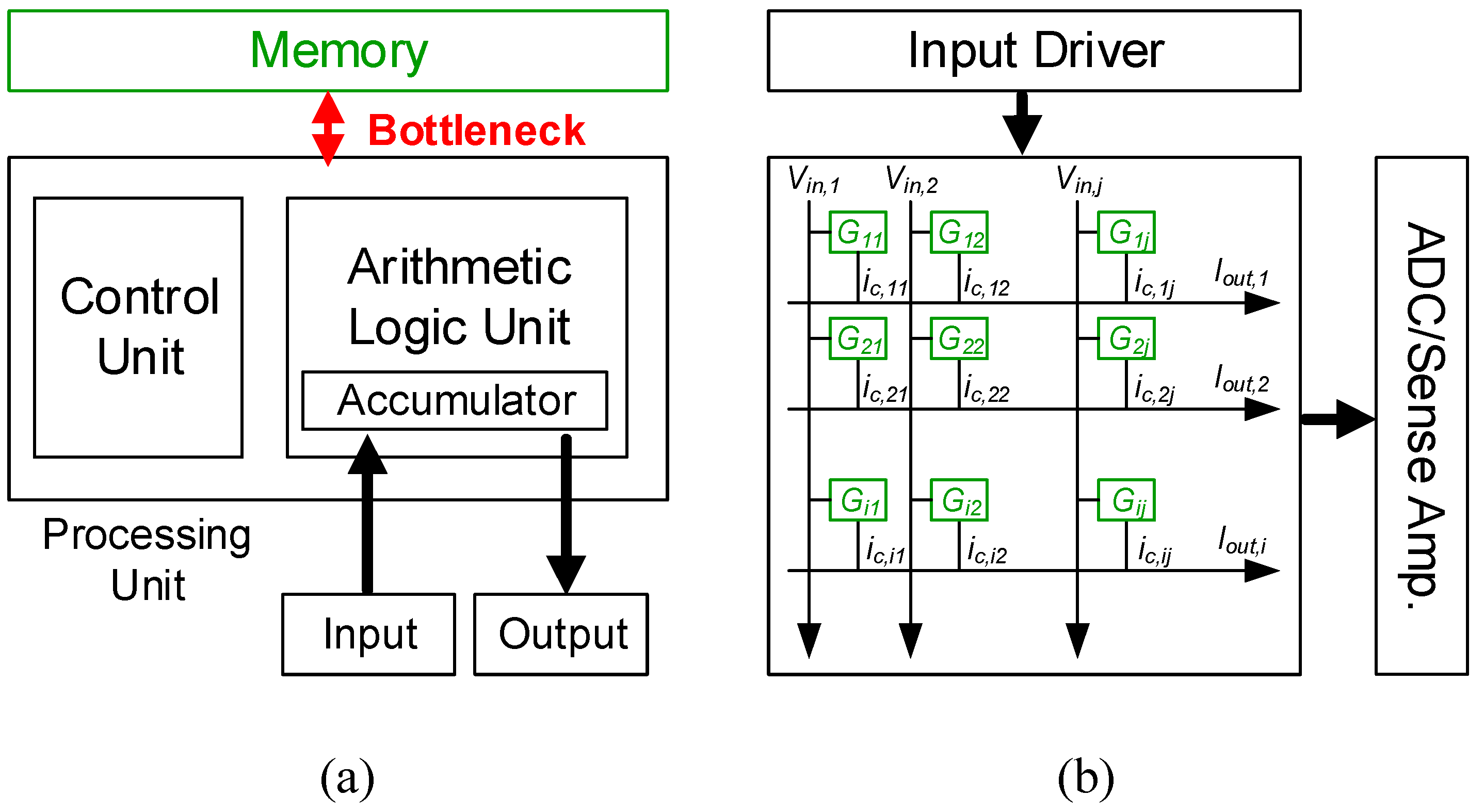
5]. However, the existing von Neumann computing structures shown in
Figure 1a have limitations, because distinct areas are separated for dedicated roles [
1], which causes heavy traffic in data transmission, inducing a significant efficiency drop and vast power consumption [
2]. To overcome these problems, there is a growing interest in “compute-in-memory” (CIM) that mimics the human brain neural network. In CIM, the power efficiency and decision fidelity are significantly improved if multi-level data are processed in parallel and linearity of output is secured [
3]. In the implementation of artificial intelligence, with constructed with secured linearity, neural network structures are suitable for in-memory computing in a cross-bar structure, as shown in
Figure 1b [
4,
5,
6]. The special features of the cross-bar structure are that each cell maintains the weight data in the form of cell conductance (
); the cell current (
) then appears as the product of the analog input voltage (
) and the cell conductance. Each row accumulates the cell current from cells within the row to generate the output current (
), which is the result of the multiply-and-accumulate (MAC) calculation, as shown in Equation (1) [
7].
The MAC calculation in a cross-bar array is the most frequent and important operation of the vector–matrix multiplier (VMM) of neural networks [
8]. The memory element in a neural network VMM has to be the multiplication operator and storage device for the weight factor. If a cell can store multiple levels of states, the MAC performance is enhanced and the power consumption is consequently reduced. The multi-level cells in a VMM array are expected to provide linear characteristics for both the inference and learning modes of the neural network [
9]. The memory cell is read during the inference step, while the memory state is modified during the learning step. Other characteristics required of the multi-level cells for the inference and learning steps are summarized in
Table 1.
Emerging non-volatile memory devices, including resistant random access memory (RRAM), phase change memory (PCM), charge trap transistors (CTTs), ferroelectric field effective transistors (FeFETs), and floating-gate (FG) FETs, have been proposed as promising candidates for neuromorphic cell memory.
Table 2 compares the characteristics of non-volatile memory devices for neuromorphic VMM applications [
10]. It is difficult to achieve linear multiple states of conductance with RRAM and PCM, and modification of the conductance is neither symmetric nor reproducible, because the program and erase functions behave differently. Alternatively, charge storage FETs, such as CTT and FG FET, improve the linearity and symmetry in multiple levels of conductance states when accompanied by an incremental step pulse program (ISPP) technique [
11]. Although the linearity in multiple weight levels is acceptable in charge storage FET devices, the linearity between the input voltage (
) and cell current (
) is not inherent. The linearity quickly deteriorates as the input voltage increases because of the secondary effects of FETs, which limits the narrow input swing range of the operation.
In this paper, we provide a systematic analysis of the linearity between the input voltage and cell current in FET-based neuromorphic VMM cells, and suggest noble cell structures that provide improved linearity over an extended input voltage range. The diminishing current because of the quadratic term of the cell current is compensated for by either boosting the bias on the FET terminals or adding an auxiliary current path in the cell, depending on the type of FET.
2. Linearity Improvement in VMM Cells Based on Floating Gate FETs
2.1. Array Architecture and Cell Candidates
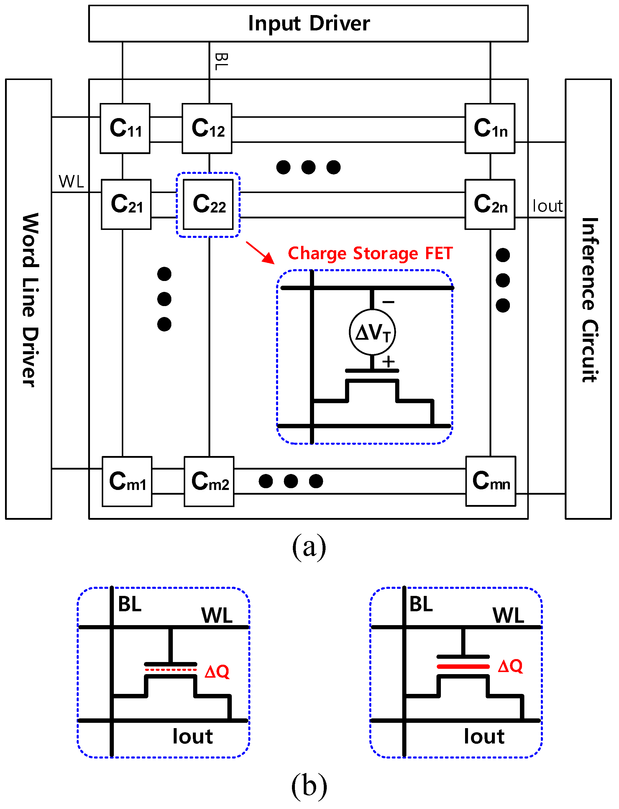
Figure 2a shows the full architecture of VMM using charge storage FET cells. Although the word line driver supplies a constant potential to all gate nodes (WL) of FETs during the inference step, each cell may have a different conductance if the threshold voltage of the cell FET is altered. The drain current of a cell is determined by the cell conductance and input voltage on the drain node (BL). The merged drain current from cells that are attached to a WL enter the inference circuit to prioritize the correlation between the input vector and output vector under the weight matrix. All rows simultaneously drive the output current to perform a flash operation of VMM. The threshold voltage of the FET cells is updated row by row, by applying a large electric field between the selected WL and BLs. Unselected WLs are tied to ground, to avoid unwanted disturbance of the stored states during the training operation of the adjacent rows of the array.
The threshold of FET cells is simply modified by changing the amount of trapped charges between the gate node and channel of the FET, similarly to flash memory cells. Traditionally, flash memory writes/erases data by injecting/removing electrons into/from the conductive floating gate, respectively. However, charge trapped FETs, where the charges are stored in the insulating medium of the gate dielectric, have recently replaced floating gate FETs [
12]. Commercial flash memory products are currently capable of maintaining multiple levels of electron storage in a cell, by changing the amount of trapped charges in the floating gate or gate dielectric.
Figure 2b shows examples of charge storage FET cells for a neuromorphic cross-bar array. In the charge trap FET, shown on the left, electrons are stored in the gate oxide as fixed charges. As shown in Equation (2), the cell current is expressed by the equation of the drain current of a MOSFET with threshold voltage shifted by
.
and
are the mobilities of the electron and gate capacitance, respectively. The threshold shifts reversely, but linearly, in proportion to the number of trapped electrons,
, as
, where
is the magnitude of charges of an electron. Weight-Current is inherently linear. The cell current is not a simple product of input voltage,
, and weight,
. Offset,
, and a second order term,
, are also factors.
If the cell is replaced with a floating gate FET, as shown in the right example in
Figure 2b, the current equation is modified because of the capacitive voltage division and the coupling between the floating gate and drain node, as shown in Equation (3), where
and
are the FG-drain coupling capacitance and total capacitance observed from the FG, respectively. The nonlinearity because of the secondary effect is mitigated by the capacitive coupling.
As
is much smaller than 0.5 in the floating gate FET, the quadratic term in the current equation can be further reduced if additional coupling capacitance between FG and drain,
, is inserted, as shown in Equation (4):
2.2. Floating Gate FET with Adjustable Coupling Capacitor
Electrically erasable and programmable read only memory (EEPROM) is a typical FG FET cell, where cell-by-cell control of electron trapping is possible.
Figure 3a shows the cross-section view of common EEPROM cells with a stacked gate structure. The potential of the FG is controlled by the capacitive division of the control gate (CG) voltage. The sizes of the coupling capacitance (C
C) and tunneling capacitance (C
T) are fixed when the fabrication technology is selected. Different structures of FG FET can be made using only a single layer gate, as shown in
Figure 3b. The sizes of the coupling and tunneling capacitances are determined by overlapping areas of the floating gate and underlying wells, such that the ratio of the two capacitances is adjustable [
13]. In the single poly planar FG FET, the control gate is buried as an n-well. Moreover, the data line (DL) enables cell-by-cell control of both program and erase operations. The vestigial size of the tunneling capacitance in the single poly FG FET can increase the ratio of the coupling to the tunneling capacitance without increasing the overall area of the cell too much. Another advantage of a single poly FG FET is that it can be fabricated using the standard CMOS process.
Our study starts with a linearity analysis of a VMM cell comprising a single poly FG FET, as shown in
Figure 4. As the size ratio of the coupling to tunneling capacitors is set to 20, the voltage across the WL and DL mostly drops at the tunneling dielectric, enabling low voltage programming. Efficient programming at reduced voltage improves the update-after-learning speed of the neural network and saves on the power consumed during the training step. The floating gate in a single poly FG FET is further extended to a MOSFET to drive the cell current, depending on the trapped charges during the inference cycle. The advantages and disadvantages of stacked and planar EEPROMs are summarized in
Table 3. A planar FG FET gains an adjustable capacitance ratio and room for an additional capacitor (
), to improve the linearity of the VMM calculation by sacrificing the cell area. A perfect linear relationship between the drain current and drain voltage is achieved when
is 0.5.
2.3. Linearity Analysis of Planar FG FET Cells
Using a physics-based TCAD tool, a planar EEOROM cell, as shown in
Figure 4a, was constructed and simulated. The equivalent circuit diagram of the planar EEPROM is described in
Figure 4b. The programming indicates electron injection into the floating gate by applying a positive voltage on the WL node, while maintaining the DL node at the ground. Electron accumulation in the floating gate induces an increase in the threshold voltage and reduces the conductance of the MOSFET at a given gate voltage. The programming operation corresponds to the expected depression operation in the learning step of the neuromorphic processors. Alternatively, the erase operation extracts electrons from the floating gate by applying an opposite electric field. The reduced amount of electrons in the floating gate increases the conductance of the MOSFET that is expected in the potentiation process in the learning step of the neural network. Adaptive feedback control of the program/erase voltage is used to keep a constant step size of electron injection/removal, respectively; independently of the precedent program or erase history [
14].
A constant voltage, Vread, is applied to all WLs during the inference operation, so that each cell produces a cell current proportional to the product of the input voltage on the BL node and the conductance of the charge storage FET. The drain current from cells that share the source node of FET is accumulated to form a dot product of the conductance matrix and input vector.
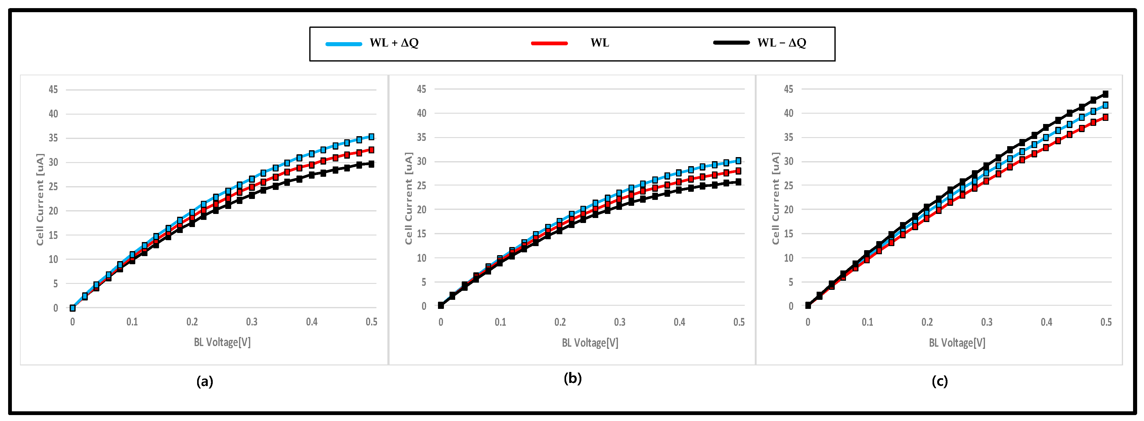
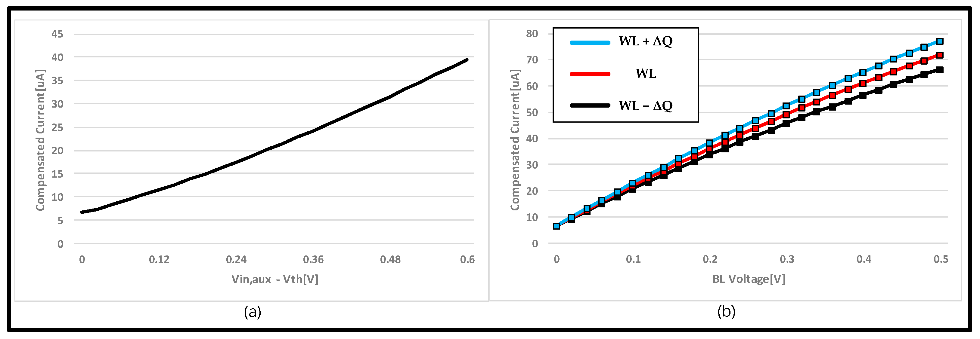
Figure 5 shows the simulation results of the drain current of the planar FG FET cells, with (3C-1T) and without (3C-1T) extended overlap capacitance (C
FDX), as a function of drain (BL) voltage. The size of C
FDX is half of C
C in this study. The drain current of the charge trap FET is also included as a reference. At first glance, the linearity is remarkably improved by C
FDX. For quantitative analysis, the cell current is fit to a polynomial,
. The regression analysis results are listed in
Table 4 using coefficients of a polynomial. As expected in Equation (4), the quadratic term is diminished by less than 25%. A reduction in the linear coefficient,
, is induced by the capacitive voltage division with the extended overlap capacitance. Curves in different colors in
Figure 5 indicate the drain current of a cell with different numbers of electrons in the floating gate or gate dielectric. Cells after electron injection (−ΔQ) and electron removal (+ΔQ) have nearly the same tendency of linearity improvement with the extended overlap capacitance.
Since the FG-drain coupling in FG FET increases the potential of the FG, the FET turns to the saturation region at a higher drain voltage as the capacitive coupling increases. The linear behavior of the drain current is extended to a wider swing range of the drain voltage. Therefore, the linearity did not deteriorate much up to a of drain voltage of 500 mV.
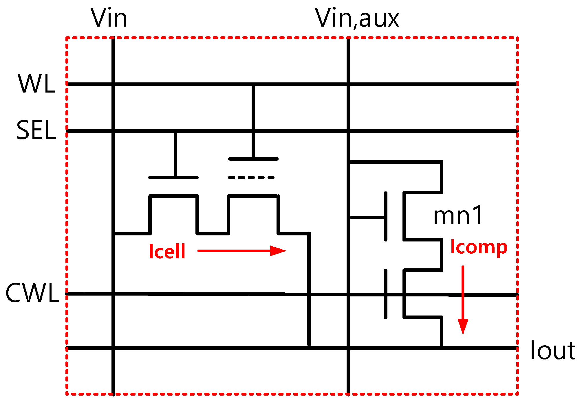
Unfortunately, current EEPROM devices transition quickly from the conventional floating gate FET to the charge trap FET. As the charges are stored in the insulating medium, such as a gate dielectric in the charge trap FET, the capacitive coupling between the drain and charge trap medium is neither considerable nor adjustable. There are no reasons to maintain the planar EEPROM structure by consuming a large area in a high density array of a neural network. Next, the area-efficient charge trap FET structure and different approaches are used to improve the linearity between the drain voltage and drain current. The following section suggests different ways of improving the linearity of the VMM cells in the charge trap FET.
4. Comparative Study
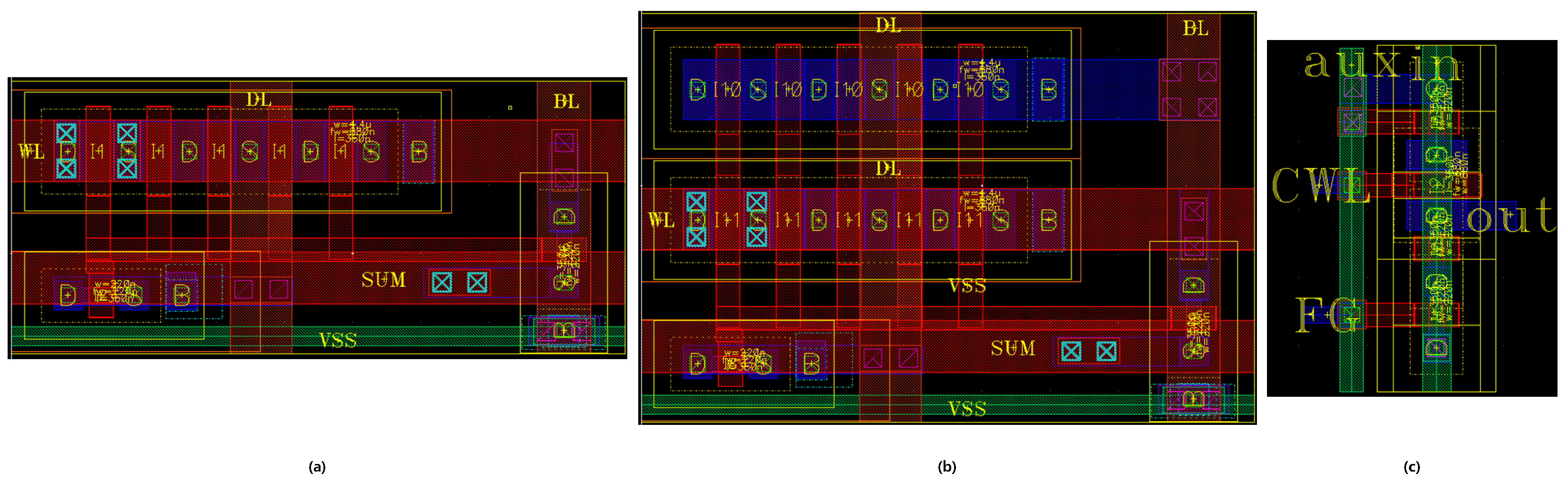
Cell layouts are compared in
Figure 10. Although the planar floating gate FETs exhibited an inherently good linearity, they occupy a very large area when compared with a group of charge trap FETs. Cells comprising 2C-1T and 3C-1T are as large as 102 F
2 and 153 F
2, respectively, where F is the minimum feature size. The charge trap FET cell with pre-distorted BL driver is as small as a EEPROM cell, which is 29 F
2. The charge trap FET with a compensation current path requires 42.6 F
2 for a cell. The size of the input drivers is not included, because the impact on the overall integrated circuit is negligibly small, as all of the cells in a column share a driver.
Table 5 compares the key performance parameters of the four VMM cells. The linearity was evaluated in three different ways. The C1/C2 ratio in the polynomial regression was used to estimate the capability for quadratic term elimination. The coefficient of determination of the linear regression was adopted to check the overall trend of straightness of the output current. The signal-to-noise ratio (SNR) and effective number of bits (ENOB) are standard metrics for linearity analysis. In the calculation of SNR and ENOB, the response of the output current of the cells after injection and removal of the trapped electrons are also included. Without considering the area penalty, the 3C-1T cell can achieve the best linearity if an unlimited size of extended coupling capacitor is available. All linearity comparisons were conducted under an input swing of 300 mV. The normalized area was defined as a figure of merit, in which the cell area was divided by the ENOB, which represents the area occupancy for 1-bit processing of the neural network. The charge trap FET cell with an auxiliary current path had the best overall performance as a VMM cell for the neural network.
5. Conclusions
After a thorough analysis of the linearity of drain current with respect to the drain voltage of the FETs, two different approaches of linearity improvement for charge storage FET cells in a neural network were identified. When a conductive floating gate node is used for charge storage, the strong coupling between the floating gate and drain node improves the linearity, because of the loose bootstrapping of the effective gate potential. The coefficient of determination for linear regression easily exceeds 99.5%, because the extended FG-drain coupling exceeds half of the FG-gate coupling. If charges are trapped in the insulating medium, such as the gate dielectric, the linearity has to be improved by any means, to add positive quadratic current. Drain voltage boosting is not recommended, because it narrows the input swing range, although boosting could improve the linearity at a small input voltage. Therefore, an additional current path with a positive quadratic current response is effective for linearity enhancement over a wide input swing range. The best linearity was achieved in a charge trap FET with an auxiliary current path, resulting in a 5.67 ENOB with 42.6 F2 cell area.


