Article

Near Field Sensing Applications with Tunable Beam Millimeter Wave Antenna Sensors in an All-in-One Chip Design

Department of Electronic Engineering, National Taipei University of Technology, Taipei 10608, Taiwan
*
Author to whom correspondence should be addressed.
Electronics 2022, 11(14), 2231; https://doi.org/10.3390/electronics11142231
Submission received: 20 June 2022 / Revised: 12 July 2022 / Accepted: 14 July 2022 / Published: 17 July 2022

Abstract

:
In this paper, a single-band beam control antenna is designed with a parallel coupler to realize a microstrip patch antenna passive wireless sensor in the form of a chip. It has a phase shift characteristic of the antenna radiation direction in the positive and negative directions. The antenna includes an orthogonal direction coupler design with a 90° parallel coupler in phase using a special structure that allows the whole chip area to be miniaturized while allowing the main beam angle to have a directivity function. The coupler is designed for the 28 GHz millimeter wave band. After feeding the patch antenna at the output port of the coupler and simultaneously feeding the excitation at the input port, the beam phase changes to +45° and +135° with a phase difference of 90°. The designed antenna size is 1160 μm × 790 μm, and the overall IC size is 1.2 mm × 1.2 mm. The power density simulation shows that the maximum power density is only 0.00797 W/kg for a 1 cm2 human sampling area, which means that the antenna sensor is suitable for use on human surfaces.

1. Introduction

With the advancement of the chip manufacturing process, the miniaturization of components has advanced to a whole new level. The antenna and millimeter wave circuits can be easily integrated into a single chip. Compared to wired sensor devices, wireless sensors have more advantages because they do not require wires to provide a transmission path, so they are easy to install and less expensive to maintain. The wireless transmission sensor can skip the setup of the sensor network, as well as expand the maximum physical limitations of the connection to the sensor. Wireless sensors are differentiated into active and passive wireless sensors. Applications of passive wireless sensors include passive radar [1,2,3,4,5], liquid sensing [6,7,8], spatial positioning [9,10,11,12,13], RFID [14,15,16,17,18,19,20,21], and blood glucose determination [22,23].
Passive wireless sensors are a core technology in many fields, such as the Internet of Things [24,25], smart cities [26], and smart healthcare [22,23,27]. Many designs in wireless sensing systems utilize a branch coupler for both outputs, which can be used to ensure that the strength of the two signals is equal [20,28,29]. With the evolution of a large number of sensors, a complex environment full of signal scattering interference has been created.
Many researchers are currently proposing microstrip patch antenna passive wireless sensors for studies such as detecting cracks on the surface of an object [30,31,32]. The resonant frequency can be clearly known under a stationary ground plane. Assuming a discontinuity in the ground plane, the resonant frequency is varied to detect cracks on the ground plane. Otherwise, the physical properties of the material can be measured by beam control. For example, in [33], the microwave frequency band was used to detect foreign material in uncleaned peanuts without shells by using the good detection effect of watery items. Compared to X-ray and infrared instruments, it has the advantage of being more cost effective. The common patch antenna is composed of two layers of metal and dielectric substrate [34], and the resonant frequency of the antenna is changed by adjusting the geometric length and width of the upper metal surface [35,36].
Beam control is the change of the main flap beam to the desired beam angle. For example, a parallel coupler makes a Beam Forming Network (BFN) designed to individually distribute the feed and phase at some degree of variation at the feed port. Alternatively, LC circuits [37], phase shifters [38,39], and phase shifters with diodes can be used to achieve beam angle switching [40,41,42,43]. The main beam can be mechanically steered using hardware devices such as motors or drivers with control software [44] to steer the radiation field pattern emitted by the guided antenna.
There are many studies investigating millimeter-wave microstrip patch antenna passive wireless sensors [45,46]. Non-contact measurement systems are suitable for liquid measurements, while millimeter wave sensors without power supply have the advantage of being maintenance-free and have a very long service life. Non-contact millimeter wave sensors are highly flexible, can measure in harsh environments, and are not easily destroyed. The signal can be easily transmitted through the fog and dust, not affected by the changing light conditions [47], and the accuracy is similar to that of laser sensors. It can also measure at high repetition rates and simultaneously measure the speed of the target at a low cost. Millimeter wave sensors that do not require power are also suitable for imaging applications, including contraband detection for flight safety and indoor space imaging because the wavelengths of radiation are long enough that they propagate through clothing, furniture, and other coverings and short enough to provide a high resolution [48].
Contact measurement systems are often used in wearable antenna sensors. Wearable antenna sensors come into contact with the human body, and the antenna is susceptible to the high dielectric constant of the human body, which changes the resonant frequency, gain, and efficiency. On the other hand, antennas can cause radiated effects on the human body. To solve both problems, researchers have changed the antenna substrate materials to allow these wearable antenna sensors to achieve better antenna gain, efficiency, lower human absorption ratio, and lower power density through material improvements and changes in antenna shape designs, such as electromagnetic band gap (EBG), artificial magnetic conductor (AMC) [49], and high impedance surface (HIS) [50].
In this paper, a microstrip patch antenna passive wireless sensor is developed on a chip. By improving the design, the coupler and the patch antenna size are successfully miniaturized. In this design, a parallel coupler is used to complete the beam control and achieve 90° phase switching. With the variation of the patch antenna, such as rectangular gap, symmetrical metal ring and PSL technology, the performance is improved and the cost is significantly reduced without increasing the usage area. In order to make the antenna sensor developed in this paper applicable to the human body surface, power density (PD) simulation is added. The simulation results are also fully compliant with FCC, ICNIRP, and IEEE specifications for PD values, which means that the designed chip is quite suitable for use in wearable devices. Compared to the branch and ring couplers, the parallel couplers can operate at any power distribution and provide a 90° phase difference [37,39]. It also allows the beam to produce a 90-degree scanning range and detects the size of the actual object by using the change of the beam close to the object, thus achieving the object scanning function. This study is to simulate the antenna characteristics using ANSYS HFSS.

2. Related Work

2.1. Subsection

Figure 1 shows the schematic diagram of the parallel coupler. Figure 2 shows the equivalent model of the parallel coupler, which contains a pair of mutual inductors, self-inductors L s and mutual inductance coupling coefficient k. Capacitance C m and C p denote the parasitic capacitance between ground and winding. The ideal parallel coupler design is for port two and port four, where port two is in phase at 0 degrees and port four is in phase at 90 degrees, and the two ports have equal phase differences of 90° in magnitude. The polarization generated by input port one or port three will achieve excellent linear polarization (LP) operation when the patch is perfectly matched at port two and port four. In addition, the ideal parallel coupler that couples to port three has very little power effect, thus producing a high level of isolation. The biggest limitation of this conventional configuration is that parallel couplers usually have only a narrow frequency band. Another technical disadvantage is that parallel couplers usually take up a large amount of space, resulting in an increase in overall size.

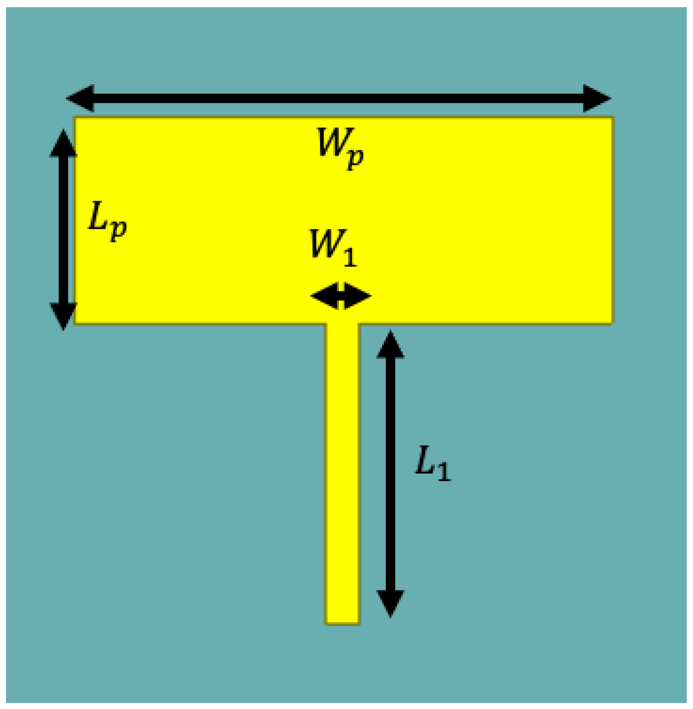
2.2. Microstrip Line Antenna Structure

A schematic diagram of a microstrip line chip antenna is shown in Figure 3. The mathematical equations for the length and width of a microstrip patch antenna are [51,52]:
W p = c 2 f r 2 ε r + 1
Δ L p = 0.712 t ( ε e f f + 0.3 ) [ w p t + 0.264 ] ( ε e f f 0.258 ) [ w p t + 0.813 ]
L p = c 2 f r ε e f f 2 Δ L p
where w p is the width of the patch antenna, L p is the length of the patch antenna, and t is the thickness of the substrate, as shown in Figure 3. Δ L p is used to describe the effect on the edge effect when the length of the antenna is adjusted such that the edge effect is decreased when the length of the antenna is reduced. ε r is the permittivity. c is the wave speed in free space. ε e f f is the equivalent permittivity.
Take the traditional PCB antenna design for example, the antenna body is designed on the surface metal layer. From the resistivity laws [53]:
R = ρ ι A
R is the resistance, ρ is the resistivity, ι is the length, and A is the cross-sectional area. When the cross-sectional area of each unit is larger, the resistance value will be smaller, and the transmission loss will also be smaller. In the design of the patch antenna, this characteristic is used to design the antenna with the main beam direction facing upward and then make the reflective surface through the back metal to enhance the antenna gain [54].

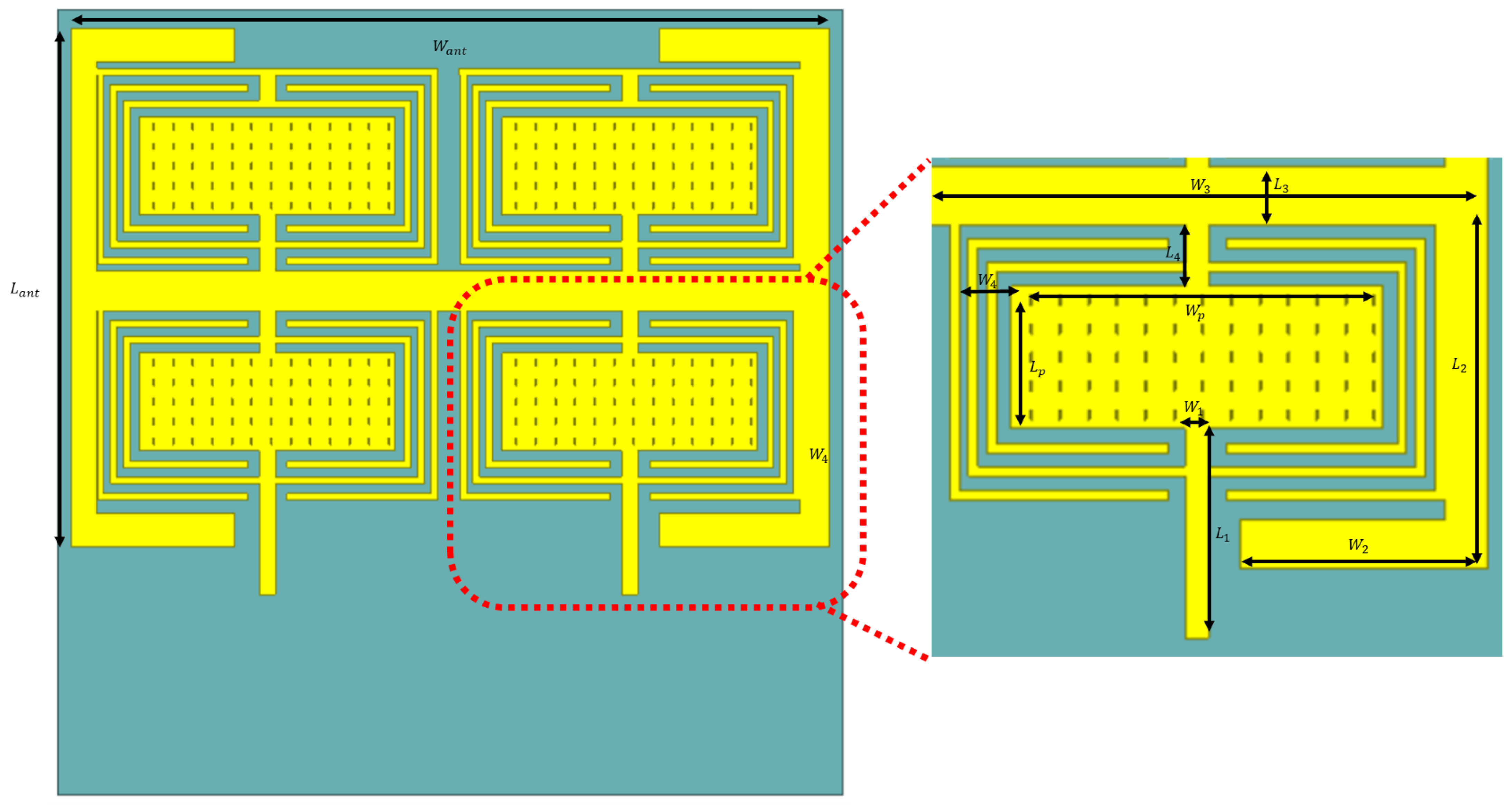
3. Chip Layout and Design

As the frequency increases, the transmission loss between the antenna and the RF circuit becomes very high. In this study, the finished product is designed for 28 GHz, which is one of the millimeter wave bands used in most countries today. The chip antenna is very helpful in reducing the transmission loss by significantly shortening the connection distance between the RF circuit and the antenna.

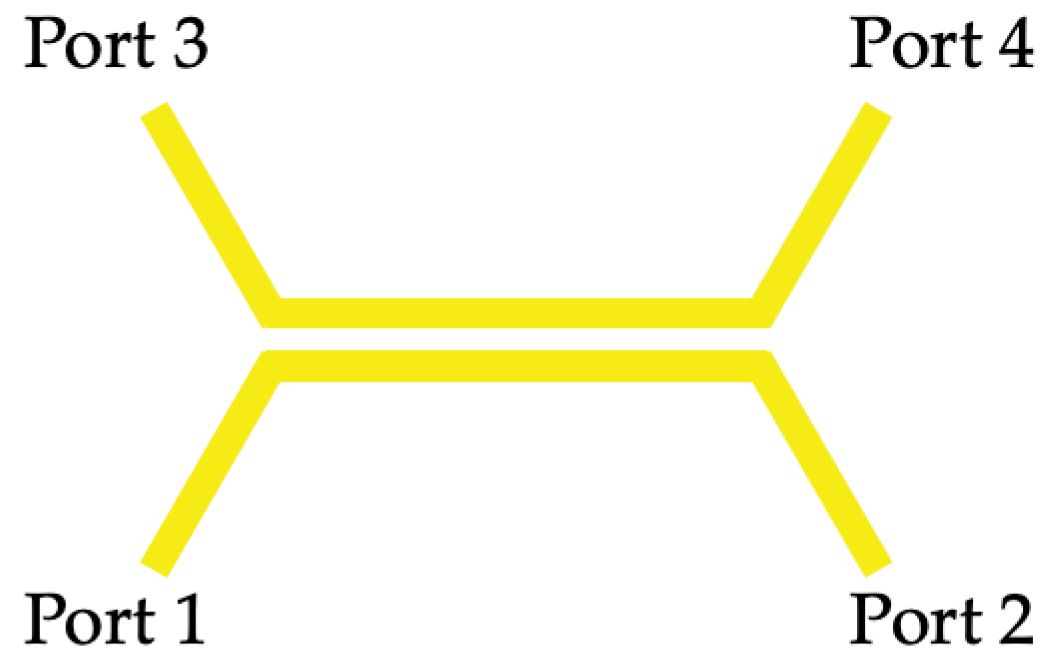
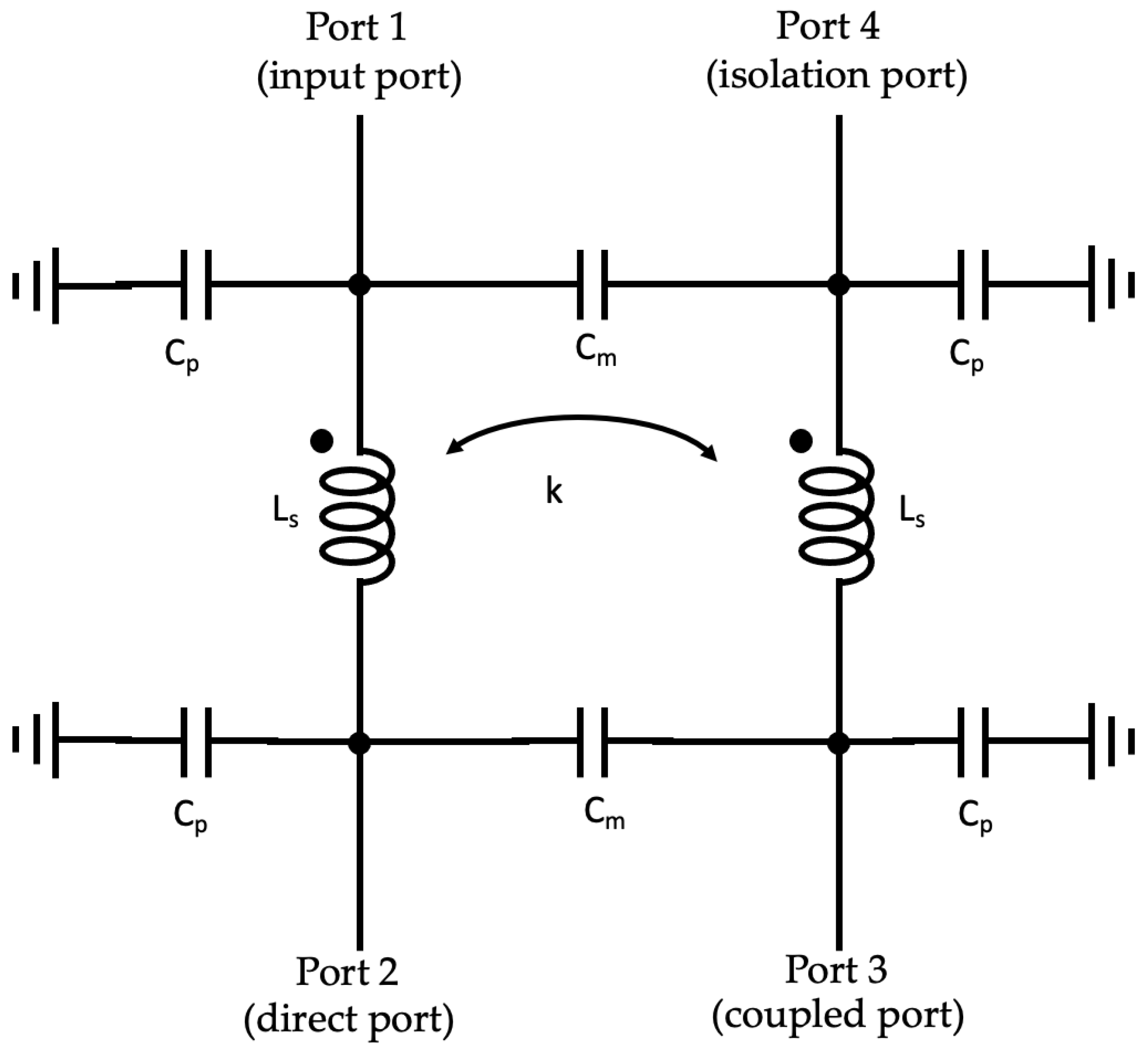
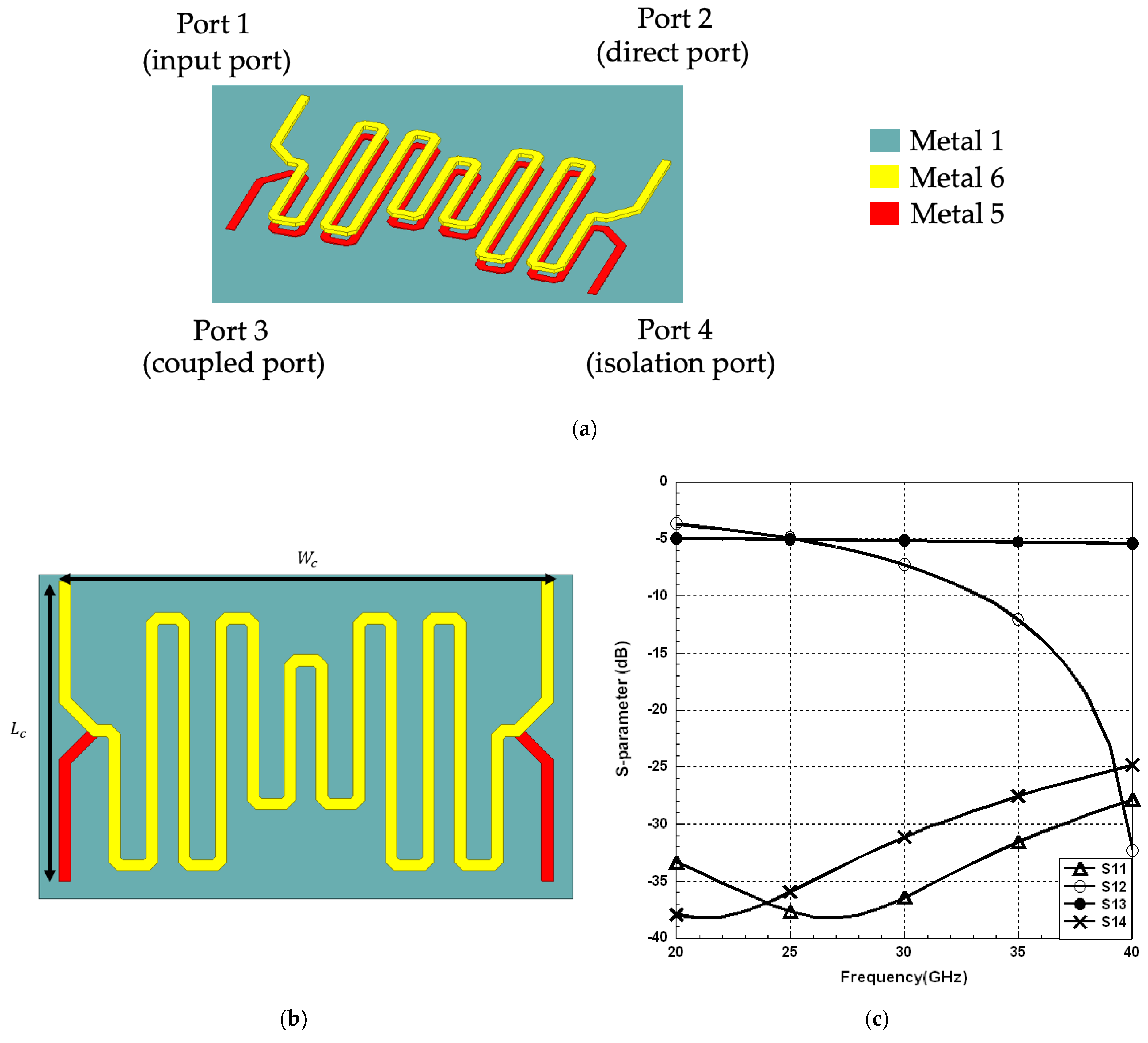
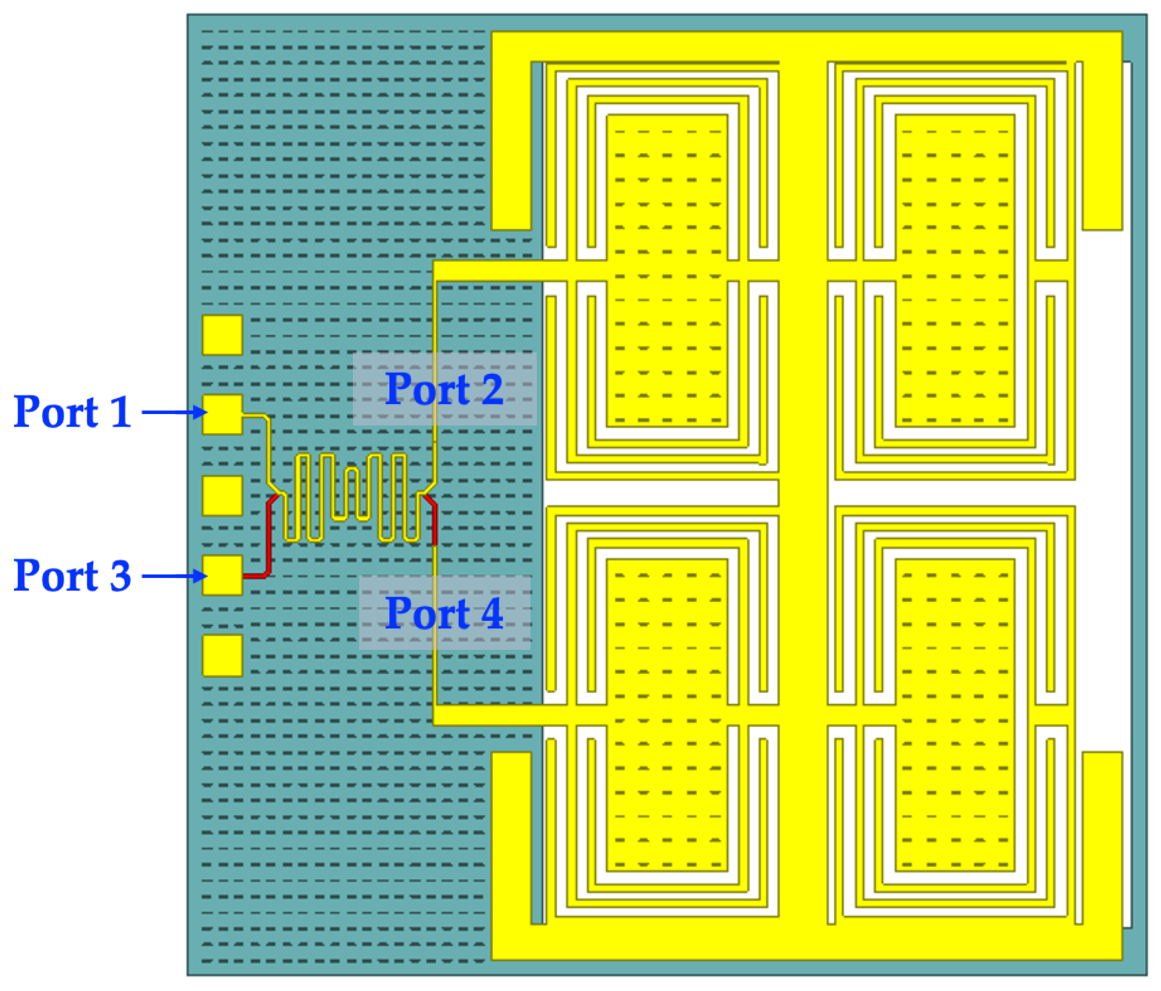
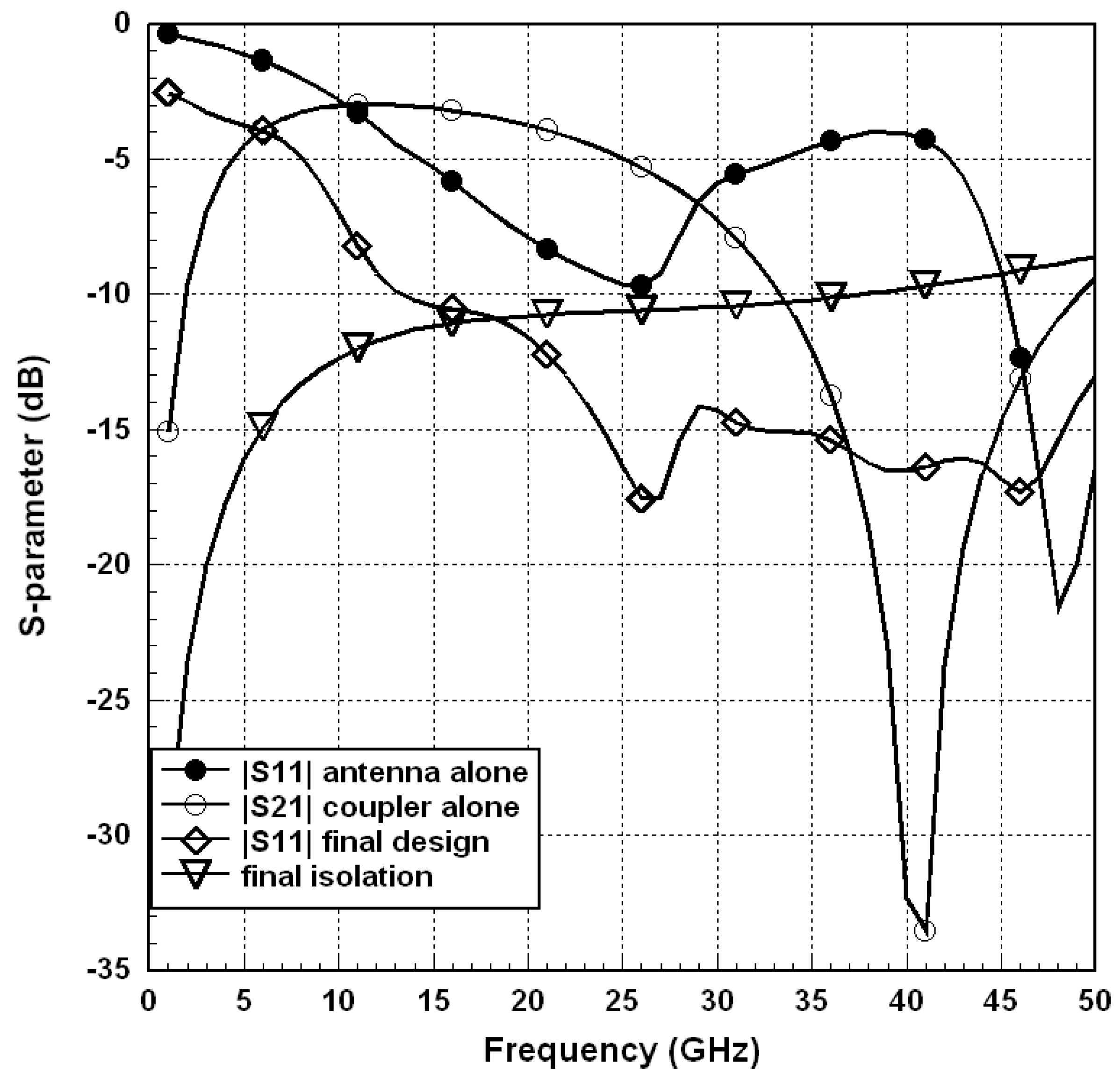
3.1. Parallel Coupler Design

The common coupler types are Parallel-line coupler, Branch-line coupler [55,56,57,58,59], Rat-race coupler [56,57,60,61,62], Lange coupler, Directional coupler [63,64,65], Lumped-Element coupler [66], and Hybrid coupler [67,68]. The design can be achieved by various structures such as Coplanar waveguide (CPW), Substrate-integrated waveguide (SIW), Microstrip line, etc. In this design, the parallel coupler structure is chosen and designed in the form of a microstrip line.
Quadrature couplers are usually designed as parallel line couplers or branch couplers [69], both of which are designed based on a quarter wavelength transmission line. However, this design is still too large for a frequency of 28 GHz.
By calculating the wavelength g through Equation (5), we can obtain the 1/4λ length at 28 GHz, which is equal to about 1.33 mm. Equation (6) is to calculate the equivalent dielectric constant ε e f f , ε r is the dielectric constant, H is the substrate thickness, W is the microstrip line width, and T is the aluminum thickness [52].
λ g = 300 f G H z ε e f f
ε e f f = ε r + 1 2 + ε r 1 2 { 1 1 + 12 ( H W ) + 0.04 [ 1 ( W H ) 2 ] }
The standard CMOS implementation of a parallel coupler is achieved using a CMOS multi-metal layer structure with a wide-sided coupling. Figure 4 shows an example layout where the parallel coupler is placed between the top and second layers to increase the coupling amount by direct stacking. The first winding layout starting from port 1 is on the thinner metal 6 layer with a thickness of 2.34 μm and then along the metal 6 layer to port 2. Meanwhile, the second winding is placed on the metal 5 layer starting from port 3 with a thickness of 0.53 μm and then completely overlaps with the metal 6 winding. The grounding layer below the stacked windings is removed to obtain a high k value. By this improvement in architecture, about 50% of the usable area can be saved [69].

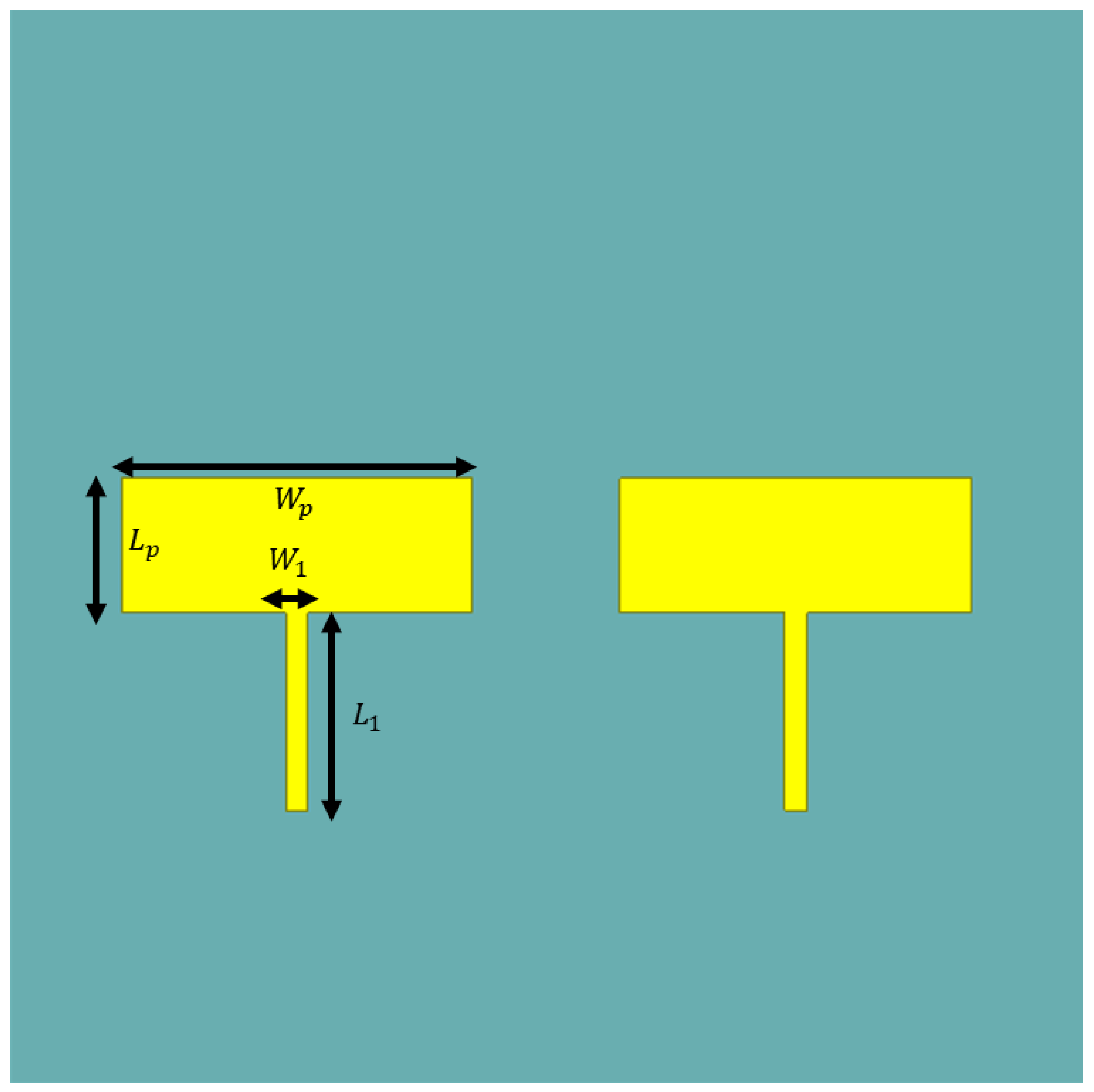
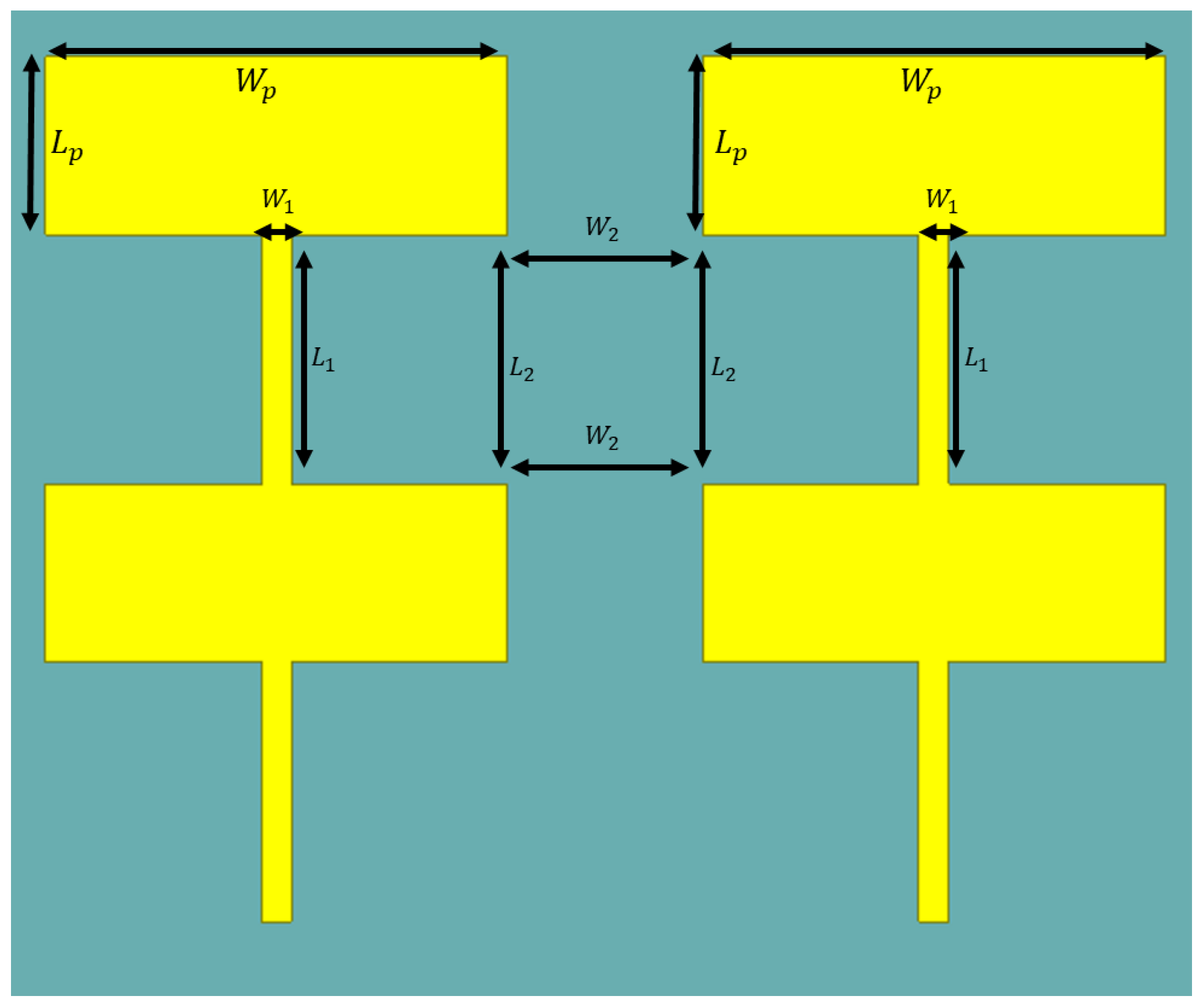
3.2. Structure of Microstrip Line Chip Antenna

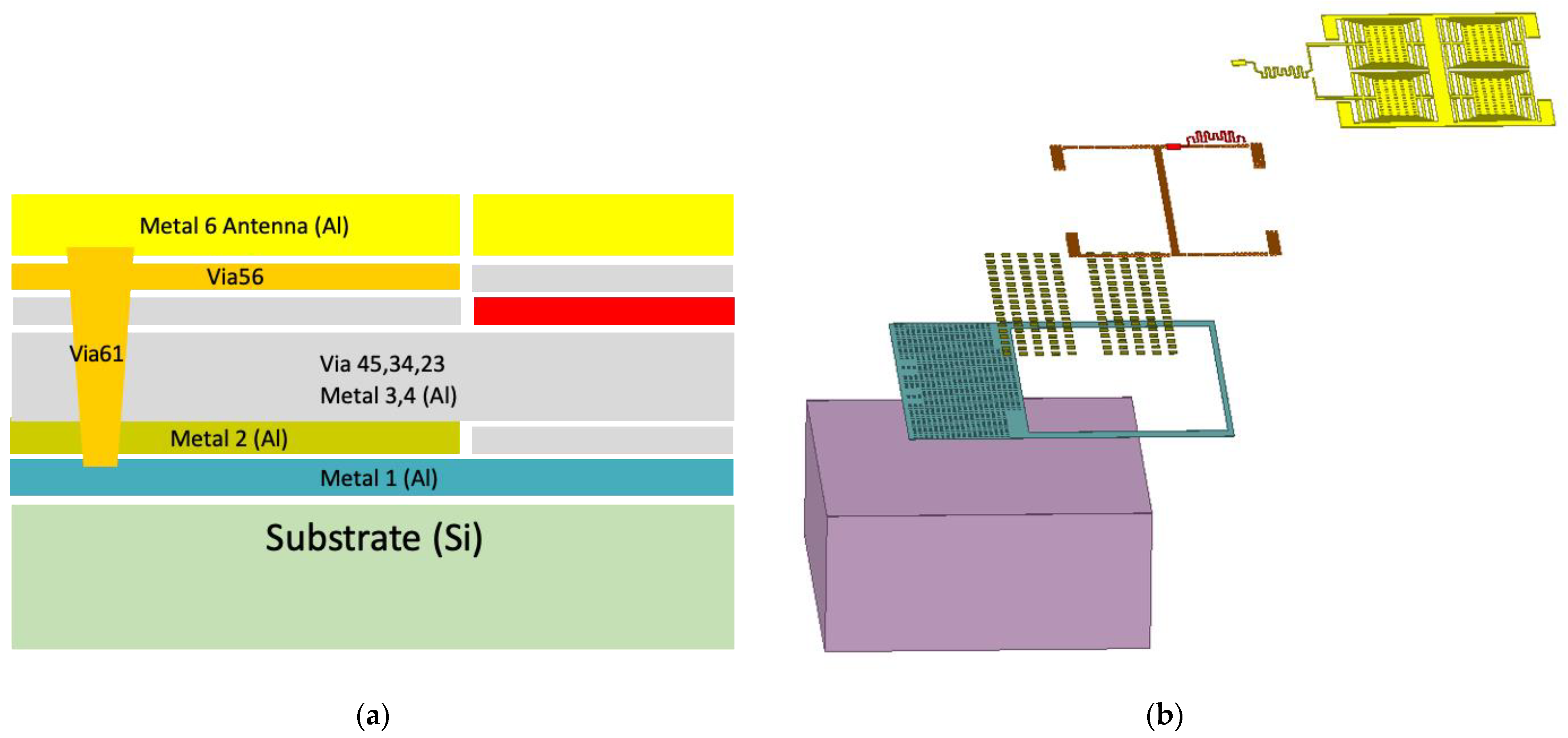
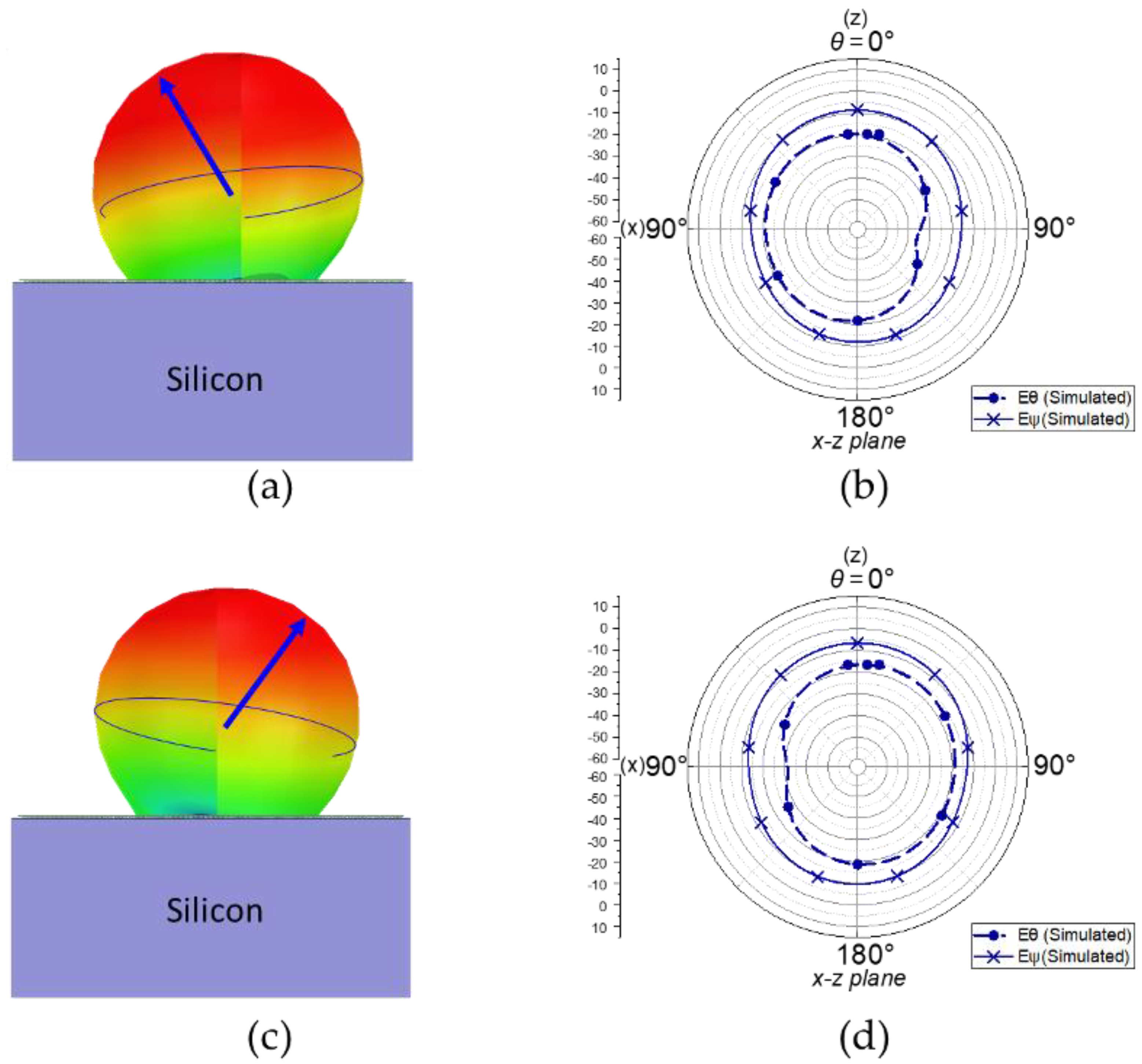
3.2.1. Antenna Stacking Design

As shown in Figure 4, the parallel coupler designed in this paper has four ports, so two sets of antennas of Figure 3 are needed to form a symmetrical antenna structure as in Figure 5. The antenna dimensions are L P = 150   μ m , W P = 90   μ m , L 1 = 210   μ m , and W 1 = 25   μ m . In order to improve the antenna gain, two antenna structures of Figure 5 are formed as Figure 6, where L 2 = 210   μ m and W 2 = 164.5   μ m . Figure 7 shows the simulated antenna gain for both Figure 5 and Figure 6 in antenna structures. The diamond-shaped curve “antenna” in Figure 7 is the antenna gain of Figure 5. The “x” curve in Figure 7, “Series antenna”, is the antenna gain for Figure 6. So, Figure 7 clearly shows that the antenna structure of Figure 6 is indeed able to increase the gain.

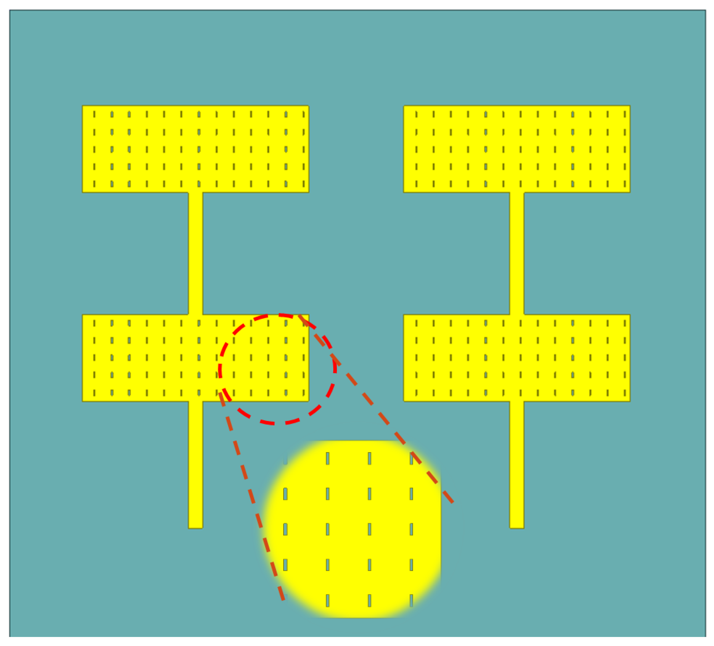
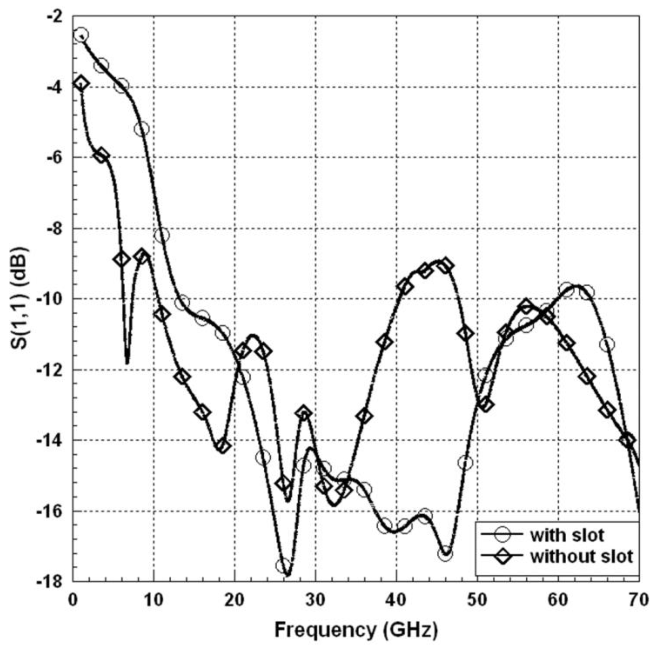
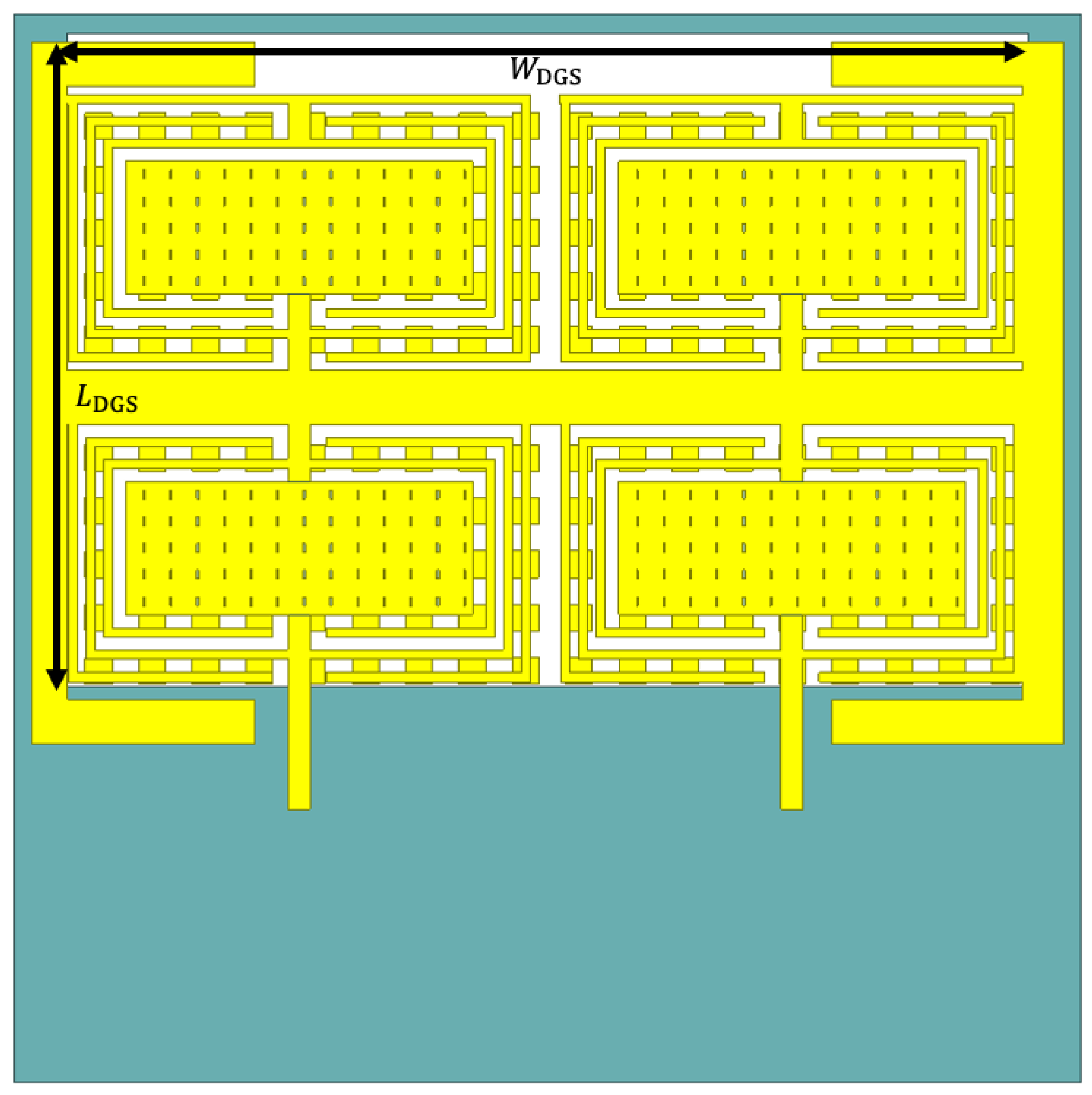
3.2.2. Rectangular Slot

To improve the performance of the chip, a chip antenna with a rectangular slot is proposed in this study, as shown in Figure 8. As shown in Figure 9, the available bandwidth is narrower without the rectangular slot, and the standard S 11 < 10   dB can produce a bandwidth of 12–60 GHz.

3.2.3. Gain Enhancement

In [70], asymmetric square metal rings are described for achieving Gain Enhancement to improve the overall gain. By using this concept, the square metal ring design is added to the antenna of Figure 8 and makes it symmetrical, as shown in Figure 10. Figure 11 and Figure 12 show the simulated field pattern without and with the addition of symmetric square metal rings, respectively. Figure 11a–c shows the x-y, x-z, and y-z planar field patterns when port 1 is fed in, and Figure 11d–f shows the x-y, x-z, and y-z planar field pattern when port 3 is fed in. Figure 12a–c shows the x-y, x-z, and y-z planar field pattern when port 1 is fed in, and Figure 12d–f shows the x-y, x-z, and y-z planar fields when port 3 is fed in. Comparing Figure 11 and Figure 12, the beam can be guided to the correct direction when a symmetric square metal ring is added.

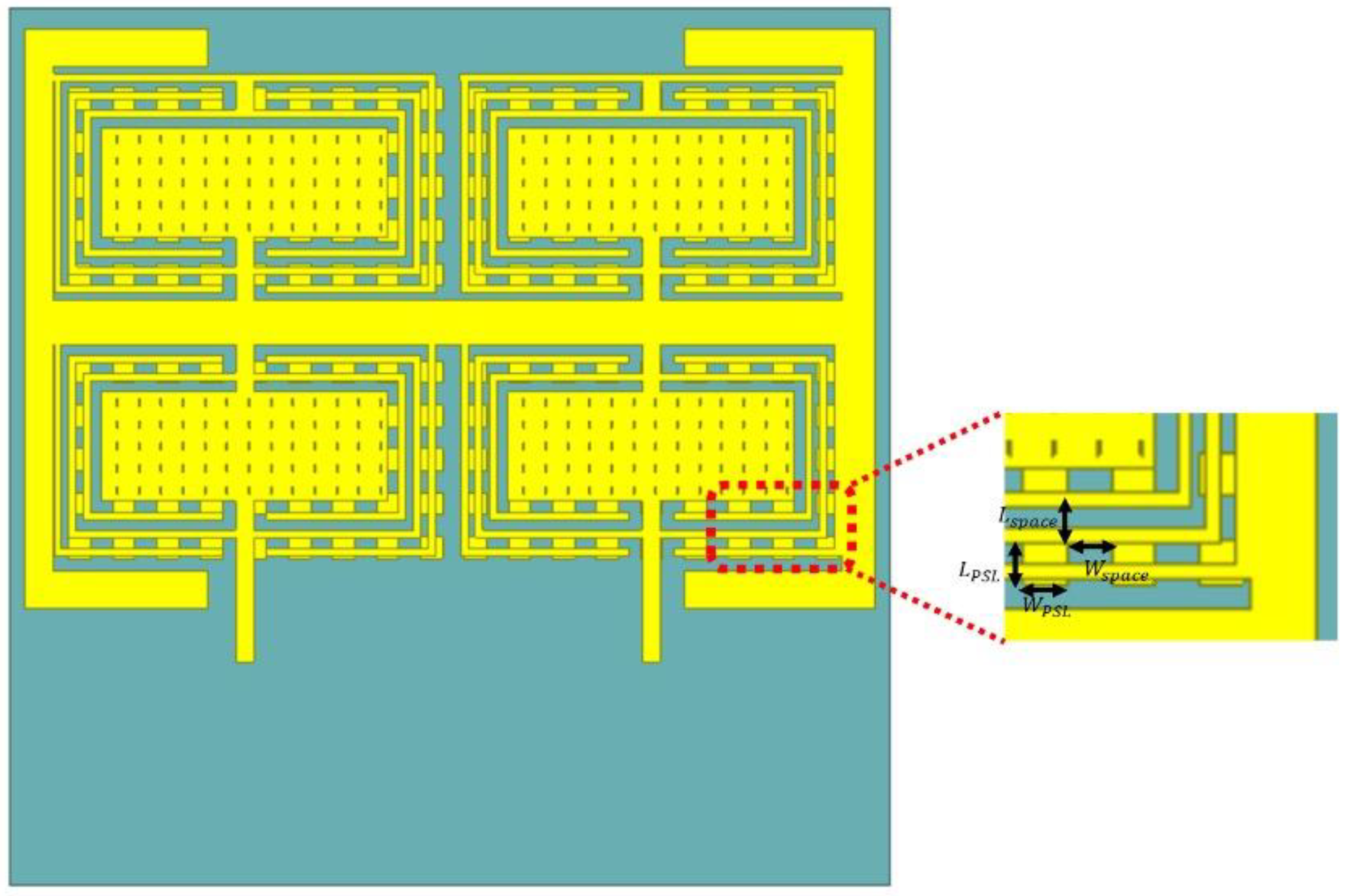
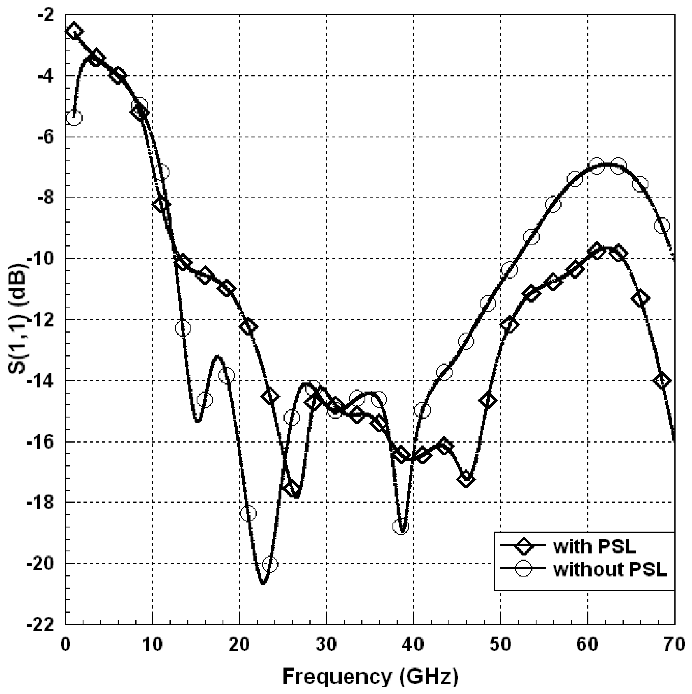
3.2.4. Partially Shield Layer

In order to further enhance the antenna gain, the PSL (partially shield layer) technique is added [71], as in Figure 13. Metal PSL is first added to metal layer 2, and then the bottom metal layer, metal 1, is hollowed out in a symmetrical manner for the defective ground structure (DGS), as in Figure 14. An additional capacitive element is created between the top metal and PSL layers to effectively converge the resonant frequencies, resulting in a smaller antenna size and improved gain. As shown in Figure 15, a bandwidth of 12~60 GHz can be generated at S 11 < 10   dB .
From Equation (7), the parallel plate capacitor formed by two metal layers filled with oxide has a larger capacitance, allowing the center frequency of the antenna to be effectively reduced. As the thickness of the oxide increases, the effective capacitance decreases, the frequency shifts to higher frequencies again, and the input reflection impedance is better [71].
f r 1 C e q
where f r is the resonant frequency. C e q is the value of the capacitance between the metal layers, that is, the equivalent capacitance between the top metal and the PSL.

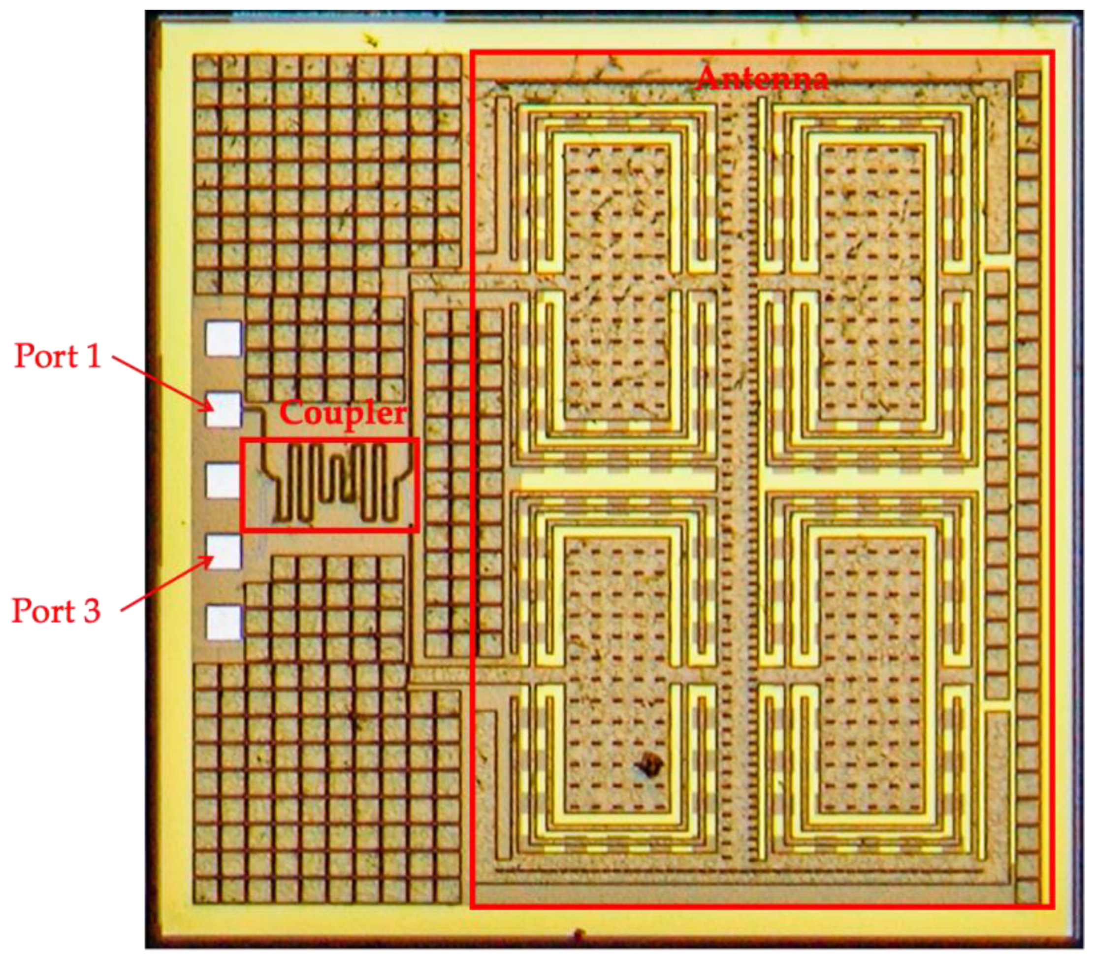
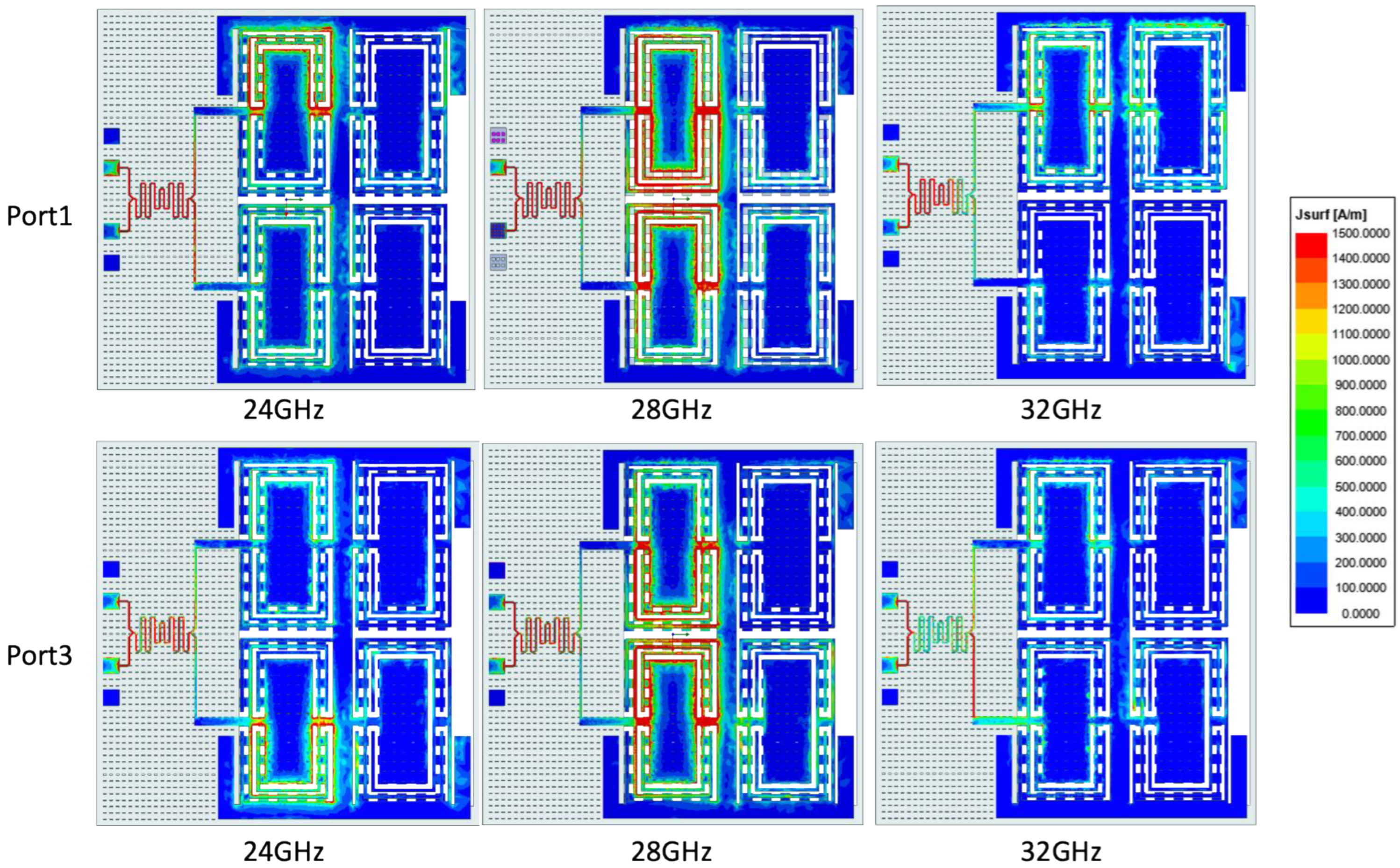
3.3. Proposed IC Design

In this paper, we propose a solution as shown in Figure 16, combining the structure of Figure 4 and Figure 14. In this particular design, the antenna is patterned on a 600-micron-thick silicon substrate using 2.34-micron aluminum as the conductor. The designed antenna size is 1160 μm × 790 μm. One of the keys to successfully designing a chip on a silicon semiconductor chip is to comply with metal density design rules. Even at millimeter wave frequencies, the antenna can be small enough to fit on the chip, but it is still the largest component on the chip. Figure 17a shows the proposed antenna in the TSMC 0.18 μm CMOS process using the metal layers, which shows that the lowest layer of the substrate is made of silicon, and metals 1–6 are made of aluminum. The layers used in this design are metal 1, metal 2, metal 5, and metal 6. The thicknesses of each layer are 0.53 μm for metal 1 and 5 and 2.34 μm for metal 6. The antenna and coupler are designed using metal 6.
Figure 17b shows the structure of each metal layer stacked in an exploded view, which contributes to the miniaturization of the antenna area, unlike conventional microwave designs [1,72,73,74]. For antenna measurements, two inputs, port 1 and port 3, are excited with probes. No additional circuitry is required for the ground. Finally, in order to provide more freedom in optimizing the antenna characteristics, a trade-off was made in the overall antenna size, and a metal frame was used to wrap the antenna.
The distance between antennas is calculated as a multiple of λ/4 of 28 GHz. Equation (8) shows that E is the electrical length, L is the physical length, and c is the speed of light [75]. By calculation, the electrical length from port 1 of the parallel coupler input to port 2 of the antenna feed is 1335 μm, which is calculated using the application frequency band in this paper.
E = L f ε e f f c
The port 1 to port 2 analog phase angle is −90 degrees, the port 1 to port 4 phase is −180 degrees, and the phase difference is −90 degrees, forming two parallel stacked couplers. In the signal conversion process, the input port 1 and port 2 will pass through the upper and lower bending parallel couplers, respectively. The simulation result of Figure 18 shows that after combining the coupler with the antenna, the standard S 11 < 10   dB produces a bandwidth of 12~60 GHz. The port isolation is −6.5 dB.
Figure 19a–d shows the simulated 3D and 2D planar field patterns of the coupler antenna resonant frequency at 28 GHz, and it can be seen that the proposed coupler can actually achieve the beam control effect. The Eθ beam angles of +45° and +135° can be seen in the x-z plane for each of the port 1 and port 3 feeds of Figure 16, with an angular difference of 90°. From the x-z plane field pattern section of Figure 19a,b, it can be observed that port 1 feeds in with a beam direction of +135°. The x-z plane field pattern section in Figure 19c,d shows that port 3 feeds in with a beam direction of +45°. When the coupler antenna feeds into the excitation of port 1 and port 3, it produces different phase radiation directions with an angular difference of 90° between them.

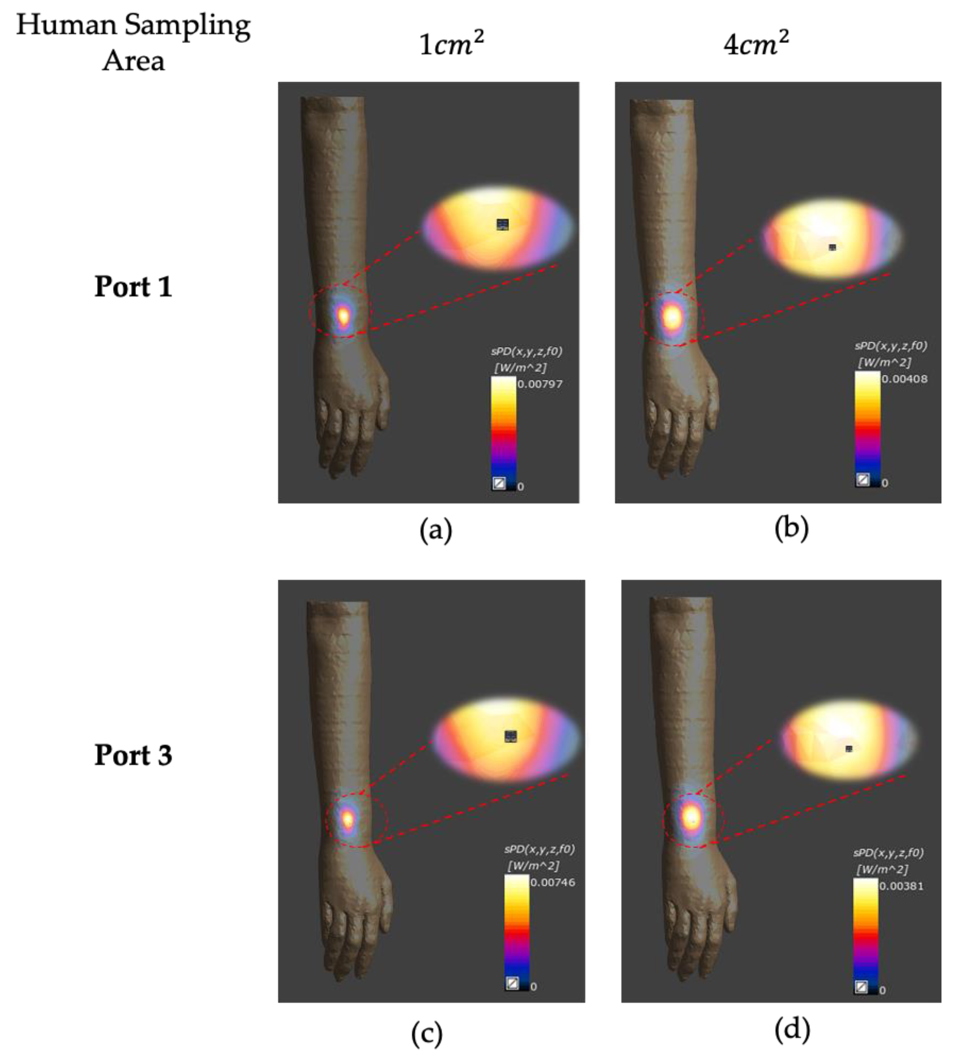
4. Power Density Simulation

The design takes into consideration the development of wearable devices, and the design of the microstrip patch antenna utilizes a different structure to generate radiation from the antenna. The power density is calculated by reflecting back to the antenna surface from the ground, which generates most of the radiation, and only a small portion of the radiation power is lost through the ground. When the antenna is operated in a human environment, the human body absorbs the radiated energy from the lost electromagnetic waves. The long-term exposure or short-term absorption of high radiation levels can have negative health effects. To ensure public safety, the Federal Communications Commission (FCC) established the electromagnetic field (EMF) standard in 1996, and the FCC limits the public exposure specific absorption rate (SAR) of mobile devices to 1.6 W/kg. In high frequency states, the wavelength is very short, so the SAR is ignored in favor of power density. However, the wavelength is very short at a high frequency, so the SAR is ignored and the power density (PD) is calculated instead [58]. At frequencies above 10 GHz, EM waves may be absorbed by the human surface, resulting in an increase in temperature. This problem can be investigated by PD simulations, and Table 1 shows the specifications of the Federal Communications Commission (FCC), ICNIRP, and IEEE for PD values [76].
The PD safety limit is 10 W/ m 2 . The equation is as follows [77].
S i n c m ( A , d , β χ ) = 1 A A | Re [ E ( d , β χ ) × H * ( d , β χ ) ] | d s x
Figure 20 shows the input power of the antenna feed point at 0.1 W (20 dBm) and a frequency of 28 GHz to calculate the PD value.
When wearable devices support frequency bands above 6 GHz, power density (PD) measurements are required by FCC regulatory testing requirements. This paper uses Sim4Life to perform PD simulations. Figure 21 shows the power density simulation results when the signal is fed to the chip antenna. The input power from the feed point is 0.1 W (20 dBm) when the antenna is 10 mm away from the arm. Figure 20a,b shows the PD results of 1 cm 2 and 4 cm 2 sampling area when the wafer is fed from port 1. The PD results are shown in Figure 20c,d for the sampling area of 1 cm 2 and 4 cm 2 when the chip is fed from port 3. Simulation results show that the chip antenna has a maximum PD of 0.00797 W/ m 2 at 28 GHz for a human sampling area of 1 cm 2 and 0.00381 W/ m 2 at 4 cm 2 , which is well below the certification limit of 10 W/ m 2 .

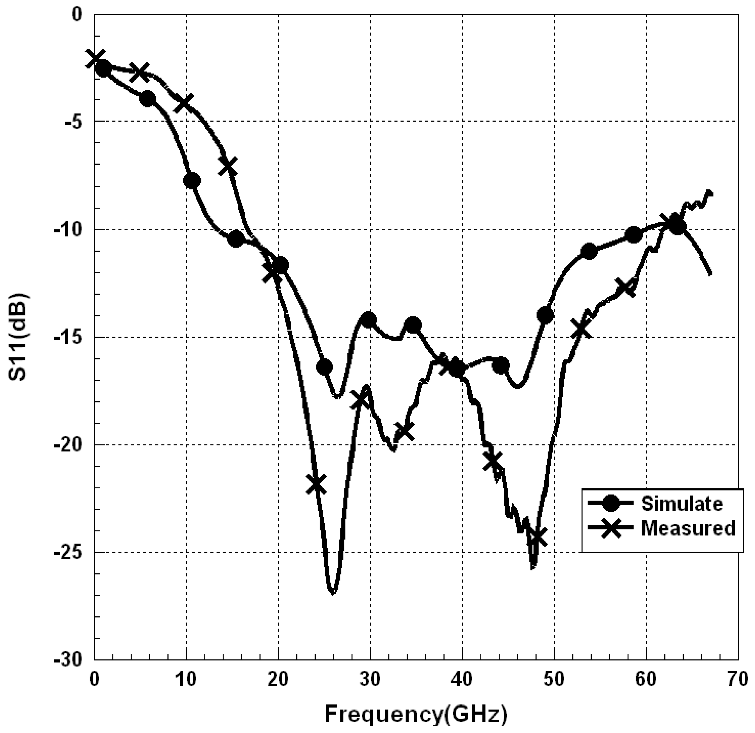
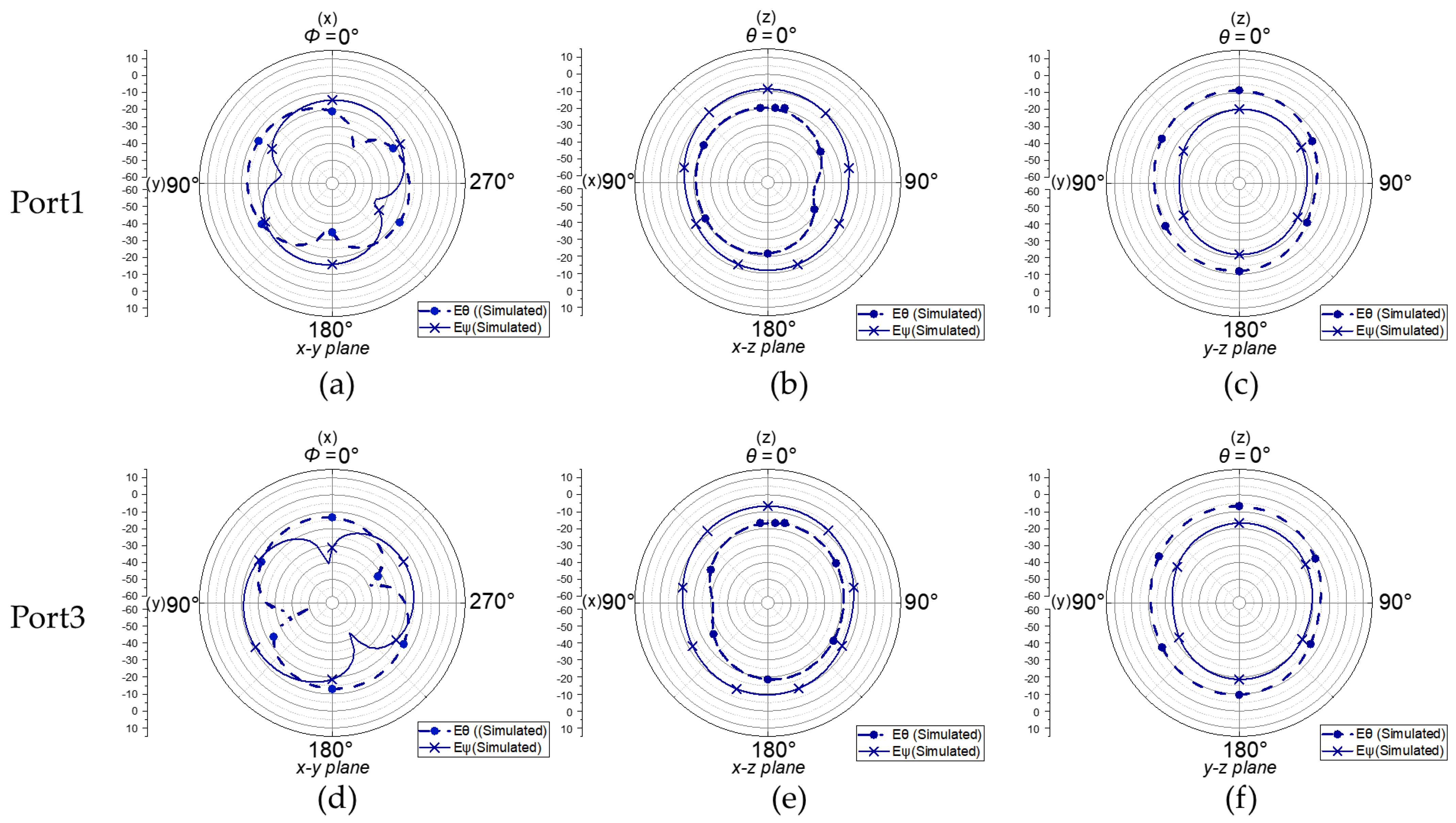
5. Experimental Setup and Results

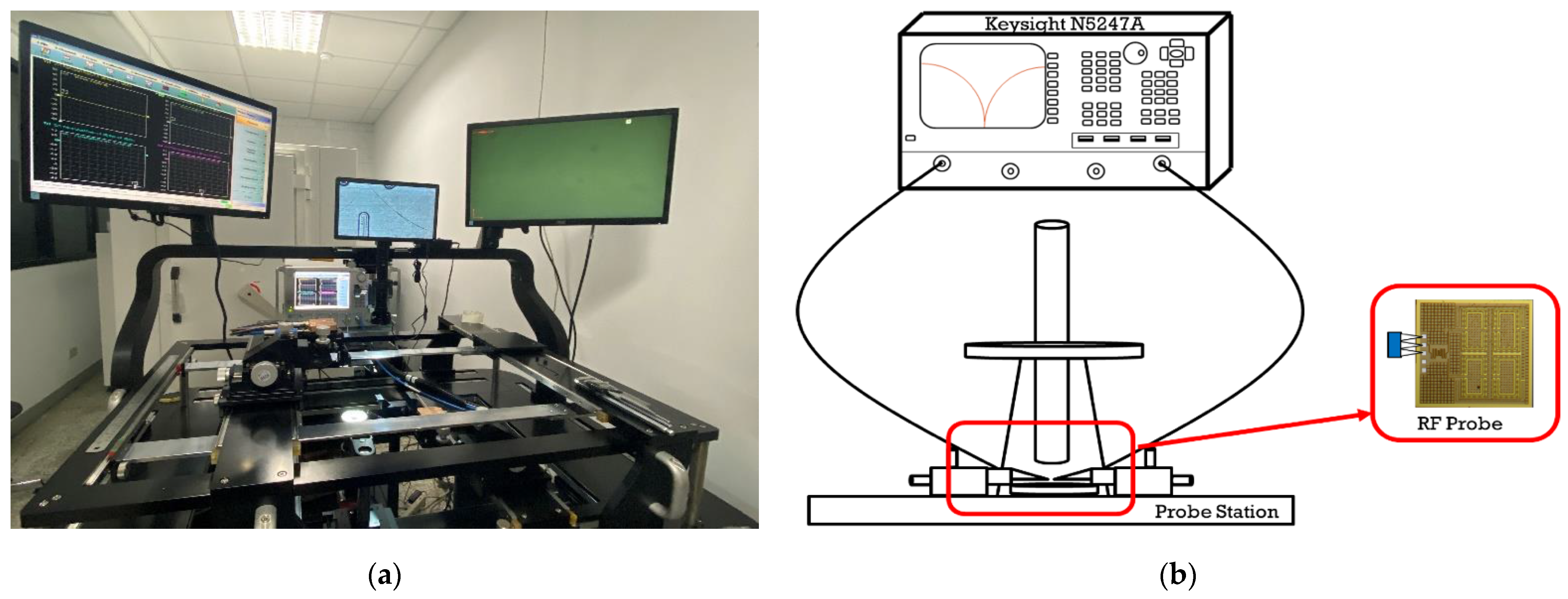
5.1. Measurement System

The measurement system used in this study is shown in Figure 21a. The network analyzer used is Keysight N5247A PNA X Network Analyze, and the probe station is FAST AND BEST CO. The measurement range is from 10 MHz to 67 GHz, and Figure 21b shows the measurement schematic.

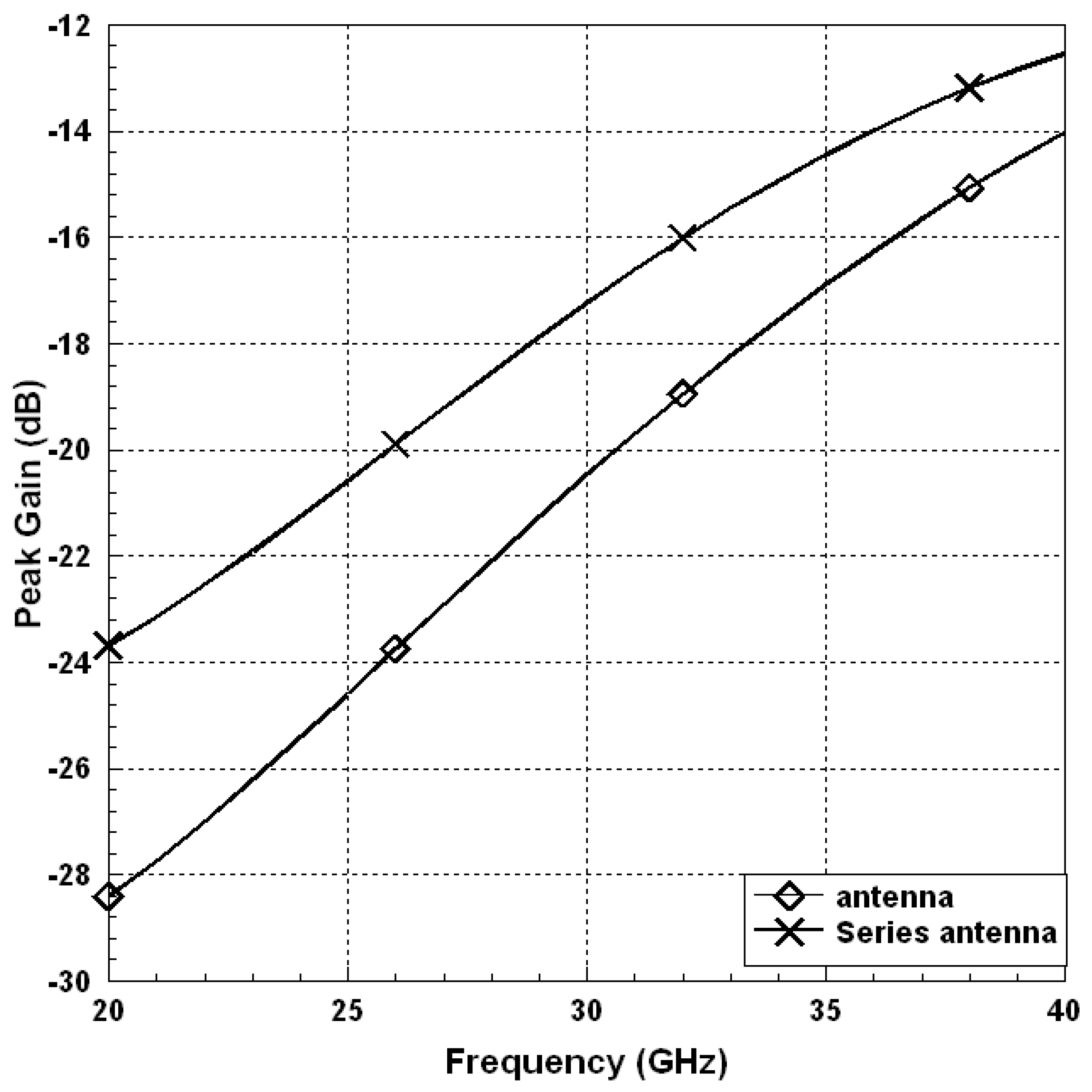
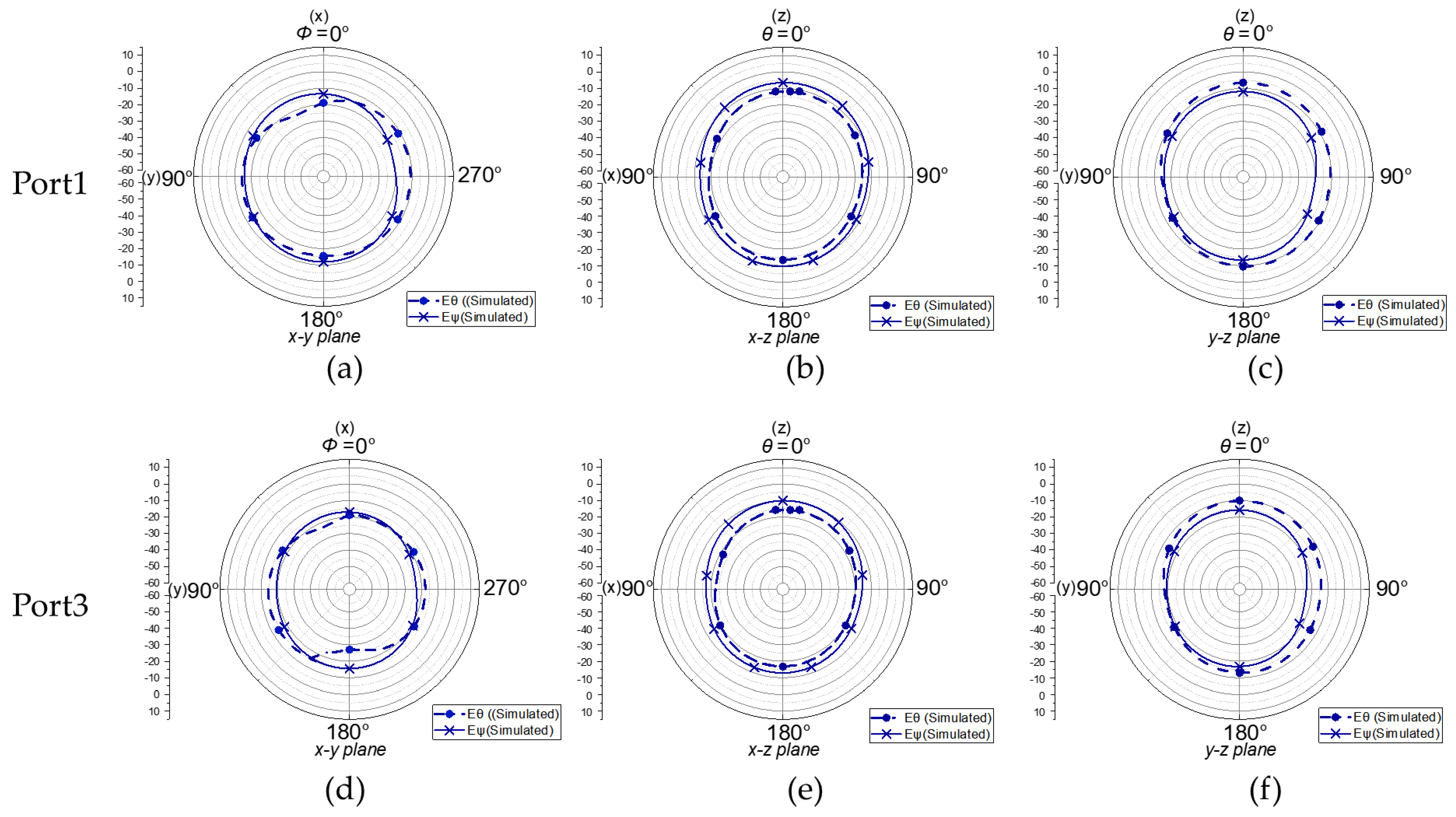
5.2. Measurement Results

The physical chip antenna is shown in Figure 22, and the size is 1.2 mm × 1.2 mm. When port 1 is excited, the antenna radiates a linearly polarized wave in the broadside direction. If port 3 is excited, the same phenomenon will occur as for port 1. Because the design of this paper is symmetric, the antennas operating at both ports should have very similar return losses. Therefore, in this article, only the far-field measurements using Port 1 excitation are shown.
Figure 23 shows the simulated and measured S-parameters. At −10 dB, the antenna measured an |S11| operating bandwidth of 115% (16.7–61.9 GHz). At −15 dB, the |S11| operating bandwidth is 84.7% (21.3–52.6 GHz). At −20 dB, it is 17.8% (23.55–28.11 GHz) and 14.71% (42.86–49.64 GHz), respectively. The antenna will be highly efficient since it is designed without the use of active components such as diodes or transistors, and the actual S11 measurements compare favorably with the simulated results.
Figure 24 shows the proposed antennas fed from port 1 and port 3, respectively. Observe the surface current distribution at 24 GHz, 28 GHz, and 32 GHz frequency points. When the frequency points are at 24 GHz and 32 GHz, the surface current distribution is not uniform and the surface current strength is weak, so the correct beam angle cannot be generated. In 28 GHz, the metal ring structure near the feedthrough has a stronger symmetrical resonant current compared to 24 GHz and 32 GHz, which produces the correct beam angle.
Table 2 shows the performance of the proposed coupler antenna compared to other coupler antennas of different architectures in the 28–30 GHZ band. The comparison includes the available bandwidth, size, and dimensions. It is clear that the proposed coupler antenna has a significant size advantage compared to other 28 GHz antennas.

6. Conclusions

In conventional beam control designs, an extremely large structure is often used. This paper introduces a beam-switching chip patch antenna sensor with a wide available frequency band and excellent isolation characteristics. First the chip is designed as a square patch antenna in the form of a microstrip line, which is excited in a parallel manner by a parallel coupler. By using the coupler, the desired beam direction can be adjusted by feeding the appropriate input endpoints. Finally, the results are verified by a real experiment and show a good agreement between measurement and simulation. It has a wide operating band of 84.7% (21.3–52.6 GHz) at S-parameter standards below −15 dB. Within this band, an isolation of more than 15 dB is achieved. In this design, the cost can be significantly reduced, the space used can be decreased, and the same effect can be achieved. Finally, the simulation was performed for power density. The simulated results show that it not only passes the FCC, ICNIRP, and IEEE standards but also is much lower than the standard and has very low damage to the human body, which is very suitable for wearable devices. Therefore, an antenna sensor can be applied to the surface of the human body for body measurement in the future, such as Blood Glucose Monitoring.

Author Contributions

Conceptualization, M.-A.C.; methodology, M.-A.C.; software, M.-A.C. and W.-J.L.; validation, M.-A.C., W.-J.L. and C.-W.L.; formal analysis, M.-A.C., W.-J.L. and C.-W.L.; investigation, C.-W.L., and W.-J.L.; resources, M.-A.C.; writing-original draft preparation, M.-A.C. and C.-W.L.; writing-review and editing, M.-A.C.; visualization, M.-A.C.; supervision, M.-A.C.; project administration, M.-A.C.; funding acquisition, M.-A.C. All authors have read and agreed to the published version of the manuscript.

Funding

This research received no external funding.

Institutional Review Board Statement

Not applicable.

Informed Consent Statement

Not applicable.

Data Availability Statement

All data are included within manuscript.

Conflicts of Interest

The authors declare no conflict of interest.

References

  1. Paquit, M.; Arapan, L.; Feng, W.; Friedt, J.-M. Long range passive RADAR interrogation of subsurface acoustic passive wireless sensors using terrestrial television signals. IEEE Sens. J. 2020, 20, 7156–7160. [Google Scholar] [CrossRef]
  2. Hallil, H.; Dejous, C.; Hage-Ali, S.; Elmazria, O.; Rossignol, J.; Stuerga, D.; Talbi, A.; Mazzamurro, A.; Joubert, P.-Y.; Lefeuvre, E. Passive resonant sensors: Trends and future prospects. IEEE Sens. J. 2021, 21, 12618–12632. [Google Scholar] [CrossRef]
  3. Gomez-del-Hoyo, P.; del-Rey-Maestre, N.; Jarabo-Amores, M.-P.; Mata-Moya, D.; Benito-Ortiz, M.-d.-C. Improved 2D Ground Target Tracking in GPS-Based Passive Radar Scenarios. Sensors 2022, 22, 1724. [Google Scholar] [CrossRef]
  4. Speirs, P.J.; Ummenhofer, M.; Schüpbach, C.; Renker, M.; Wellig, P.; Cristallini, D.; O’Hagan, D.W.; Kohler, M.; Murk, A. Comparison of DVB-T Passive Radar Simulated and Measured Bistatic RCS Values for a Pilatus PC-12 Aircraft. Sensors 2022, 22, 2766. [Google Scholar] [CrossRef]
  5. Knioła, M.; Rogala, T.; Szczepaniak, Z. Counter-Passive Coherent Locator (C-PCL)—A Method of Remote Detection of Passive Radars for Electronic Warfare Systems. Electronics 2021, 10, 1625. [Google Scholar] [CrossRef]
  6. Prasanna, R.; Annaram, K.; Shanker, N. Multilayer Flexible Substrate Antenna Sensor for PT Measurement From Blood Plasma to Avoid Turbidity and Reagent Sensitivity Variations Through Regression Modelling. IEEE Sens. J. 2021, 21, 10409–10419. [Google Scholar] [CrossRef]
  7. Tajin, M.A.S.; Mongan, W.M.; Dandekar, K.R. Passive RFID-based diaper moisture sensor. IEEE Sens. J. 2020, 21, 1665–1674. [Google Scholar] [CrossRef]
  8. Rivera-Lavado, A.; García-Lampérez, A.; Jara-Galán, M.-E.; Gallo-Valverde, E.; Sanz, P.; Segovia-Vargas, D. Low-Cost Electromagnetic Split-Ring Resonator Sensor System for the Petroleum Industry. Sensors 2022, 22, 3345. [Google Scholar] [CrossRef]
  9. Dash, L.; Pattanayak, B.K.; Mishra, S.K.; Sahoo, K.S.; Jhanjhi, N.Z.; Baz, M.; Masud, M. A Data Aggregation Approach Exploiting Spatial and Temporal Correlation among Sensor Data in Wireless Sensor Networks. Electronics 2022, 11, 989. [Google Scholar] [CrossRef]
  10. Yu, Z.; Fu, Y. A Passive Location Method Based on Virtual Time Reversal of Cross Antenna Sensor Array and Tikhonov Regularized TLS. IEEE Sens. J. 2021, 21, 21931–21940. [Google Scholar] [CrossRef]
  11. Storrer, L.; Yildirim, H.C.; Crauwels, M.; Copa, E.I.P.; Pollin, S.; Louveaux, J.; De Doncker, P.; Horlin, F. Indoor tracking of multiple individuals with an 802.11 ax Wi-Fi-based multi-antenna passive radar. IEEE Sens. J. 2021, 21, 20462–20474. [Google Scholar] [CrossRef]
  12. Al-Jarrah, M.A.; Al-Dweik, A.; Ali, N.T.; Alsusa, E. Joint estimation of location and orientation in wireless sensor networks using directional antennas. IEEE Sens. J. 2020, 20, 14347–14359. [Google Scholar] [CrossRef]
  13. Suchodolski, T. Active Control Loop of the BOROWIEC SLR Space Debris Tracking System. Sensors 2022, 22, 2231. [Google Scholar] [CrossRef]
  14. Jouali, R.; Aoutoul, M.; Ouahmane, H.; Ahmad, S.; Had, A.; El Moukhtafi, F.; Parchin, N.O.; See, C.H.; Abd-Alhameed, R. Design of an Analog RFID-Based Tag Antenna with Opened Circuited L-Shaped Stubs for Applications in Localization. Electronics 2022, 11, 1027. [Google Scholar] [CrossRef]
  15. Tao, Y.; Wu, L.; Sidén, J.; Wang, G. Monte Carlo-Based Indoor RFID Positioning with Dual-Antenna Joint Rectification. Electronics 2021, 10, 1548. [Google Scholar] [CrossRef]
  16. Yao, Y.; Ge, Q.; Yu, J.; Chen, X. A Novel Antenna for UHF RFID Near-Field Applications. Electronics 2021, 10, 1310. [Google Scholar] [CrossRef]
  17. Behera, S.K. Chipless RFID Sensors for Wearable Applications: A Review. IEEE Sens. J. 2021, 22, 1105–1120. [Google Scholar] [CrossRef]
  18. Zhu, W.; Zhang, Q.; Matlin, M.; Chen, Y.; Wu, Y.; Zhu, X.; Zhao, H.; Pollack, R.; Xiao, H. Passive digital sensing method and its implementation on passive RFID temperature sensors. IEEE Sens. J. 2020, 21, 4793–4800. [Google Scholar] [CrossRef]
  19. Benouakta, S.; Hutu, F.D.; Duroc, Y. UHF RFID Temperature Sensor Tag Integrated into a Textile Yarn. Sensors 2022, 22, 818. [Google Scholar] [CrossRef]
  20. Kumar, V.; Kumar, R.; Khan, A.A.; Kumar, V.; Chen, Y.-C.; Chang, C.-C. RAFI: Robust Authentication Framework for IoT-Based RFID Infrastructure. Sensors 2022, 22, 3110. [Google Scholar] [CrossRef]
  21. Savill, T.; Jewell, E. Design of a Chipless RFID Tag to Monitor the Performance of Organic Coatings on Architectural Cladding. Sensors 2022, 22, 3312. [Google Scholar] [CrossRef]
  22. Mohammadi, P.; Mohammadi, A.; Demir, S.; Kara, A. Compact size, and highly sensitive, microwave sensor for non-invasive measurement of blood glucose level. IEEE Sens. J. 2021, 21, 16033–16042. [Google Scholar] [CrossRef]
  23. Sabban, A. Wearable Circular Polarized Antennas for Health Care, 5G, Energy Harvesting, and IoT Systems. Electronics 2022, 11, 427. [Google Scholar] [CrossRef]
  24. Subahi, A.F.; Bouazza, K.E. An intelligent IoT-based system design for controlling and monitoring greenhouse temperature. IEEE Access 2020, 8, 125488–125500. [Google Scholar] [CrossRef]
  25. Kong, X.; Xu, Y.; Jiao, Z.; Dong, D.; Yuan, X.; Li, S. Fault location technology for power system based on information about the power internet of things. IEEE Trans. Ind. Inform. 2019, 16, 6682–6692. [Google Scholar] [CrossRef]
  26. Bedi, G.; Venayagamoorthy, G.K.; Singh, R.; Brooks, R.R.; Wang, K.-C. Review of Internet of Things (IoT) in electric power and energy systems. IEEE Internet Things J. 2018, 5, 847–870. [Google Scholar] [CrossRef]
  27. Omer, A.E.; Safavi-Naeini, S.; Hughson, R.; Shaker, G. Blood Glucose Level Monitoring Using an FMCW Millimeter-Wave Radar Sensor. Remote Sens. 2020, 12, 385. [Google Scholar] [CrossRef] [Green Version]
  28. Roshani, S.; Yahya, S.I.; Roshani, S.; Farahmand, A.H.; Hemmati, S. Design of a Modified Compact Coupler with Unwanted Harmonics Suppression for L-Band Applications. Electronics 2022, 11, 1747. [Google Scholar] [CrossRef]
  29. Ghaffarian, M.S.; Moradi, G.; Khajehpour, S.; Honari, M.M.; Mirzavand, R. Dual-Band/Dual-Mode Rat-Race/Branch-Line Coupler Using Split Ring Resonators. Electronics 2021, 10, 1812. [Google Scholar] [CrossRef]
  30. Zaman, M.S.; Morshed, B.I. A low-power portable scanner for body-worn Wireless Resistive Analog Passive (WRAP) sensors for mHealth applications. Measurement 2021, 177, 109214. [Google Scholar] [CrossRef]
  31. Liu, Z.; Yu, H.; Zhou, K.; Li, R.; Guo, Q. Influence of Volumetric Damage Parameters on Patch Antenna Sensor-Based Damage Detection of Metallic Structure. Sensors 2019, 19, 3232. [Google Scholar] [CrossRef] [Green Version]
  32. Liu, Z.; Guo, Q.; Wang, Y.; Lu, B. Decoupled Monitoring Method for Strain and Cracks Based on Multilayer Patch Antenna Sensor. Sensors 2021, 21, 2766. [Google Scholar] [CrossRef]
  33. Julrat, S.; Trabelsi, S. Measuring dielectric properties for sensing foreign material in peanuts. IEEE Sens. J. 2018, 19, 1756–1766. [Google Scholar] [CrossRef]
  34. Balanis, C.A. Antenna Theory: Analysis and Design; John Wiley & Sons: Hoboken, NJ, USA, 2015. [Google Scholar]
  35. Hu, J.; Li, Y.; Zhang, Z. A Novel Reconfigurable Miniaturized Phase Shifter for 2-D Beam Steering 2-Bit Array Applications. IEEE Microw. Wirel. Compon. Lett. 2021, 31, 381–384. [Google Scholar] [CrossRef]
  36. Xin, Z.; Donglin, S. Digital processing system for digital beam forming antenna. In Proceedings of the 2005 IEEE International Symposium on Microwave, Antenna, Propagation and EMC Technologies for Wireless Communications, Beijing, China, 8–12 August 2005; IEEE: Beijing, China, 2005; pp. 173–175. [Google Scholar]
  37. Xiong, Y.; Zeng, X.; Li, J. A tunable concurrent dual-band phase shifter MMIC for beam steering applications. IEEE Trans. Circuits Syst. II Express Briefs 2020, 67, 2412–2416. [Google Scholar] [CrossRef]
  38. Kim, S.; Yoon, S.; Lee, Y.; Shin, H. A Miniaturized Butler Matrix Based Switched Beamforming Antenna System in a Two-Layer Hybrid Stackup Substrate for 5G Applications. Electronics 2019, 8, 1232. [Google Scholar] [CrossRef] [Green Version]
  39. Zhao, X.; Shah, U.; Glubokov, O.; Oberhammer, J. Micromachined subterahertz waveguide-integrated phase shifter utilizing supermode propagation. IEEE Trans. Microw. Theory Tech. 2021, 69, 3219–3227. [Google Scholar] [CrossRef]
  40. Ali, Q.; Shahzad, W.; Ahmad, I.; Safiq, S.; Bin, X.; Abbas, S.M.; Sun, H. Recent Developments and Challenges on Beam Steering Characteristics of Reconfigurable Transmitarray Antennas. Electronics 2022, 11, 587. [Google Scholar] [CrossRef]
  41. Lin, Y.-H.; Tsai, Z.-M. Frequency-reconfigurable phase shifter based on a 65-nm CMOS process for 5G applications. IEEE Trans. Circuits Syst. II Express Briefs 2021, 68, 2825–2829. [Google Scholar] [CrossRef]
  42. Londhe, S.; Socher, E. 28–38-GHz 6-bit Compact Passive Phase Shifter in 130-nm CMOS. IEEE Microw. Wirel. Compon. Lett. 2021, 31, 1311–1314. [Google Scholar] [CrossRef]
  43. Lee, I.-G.; Kim, J.-Y.; Hong, I.-P. Design of Multi-Functional Transmitarray with Active Linear Polarization Conversion and Beam Steering Capabilities. Appl. Sci. 2022, 12, 4319. [Google Scholar] [CrossRef]
  44. Sánchez-Escuderos, D.; Herranz-Herruzo, J.I.; Ferrando-Rocher, M.; Valero-Nogueira, A. True-time-delay mechanical phase shifter in gap waveguide technology for slotted waveguide arrays in Ka-band. IEEE Trans. Antennas Propag. 2020, 69, 2727–2740. [Google Scholar] [CrossRef]
  45. Górniak, P. Modeling of the 5G-Band Patch Antennas Using ANNs under the Uncertainty of the Geometrical Design Parameters Associated with the Manufacturing Process. Algorithms 2022, 15, 7. [Google Scholar] [CrossRef]
  46. Luo, Y.; Gu, Y.; Zhang, H.; Xu, J.; Qian, F.; Yang, G.; Cui, H. A Wideband mmWave Microstrip Patch Antenna Based on Zero-Mode and TM-Mode Resonances. Electronics 2022, 11, 1234. [Google Scholar] [CrossRef]
  47. Pauli, M.; Göttel, B.; Scherr, S.; Bhutani, A.; Ayhan, S.; Winkler, W.; Zwick, T. Miniaturized millimeter-wave radar sensor for high-accuracy applications. IEEE Trans. Microw. Theory Tech. 2017, 65, 1707–1715. [Google Scholar] [CrossRef]
  48. Chen, D.; Vakalis, S.; Nanzer, J.A. Imageless shape detection using a millimeter-wave dynamic antenna array and noise illumination. IEEE Trans. Microw. Theory Tech. 2021, 70, 758–765. [Google Scholar] [CrossRef]
  49. Kim, S. Inkjet-Printed Electronics on Paper for RF Identification (RFID) and Sensing. Electronics 2020, 9, 1636. [Google Scholar] [CrossRef]
  50. Nie, H.-K.; Xuan, X.-W.; Shi, Q.; Guo, A.; Li, M.-J.; Li, H.-J.; Ren, G.-J. Wearable Antenna Sensor Based on EBG Structure for Cervical Curvature Monitoring. IEEE Sens. J. 2021, 22, 315–323. [Google Scholar] [CrossRef]
  51. Agwil, R.O.; Benchikh, S.; Djillali, H.; Tatu, S.O. Antenna rectifier using quadrature hybrid coupler for power-harvesting applications. Int. J. RF Microw. Comput.-Aided Eng. 2020, 30, e22279. [Google Scholar] [CrossRef]
  52. Maleki, A.; Oskouei, H.D.; Mohammadi Shirkolaei, M. Miniaturized microstrip patch antenna with high inter-port isolation for full duplex communication system. Int. J. RF Microw. Comput.-Aided Eng. 2021, 31, e22760. [Google Scholar] [CrossRef]
  53. Sedra, A.S.; Smith, K.C.; Carusone, T.C.; Gaudet, V. Microelectronic Circuits; Oxford University Press: New York, NY, USA, 2004; Volume 4. [Google Scholar]
  54. Lammert, V.; Hamouda, M.; Weigel, R.; Issakov, V. A 122 GHz On-Chip 3-Element Patch Antenna Array with 10 GHz Bandwidth. In Proceedings of the 2020 50th European Microwave Conference (EuMC), Utrecht, The Netherlands, 12–14 January 2021; IEEE: Utrecht, The Netherlands, 2021; pp. 599–602. [Google Scholar]
  55. Zhang, Z.; Cheng, Z.; Ke, H.; Liu, G. A broadband high-efficiency power amplifier by using branch line coupler. IEEE Microw. Wirel. Compon. Lett. 2020, 30, 880–883. [Google Scholar] [CrossRef]
  56. Zhu, X.; Yang, T.; Chi, P.-L.; Xu, R. Novel reconfigurable filtering rat-race coupler, branch-line coupler, and multiorder bandpass filter with frequency, bandwidth, and power division ratio control. IEEE Trans. Microw. Theory Tech. 2020, 68, 1496–1509. [Google Scholar] [CrossRef]
  57. Lai, J.; Yang, T.; Chi, P.-L.; Xu, R. Novel Evanescent-Mode Cavity Filter With Reconfigurable Rat-Race Coupler, Quadrature Coupler and Multi-Pole Filtering Functions. IEEE Access 2020, 8, 32688–32697. [Google Scholar] [CrossRef]
  58. Feng, W.; Duan, X.; Shi, Y.; Zhou, X.Y.; Che, W. Dual-band branch-line couplers with short/open-ended stubs. IEEE Trans. Circuits Syst. II Express Briefs 2020, 67, 2497–2501. [Google Scholar] [CrossRef]
  59. Deng, P.-H.; Li, M.-W.; Chen, W.-T.; Lin, C.-H.; Lu, C.-H.; Tsai, R.-F.; Chen, K.-H. Designs of Branch-Line Couplers by Considering the Parasitic Effects of PIN Diodes. IEEE Access 2020, 8, 223089–223100. [Google Scholar] [CrossRef]
  60. Tan, X.; Sun, J.; Lin, F. A compact frequency-reconfigurable rat-race coupler. IEEE Microw. Wirel. Compon. Lett. 2020, 30, 665–668. [Google Scholar] [CrossRef]
  61. Zaidi, A.M.; Beg, M.Z.; Kanaujia, B.K.; Rawat, K.; Kumar, S. Rambabu, K.; Singh, S.P.; Lay-Ekuakille, A. A Dual-Band Rat-Race Coupler for High Band Ratio Wireless Applications. IEEE Trans. Instrum. Meas. 2021, 70, 2006806. [Google Scholar] [CrossRef]
  62. Zheng, Y.; Wang, W.; Yang, Y.; Wu, Y. Single-layer planar wideband rat-race coupler using a shorted parallel-coupled multi-line section. IEEE Trans. Circuits Syst. II Express Briefs 2020, 67, 3053–3057. [Google Scholar] [CrossRef]
  63. Tseng, S.-Y. Robust Light Coupling in a Quadratically Bent Directional Coupler. IEEE Photonics Technol. Lett. 2021, 33, 343–346. [Google Scholar] [CrossRef]
  64. Thirupathaiah, K.; Rao, L.K.; Ravi, B. Nanoplasmonic Directional Coupler Using Asymmetric Parallel Coupled MIM Waveguides. IEEE Photonics Technol. Lett. 2022, 34, 401–404. [Google Scholar] [CrossRef]
  65. Sutbas, B.; Ozbay, E.; Atalar, A. Accurate isolation networks in quadrature couplers and power dividers. IEEE Trans. Circuits Syst. II Express Briefs 2020, 68, 1148–1152. [Google Scholar] [CrossRef]
  66. Chen, Z.; Wu, Y.; Yang, Y.; Wang, W. A Novel Unequal Lumped-Element Coupler With Arbitrary Phase Differences and Arbitrary Impedance Matching. IEEE Trans. Circuits Syst. II Express Briefs 2021, 69, 369–373. [Google Scholar] [CrossRef]
  67. Nasr, M.A.; Kishk, A.A. Analysis and design of broadband ridge-gap-waveguide tight and loose hybrid couplers. IEEE Trans. Microw. Theory Tech. 2020, 68, 3368–3378. [Google Scholar] [CrossRef]
  68. Zhu, H.; Zhang, T.; Guo, Y.J. Wideband Hybrid Couplers With Unequal Power Division/Arbitrary Output Phases and Applications to Miniaturized Nolen Matrices. IEEE Transactions on Microwave Theory and Techniques 2022, 70, 3040–3053. [Google Scholar] [CrossRef]
  69. Chin, T.-Y.; Chang, S.-F.; Chang, C.-C.; Wu, J.-C. A 24-GHz CMOS Butler Matrix MMIC for multi-beam smart antenna systems. In Proceedings of the 2008 IEEE Radio Frequency Integrated Circuits Symposium, Atlanta, GA, USA, 15-17 June 2008; IEEE: Atlanta, GA, USA, 2008; pp. 633–636. [Google Scholar]
  70. Panda, R.A.; Dash, P.; Mandi, K.; Mishra, D. Gain enhancement of a biconvex patch antenna using metallic rings for 5G application. In Proceedings of the 2019 6th International Conference on Signal Processing and Integrated Networks (SPIN), Noida, India, 7–8 March 2019; IEEE: Noida, India, 2019; pp. 840–844. [Google Scholar]
  71. Singh, H.; Mandal, S.K. Miniaturized on-chip meandered loop antenna with improved gain using partially shield layer. In Proceedings of the 2020 14th European Conference on Antennas and Propagation (EuCAP), Copenhagen, Denmark, 15–20 March 2020; IEEE: Copenhagen, Denmark, 2020; pp. 1–4. [Google Scholar]
  72. Li, A.; Luk, K.-M. Millimeter-wave dual linearly polarized endfire antenna fed by 180° hybrid coupler. IEEE Antennas Wirel. Propag. Lett. 2019, 18, 1390–1394. [Google Scholar] [CrossRef]
  73. Afifi, I.; Sebak, A.R. Wideband printed ridge gap rat-race coupler for differential feeding antenna. IEEE Access 2020, 8, 78228–78235. [Google Scholar] [CrossRef]
  74. Singh, T.; Khaira, N.K.; Mansour, R.R. Thermally actuated SOI RF MEMS-based fully integrated passive reflective-type analog phase shifter for mmWave applications. IEEE Trans. Microw. Theory Tech. 2020, 69, 119–131. [Google Scholar] [CrossRef]
  75. Pozar, D.M. Microwave Engineering; John Wiley & Sons: Hoboken, NJ, USA, 2011. [Google Scholar]
  76. Islam, S.; Zada, M.; Yoo, H. Low-pass filter based integrated 5G smartphone antenna for sub-6-GHz and mm-wave bands. IEEE Trans. Antennas Propag. 2021, 69, 5424–5436. [Google Scholar] [CrossRef]
  77. He, W.; Xu, B.; Yao, Y.; Colombi, D.; Ying, Z.; He, S. Implications of incident power density limits on power and EIRP levels of 5G millimeter-wave user equipment. IEEE Access 2020, 8, 148214–148225. [Google Scholar] [CrossRef]
  78. Sun, Q.; Ban, Y.-L.; Lian, J.-W.; Liu, Y.; Nie, Z. Millimeter-wave multibeam antenna based on folded C-type SIW. IEEE Trans. Antennas Propag. 2020, 68, 3465–3476. [Google Scholar] [CrossRef]
  79. Yeh, Y.-S.; Floyd, B.A. Multibeam phased-arrays using dual-vector distributed beamforming: Architecture overview and 28 GHz transceiver prototypes. IEEE Trans. Circuits Syst. I Regul. Pap. 2020, 67, 5496–5509. [Google Scholar] [CrossRef]
Figure 1. Traditional parallel coupler shape.
Electronics 11 02231 g001
Figure 2. The equivalent circuit model of the parallel coupler; C m and C p are the parasitic capacitances between the two parallel lines and the parallel line to ground, respectively.
Electronics 11 02231 g002
Figure 3. Conventional microstrip line chip antenna structure (The parameters are: L p = 150   μ m , W p = 90   μ m , L 1 = 210   μ m , and W 1 = 25   μ m ).
Electronics 11 02231 g003
Figure 4. (a)The layout of the proposed design of the parallel coupler. (b) View from the top, L C = 0.216   μ m , and W c = 0.129   μ m . (c) S-parameters include S 11 ,   S 12 ,   S 13 , and S 14 for coupler.
Electronics 11 02231 g004
Figure 5. The initial design of the proposed chip antenna.
Electronics 11 02231 g005
Figure 6. A structure in which two sets of initially designed antennas are stacked together.
Electronics 11 02231 g006
Figure 7. Comparison of the gain of the chip antenna stacked structure with the unstacked one.
Electronics 11 02231 g007
Figure 8. Add a rectangular slot to the antenna body.
Electronics 11 02231 g008
Figure 9. Comparison of S-parameters with and without rectangular slot.
Electronics 11 02231 g009
Figure 10. Antenna body with symmetrical square metal ring (The parameters are: L a n t = 760   μ m ,   W a n t = 1145   μ m , W 1 = 25   μ m ,   W 2 = 250   μ m ,   W 3 = 575   μ m , W 4 = 55   μ m , L 1 = 210   μ m ,   L 2 = 345   μ m ,   L 3 = 60   μ m ,   L 4 = 64.5   μ m , and metal ring fine wire diameter = 10   μ m ).
Electronics 11 02231 g010
Figure 11. The x-y, x-z, and y-z planar field patterns without the metal ring are (ac) for port 1 feed and (df) for port 3 feed.
Electronics 11 02231 g011
Figure 12. Adding the x-y, x-z, and y-z plane field patterns of the metal ring, (ac) for port 1 feed and (df) for port 3 feed.
Electronics 11 02231 g012
Figure 13. Antenna body plus symmetrical square metal ring and PSL (The parameters are: L P S L = 30   μ m , W P S L = 30   μ m , L s p a c e = 30   μ m , and W s p a c e = 30   μ m ).
Electronics 11 02231 g013
Figure 14. Add DGS and hollow out the metal at the bottom (The parameters are: L D G S = 735   μ m , and W D G S = 1080   μ m ).
Electronics 11 02231 g014
Figure 15. Comparison of PSL with and without PSL.
Electronics 11 02231 g015
Figure 16. Geometry of the proposed linearly polarized antenna and coupler: top view.
Electronics 11 02231 g016
Figure 17. (a) Diagram of the proposed antenna model of the chip. (b) The process model used.
Electronics 11 02231 g017
Figure 18. S parameters for coupler alone, antenna alone, and final design. The isolation of port 1 and port 3.
Electronics 11 02231 g018
Figure 19. (a) 3D field pattern at port 1 feed, (b) x-z plane field pattern at port 1 feed, (c) 3D field pattern at port 3 feed, and (d) x-z plane field pattern at port 3 feed.
Electronics 11 02231 g019
Figure 20. Power density simulation. (a) Port 1 feed-in with a sample area of 1 cm 2 , (b) port 1 feed-in with a sample area of 4 cm 2 , (c) port 3 feed-in with a sample area of 1 cm 2 , and (d) port 3 feed-in with a sample area of 4 cm 2 .
Electronics 11 02231 g020
Figure 21. (a) Measurement system. (b) Measurement schematic.
Electronics 11 02231 g021
Figure 22. The actual chip. The chip size is 1.2   mm × 1.2   mm .
Electronics 11 02231 g022
Figure 23. The proposed chip measurement results are compared with the simulated results.
Electronics 11 02231 g023
Figure 24. The proposed antennas are fed into port 1 and port 3 to observe the surface current distribution at the 24 GHz, 28 GHz, and 32 GHz frequency points.
Electronics 11 02231 g024
Table 1. Limit of power density.
FCCICNIRPIEEE
Transition frequency (GHz)6–10010–3003–3030–100
Power density limit (W/m2)10101010
Table 2. Comparison with other antennas.
SubstrateCoupler TypeAntenna
Type
Center Frequency (GHz)BW (%)Return
Loss
(dB)
Phase
Error
(deg)
Overall Size
Proposed 180   μ m CMOSParallel line
coupler
Patch antenna2884.7150.04 1.2   mm × 1.2 mm
0.216λ0 × 0.147λ0
[73]PCBRat-race
coupler
Differential Feeding
antenna
3027.9015±45.1 mm
0.51λ0
[74]45 nm CMOSHybrid
coupler
Array antenna2814.2815- 4   mm × 2.6 mm
0.746λ0 × 0.485λ0
[78]PCBDirectional
coupler
Millimeter-wave Multibeam array
antenna
3013.3-- 19.14   mm × 74.83 mm
2.84λ0 × 11.1λ0
[79]120 nm SiGeHybrid
coupler
Antenna array2824-2.3 4   mm × 3.8 mm
0.59λ0 × 0.56λ0
Publisher’s Note: MDPI stays neutral with regard to jurisdictional claims in published maps and institutional affiliations.

