
An Inline V-Band WR-15 Transition Using Antipodal Dipole Antenna as RF Energy Launcher @ 60 GHz for Satellite Applications

 ,
, 
 ,
,  ,
,
Abstract
1. Introduction
2. Materials and Methods
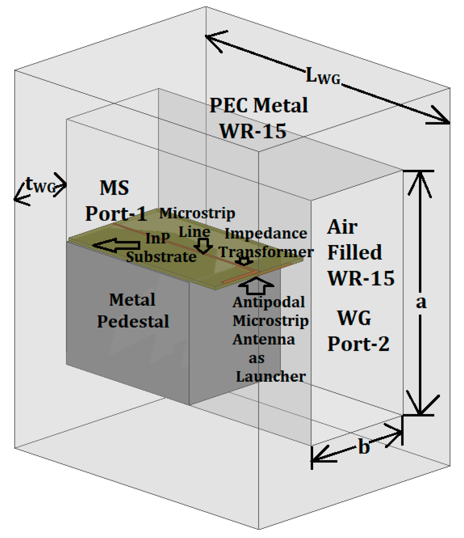
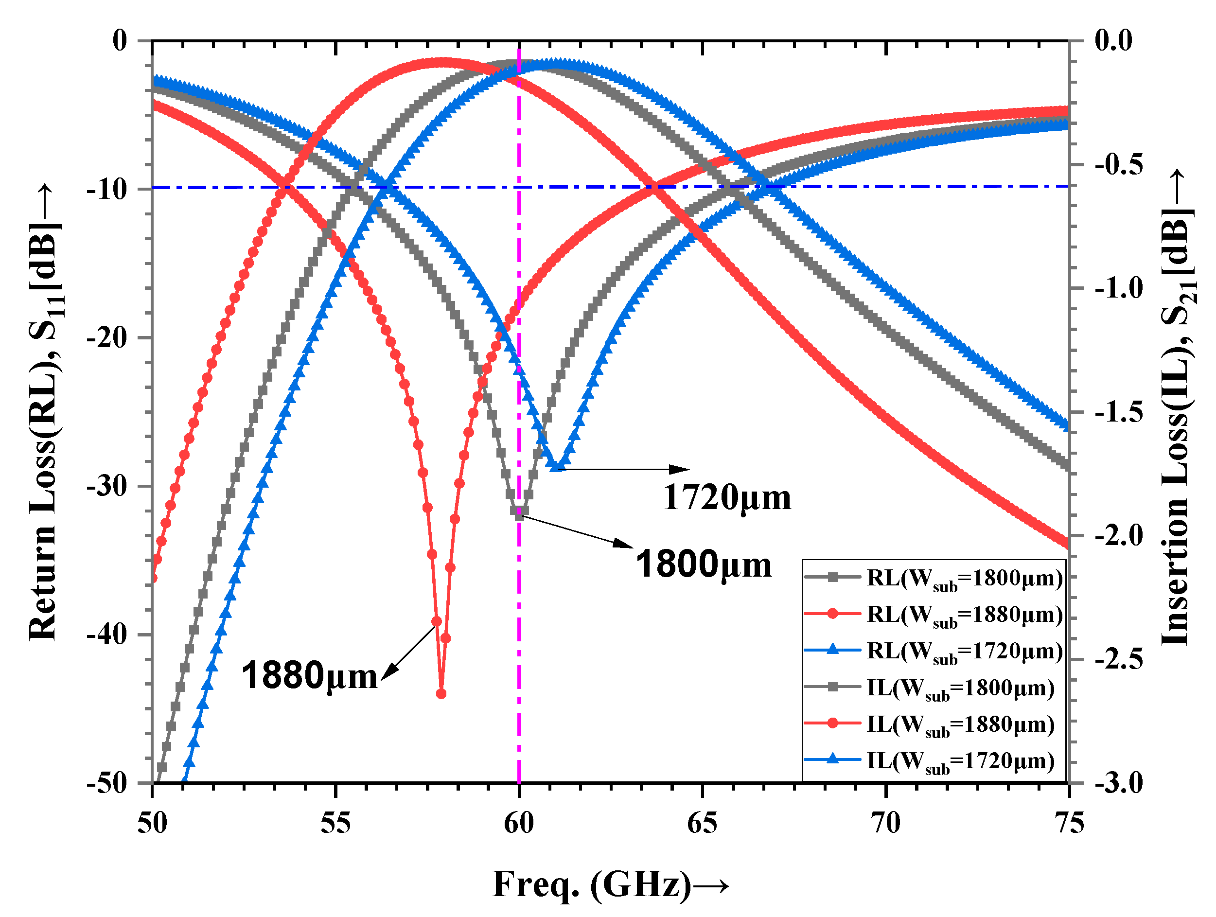
2.1. Substrate-Width Variations of V-Band Inline Transitions
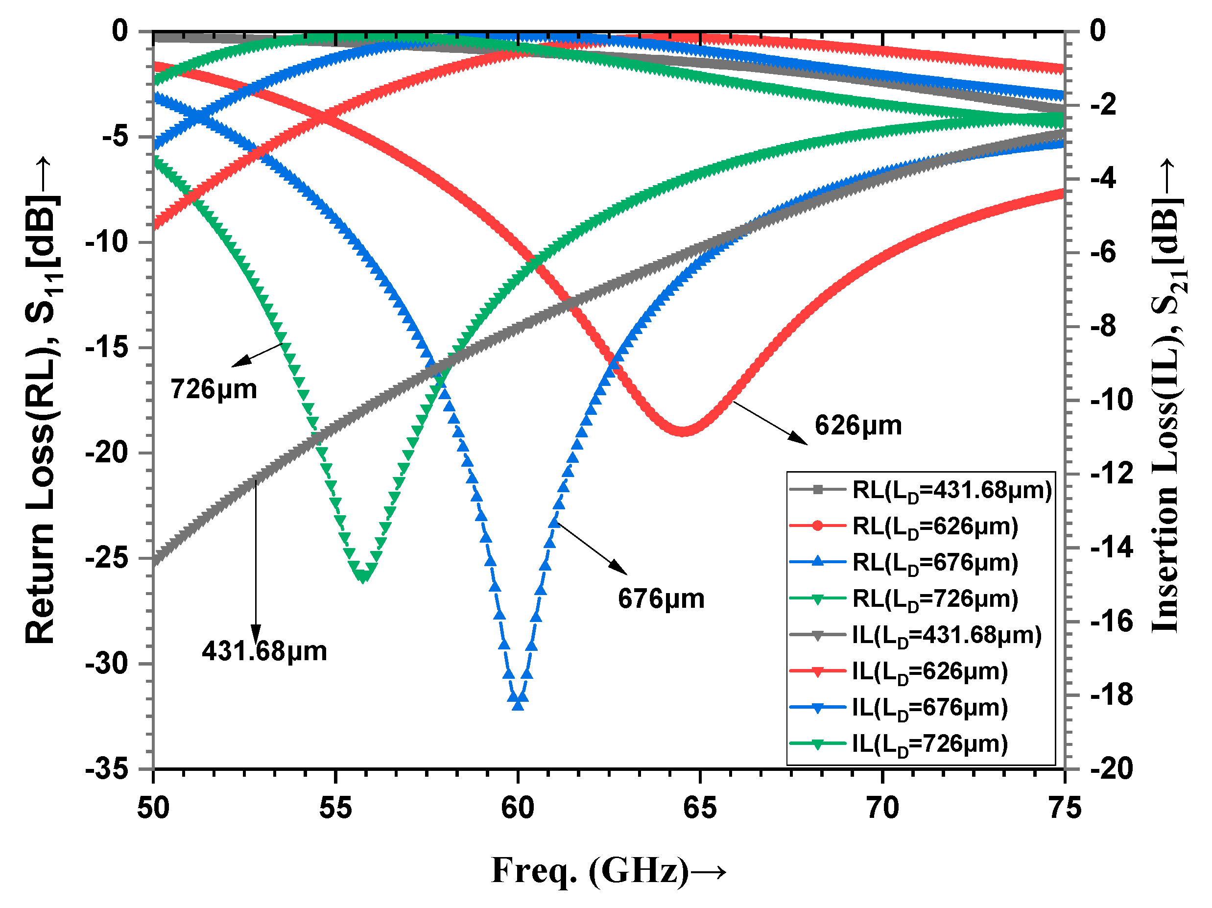
2.2. Length Variations of Dipole Antenna Arms
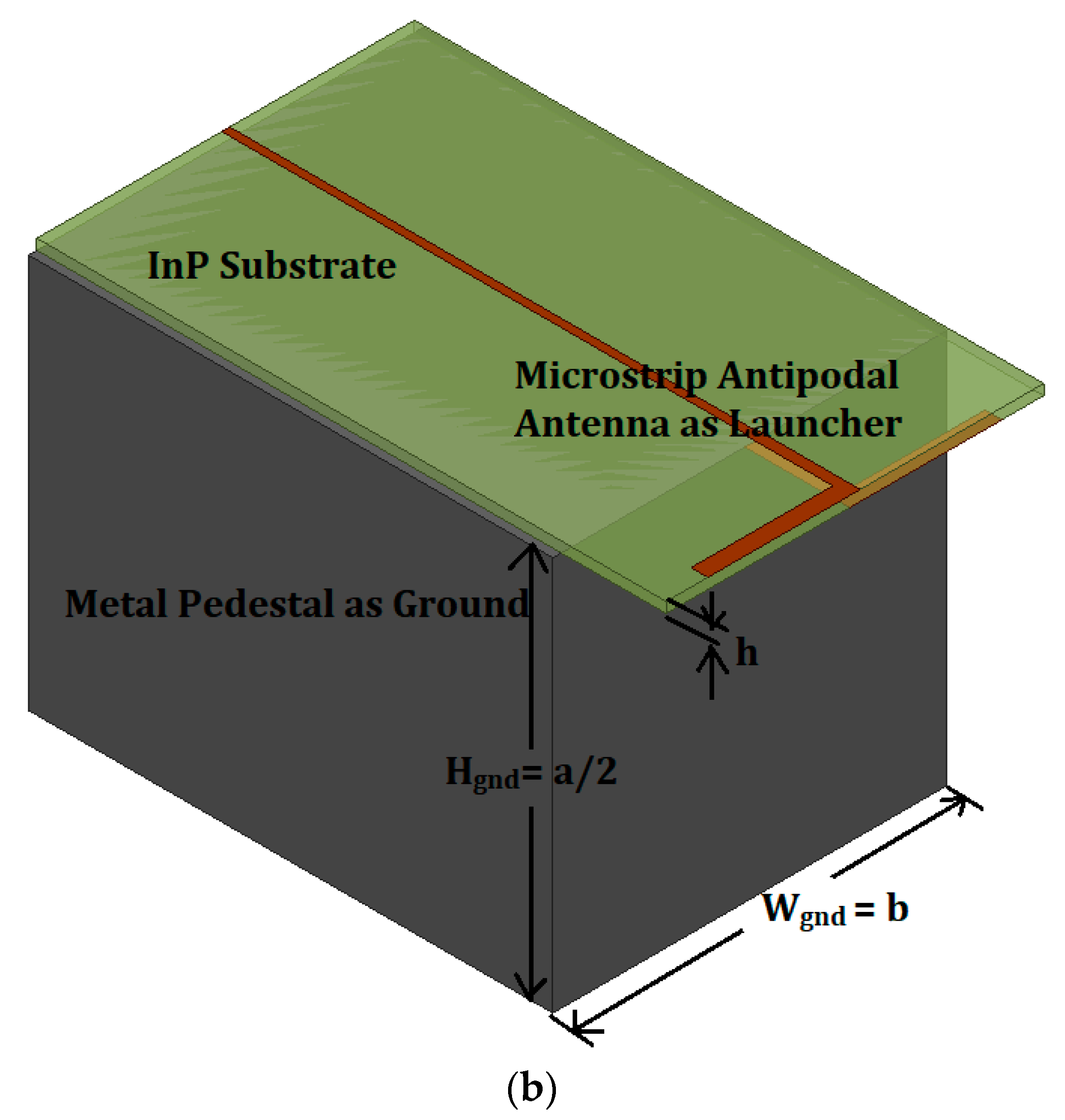
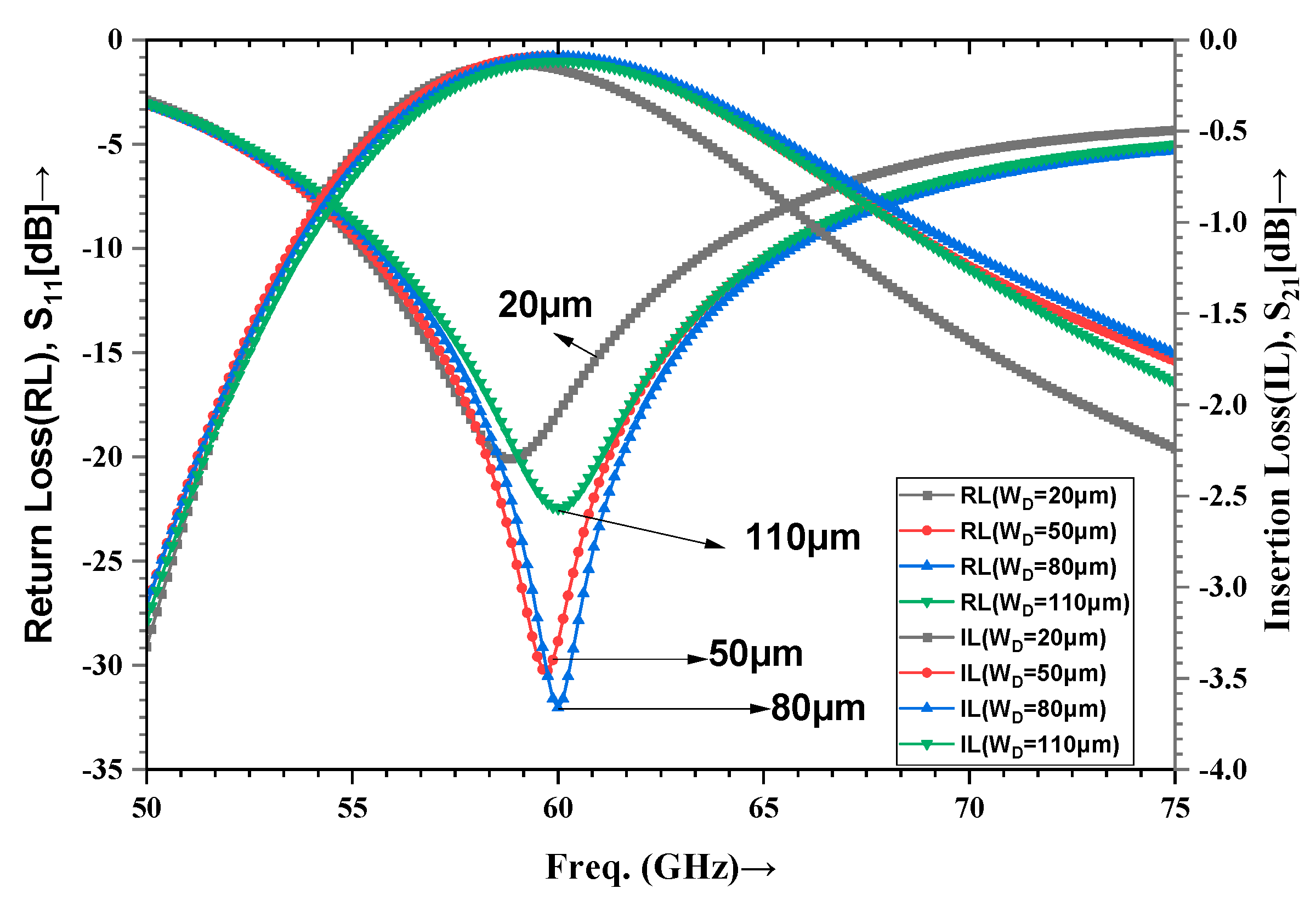
2.3. Width Variations of Dipole Antenna Arms
3. Results
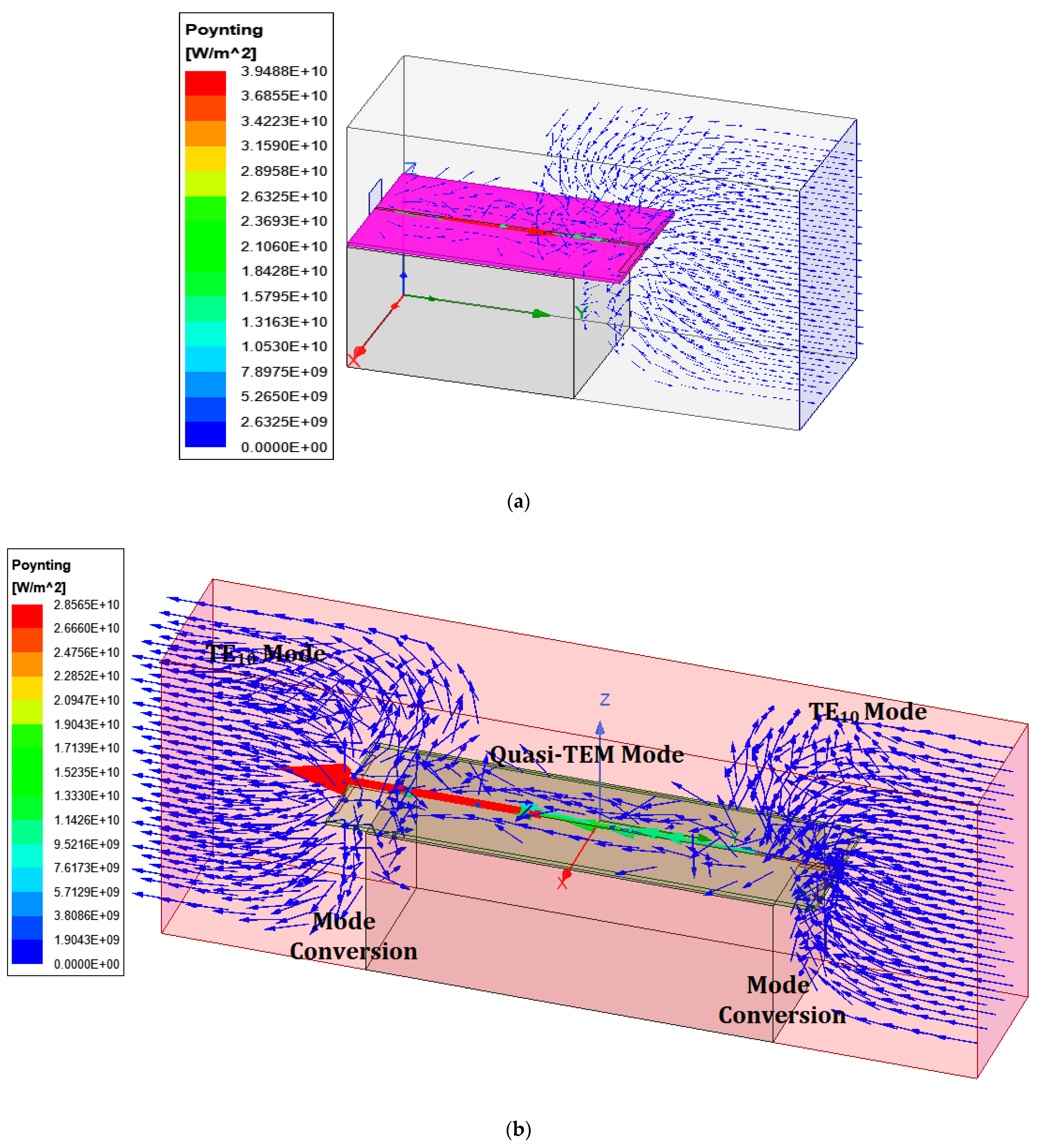
3.1. Power Flow in the Inline MS-to-WR-15 Transition
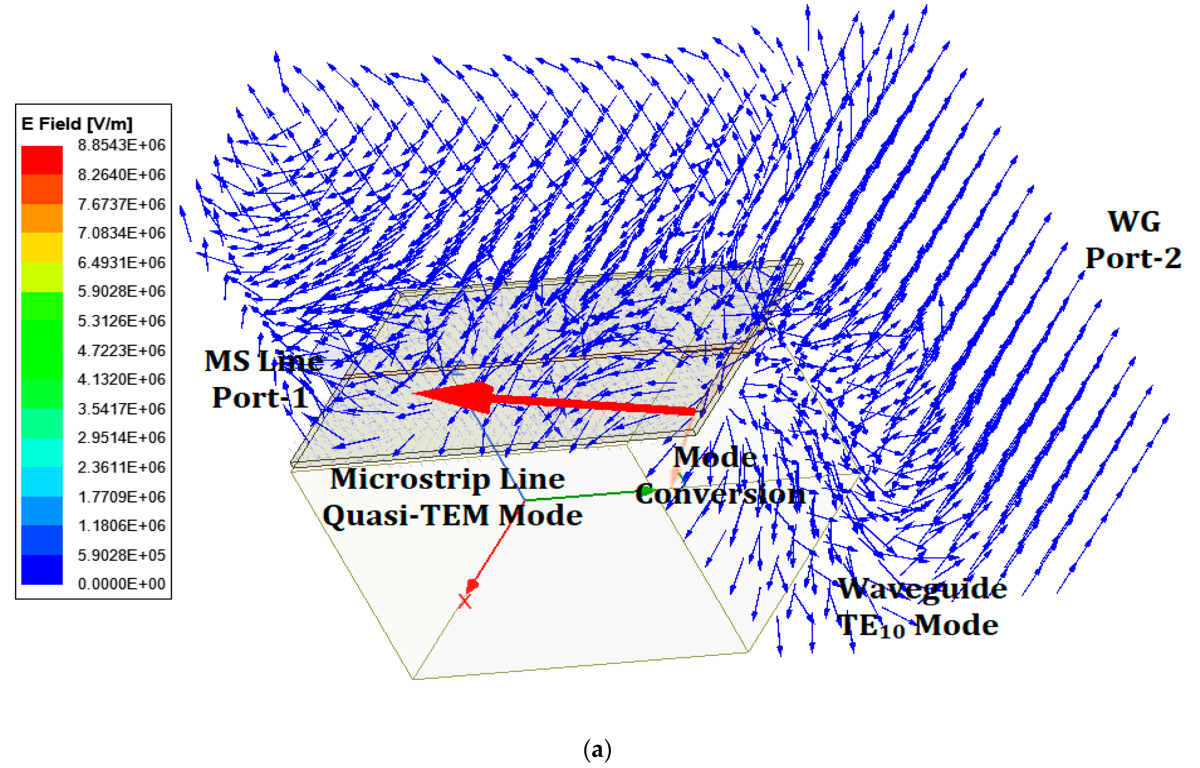
3.2. Electric Field Mode Conversion MS Line-to-RWG Inline V-Band Transition
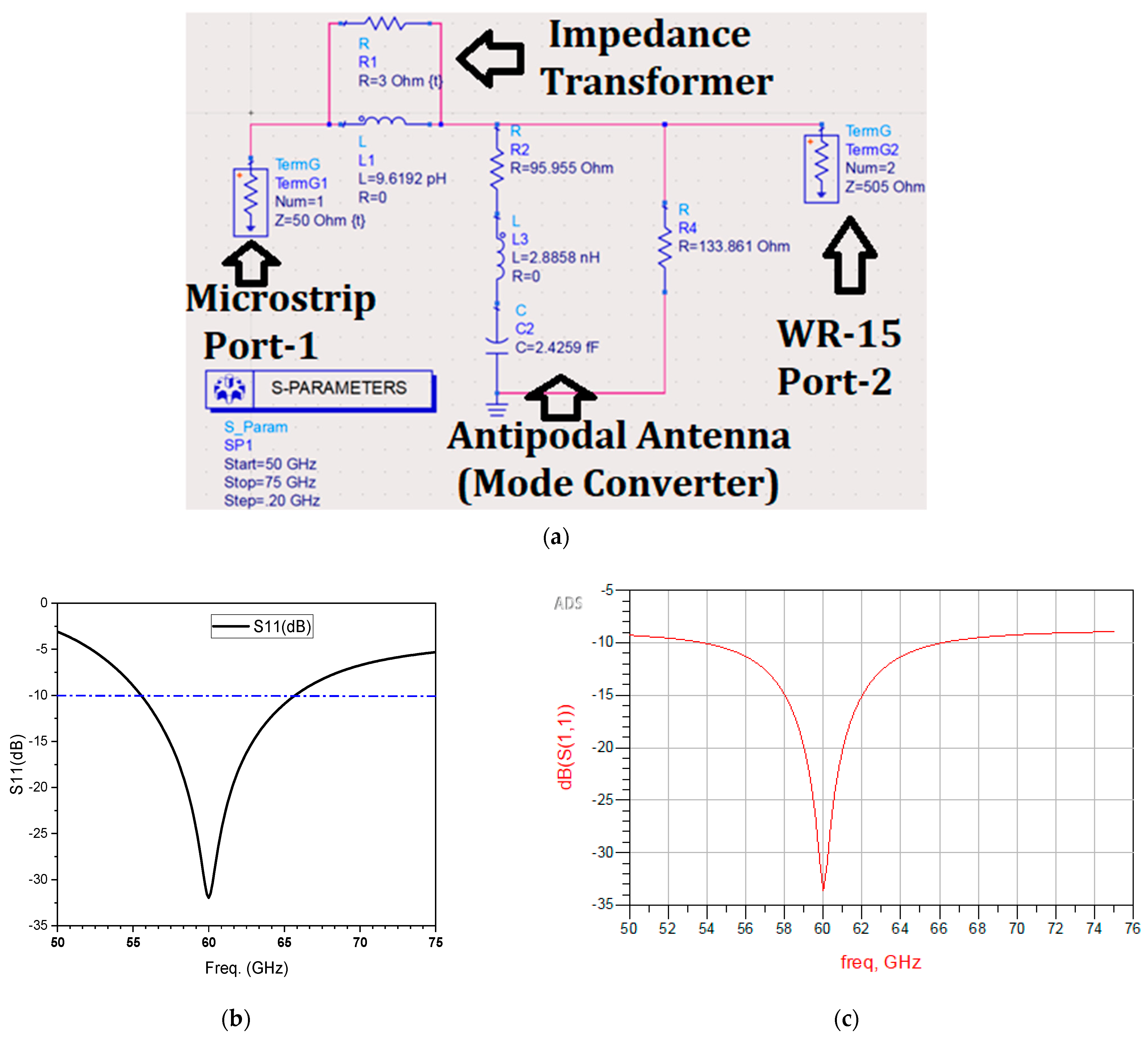
3.3. Equivalent Circuit of V-Band Transition Model
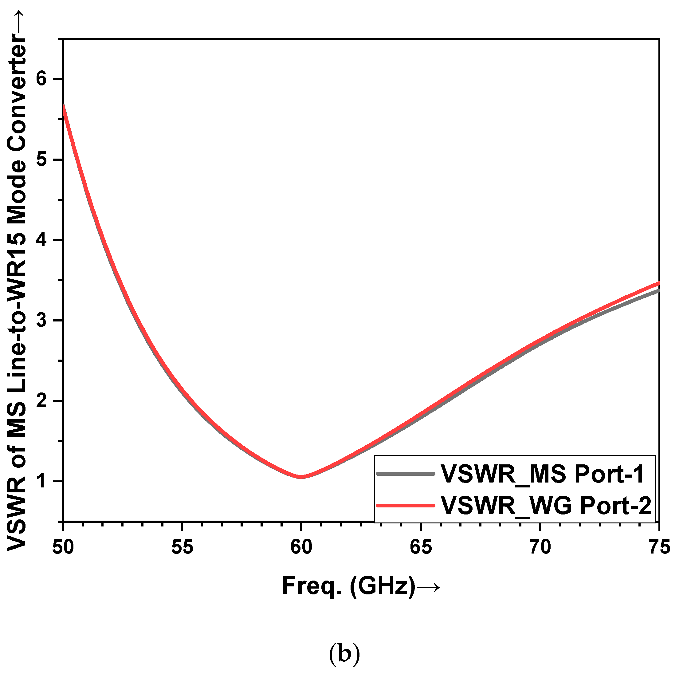
3.4. Performance Comparison of V-Band Transitions
4. Discussion
5. Conclusions
Author Contributions
Funding
Data Availability Statement
Acknowledgments
Conflicts of Interest
References
- Hassan, S.E.; Berggren, M.; Scheiner, B.; Michler, F.; Weigel, R.; Lurz, F. Design of planar microstrip-to-waveguide transitions using topology optimization. In Proceedings of the 2019 IEEE Radio and Wireless Symposium (RWS), Orlando, FL, USA, 20–23 January 2019; pp. 1–3. [Google Scholar]
- Ren, Y.; Li, K.; Wang, F.; Gao, B.; Wu, H. A broadband magnetic coupling microstrip to waveguide transition using complementary split ring resonators. IEEE Access 2019, 7, 17347–17353. [Google Scholar] [CrossRef]
- Huang, X.; Wu, K.-L. A broadband U-slot coupled microstrip-to-waveguide transition. IEEE Trans. Microw. Theory Technol. 2012, 60, 1210–1217. [Google Scholar] [CrossRef]
- Deslandes, D.; Wu, K. Integrated microstrip and rectangular waveguide in planar form. IEEE Microw. Wirel. Compon. Lett. 2001, 11, 68–70. [Google Scholar] [CrossRef]
- Pérez-Escudero, J.M.; Torres-García, A.E.; Gonzalo, R.; Ederra, I. A Gap Waveguide-based compact rectangular waveguide to a packaged microstrip inline transition. Appl. Sci. 2020, 10, 4979. [Google Scholar] [CrossRef]
- Pérez, J.M.; Rebollo, A.; Gonzalo, R.; Ederra, I. An inline microstrip-to-waveguide transition operating in the full W-Band based on a Chebyshev multisection transformer. In Proceedings of the European Conference on Antennas and Propagation (EuCAP), Davos, Switzerland, 10–15 April 2016; Volume 10, pp. 1–4. [Google Scholar]
- Pérez-Escudero, J.M.; Torres-García, A.E.; Gonzalo, R.; Ederra, I. A simplified design inline microstrip-to-waveguide transition. Electronics 2018, 7, 215. [Google Scholar] [CrossRef]
- Simone, M.; Fanti, A.; Valente, G.; Montisci, G.; Ghiani, R.; Mazzarella, G. A compact in-line waveguide-to-microstrip transition in the Q-Band for radio astronomy applications. Electronics 2018, 7, 24. [Google Scholar] [CrossRef]
- Li, C.L.; Jin, C.; Ma, H.Q.; Shi, X.W. An inline waveguide-to-microstrip transition for wideband millimeter-wave applications. Microw Opt. Tech Lett. 2015, 62, 1516–1520. [Google Scholar] [CrossRef]
- Hügler, P.; Chaloun, T.; Waldschmidt, C. A wideband differential Microstrip-to-Waveguide Transition for multilayer PCBs at 120 GHz. IEEE Microw Wirel. Compts Lett. 2020, 30, 170–172. [Google Scholar] [CrossRef]
- Kaneda, N.; Qian, Y.; Itoh, T. A broad-band Microstrip-to-Waveguide Transition using quasi-Yagi Antenna. IEEE Trans. Microw. Theory Techn. 1999, 47, 2562–2567. [Google Scholar] [CrossRef]
- Van Heuven, J.H.C. A new integrated Waveguide-Microstrip Transition. IEEE Trans Microw Th. Tech. 1976, 24, 144–147. [Google Scholar] [CrossRef]
- Lou, Y.; Chan, C.H.; Xue, Q. An in-line Waveguide-to-Microstrip Transition using radial-shaped probe. IEEE Microw Wirel. Compts Lett. 2008, 18, 311–313. [Google Scholar] [CrossRef]
- Tang, C.; Pan, X.; Cheng, F.; Lin, X. A broadband Microstrip-to-Waveguide end-wall probe transition and its application in waveguide termination. Progr. Electromagnet Res. Lett. 2020, 89, 99–104. [Google Scholar] [CrossRef]
- Varshney, A.K. A microwave rectangular waveguide-to-microstrip line transitions @30 GHz. Inter. J. Emerg. Tech. Ad. Eng. 2013, 3, 1–6. [Google Scholar]
- Gupta, R.; Kumar, P.P. Improved design of Ka-band waveguide to coaxial right angle microwave transition. In Proceedings of the 2020 URSI Regional Conference on Radio Science (URSI-RCRS), Varanasi, India, 12–14 February 2020. [Google Scholar]
- Ariffin, A.; Isa, D. Bandwidth enhancement of microstrip line-to-waveguide transitions for broadband E-band module applications. Microw. Opt. Tech. Lett. 2016, 58, 1398–1401. [Google Scholar] [CrossRef]
- Shih, Y.C.; Ton, T.N.; Bui, L.Q. Waveguide-to-Microstrip Transitions for mm-wave applications. In Proceedings of the IEEE MTT-S International Microwave Symposium Digest, New York, NY, USA, 25–27 May 1988; pp. 473–475. [Google Scholar]
- Murphy, E.R. Microstrip to Waveguide Transition. U.S. Patent 4453142, 5 June 1984. [Google Scholar]
- Lin, T.-H.; Wu, R.-B. A Broadband Microstrip-to-Waveguide transition with tapered CPS probe. In Proceedings of the 32nd European Microwave Conference, Milan, Italy, 23–26 September 2002; pp. 1–4. [Google Scholar]
- Varshney, A.; Sharma, V. A comparative study of microwave rectangular waveguide-to-microstrip line transition for millimeter wave, wireless communications and radar applications. Microw. Rev. 2020, 2, 26–37. [Google Scholar]
- Sakakibara, K.; Hirono, M.; Kikuma, N.; Hirayama, H. Broadband and planar microstrip-to-waveguide transitions in mm-wave band. In Proceedings of the 2008 International Conference on Microwave and Millimeter Wave Technology, Nanjing, China, 21–24 April 2008; pp. 1278–1281. [Google Scholar]
- Aliakbarian, H.; Enayati, A.; Vandenbosch, G.A.E.; De Raedt, W. Novel Low-Cost End-Wall Microstrip-To-Waveguide Splitter Transition. Prog. Electromagn. Res. 2010, 101, 75–96. [Google Scholar] [CrossRef][Green Version]
- Kumari, S.; Mondal, P. Full U-Band Rectangular Waveguide-to-Microstrip Transition Using E-Plane Probe. In Proceedings of the 11th International Radar Symposium India—2017, Bangalore, India, 12–16 December 2017; pp. 1–4. [Google Scholar]
- Balani, C.A. Antenna Theory, 4th ed.; Wiley: New York, NY, USA, 2016. [Google Scholar]
- Pozar, D.M. Microwave Engineering, 4th ed.; Wiley: New York, NY, USA, 2016; pp. 148–149. [Google Scholar]
- Varshney, A.; Cholake, N.; Sharma, V. Low-cost ELC-UWB fan-shaped antenna using parasitic SRR triplet for ISM band and PCS applications. Int. J. Electron. Lett. 2021, 10, 391–402. [Google Scholar] [CrossRef]
- Liao, S.Y. Microwave Devices and Circuits, 3rd ed.; Pearson Prentice Hall: Hoboken, NJ, USA, 2007. [Google Scholar]
- Theraja, B.L. A Textbook of Electrical Technology (Basic Electrical Engineering); S. Chand Publishing: New Delhi, India, 2005; Volume 1. [Google Scholar]
- Zhou, I.; Robert, J.R. Ultra-Wideband Narrow Wall Waveguide-to-Microstrip Transition Using Overlapped Patches. Sensors 2022, 22, 2964. [Google Scholar] [CrossRef] [PubMed]
- Han, K.Y.; Pao, C. A V-band waveguide to microstrip inline transition. In Proceedings of the IEEE/MTT-S International Microwave Symposium Digest, Montreal, QC, Canada, 17–22 June 2012; pp. 1–3. [Google Scholar]
- Mozharovskiy, A.V.; Soykin, O.V.; Artemenko, A.A.; Maslennikov, R.O.; Vendik, I.B. Wideband Wave-guide-to-Microstrip Transition for mm-Wave Applications. J. Russ. Universities. Radioelectron. 2019, 22, 17–32. [Google Scholar] [CrossRef]
- Xu, Z.; Xu, J.; Qian, C. Novel In-Line Microstrip-to-Waveguide Transition Based on E-Plane Probe T-Junction Structure. IEEE Microw. Wirel. Compon. Lett. 2021, 31, 1051–1054. [Google Scholar] [CrossRef]
- Henderson, J.R.; Walden, M.C. Microstrip-to-Waveguide Transition for 3D-Printed mm-Wave Sectoral Horn Array. In Proceedings of the 16th European Conference on Antennas and Propagation (EuCAP), Madrid, Spain, 27 March–1 April 2022; pp. 1–3. [Google Scholar]


| Parameter Name | Parameter Designation | Dimensions Values (μm) |
|---|---|---|
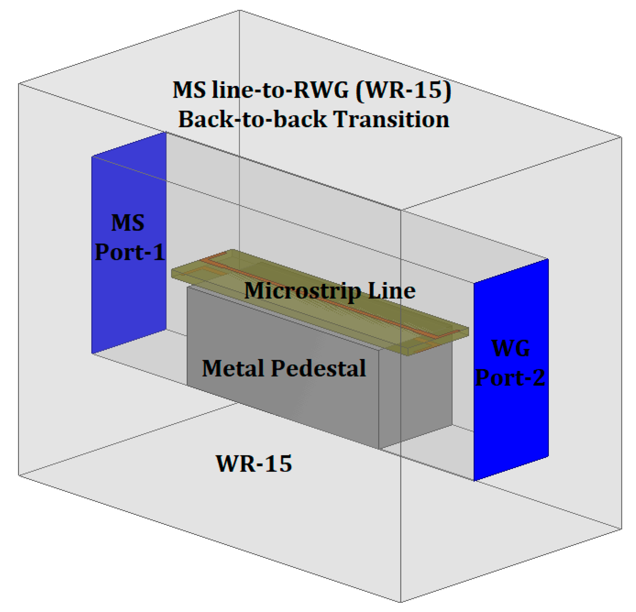
| RWG | WR-15 inner dimensions: Breadth: a Width: b Length: LWG Thickness: tWG | WR-15 inner dimensions: a: 3760 b: 1880 LWG: 5000 tWG: 1015 |
| PEC Metal Pedestal (Ground) | Width: Wgnd Height: Hgnd Length: Lgnd | 1880 1880 |
| Substrate | Width: Wsub Length: Lsub Height: Hsub | Wsub: b-80 = 1800 Hsub: 50 |
| 50Ω MSL | Feed width: Wf Feed length: Lf Thickness: t | Wf: 37.79 Lf: 2500 t: 400nm (gold) |
| Impedance Transformer | TF width: Wt TF length: Lt Thickness: t | Wt: 50 Lt: 500 t: 400 nm (gold) |
| Microstrip Dipole Antipodal Antenna | Dipole arms: Width: WD Length: LD Thickness: t | Probe/dipole: WD: 80 LD: 676 t: 400 nm (gold) |
| Substrate Width, Wsub (μm) | Tuning Frequency (GHz) | RL (dB) | IL (dB) | −10dB Bandwidth (GHz) |
|---|---|---|---|---|
| 1720 | 61.07 | −28.75 | −0.10 | 56.48–66.79 |
| 1800 | 60 | −32.05 | −0.09 | 55.54–65.72 |
| 1880 | 57.90 | −44.19 | −0.09 | 53.73–63.64 |
| Dipole Antenna Arms’ Length, LD (μm) | Tuning Frequency (GHz) | RL (dB) | IL (dB) | −10 dB Bandwidth (GHz) |
|---|---|---|---|---|
| 431.68 | ---------- | ---------- | ---------- | ---------- |
| 626 | 64.57 | −19.06 | −0.15 | 59.90–70.79 |
| 676 | 60 | −32.05 | −0.09 | 55.54–65.72 |
| 726 | 55.75 | −25.88 | −0.10 | 52.06–61.22 |
| Dipole Antenna Arms Width, WD (μm) | Tuning Frequency (GHz) | RL (dB) | IL (dB) | −10 dB Bandwidth (GHz) |
|---|---|---|---|---|
| 20 | 58.82 | −20.08 | −0.13 | 55.19–63.73 |
| 50 | 64.57 | −30.41 | −0.09 | 55.33–65.40 |
| 80 | 60 | −32.05 | −0.09 | 55.54–65.72 |
| 110 | 60 | −22.47 | −0.12 | 55.74–65.35 |
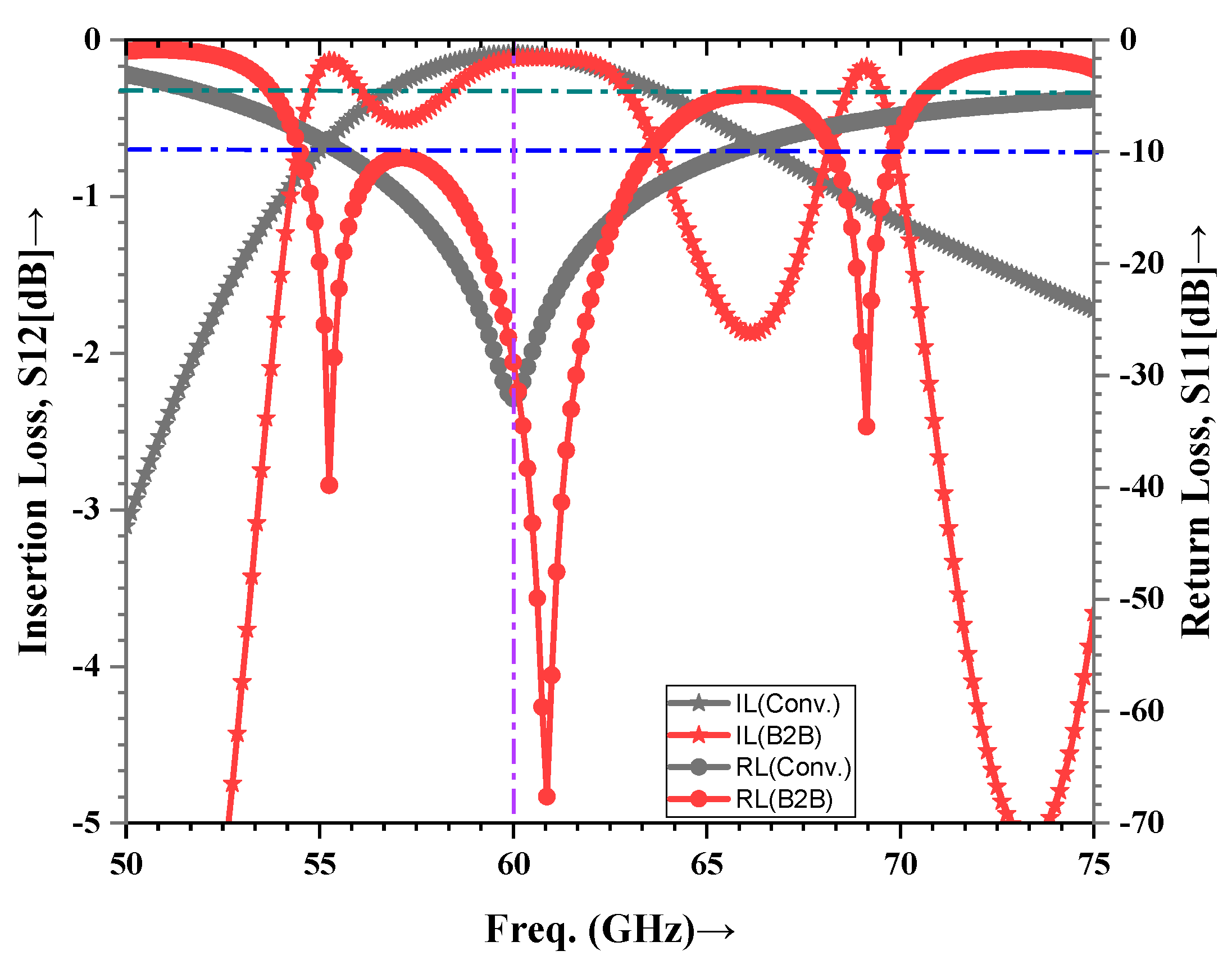
| MS-to-RWG Transition | Res. Freq. f0 (GHz) | IL (dB) | RL (dB) | FBW (%) |
|---|---|---|---|---|
| Conventional | 60 | −0.09 | −32.05 (Port-1) −31.45 (Port-2) | 17 (Port-1) (55.57–65.76 GHz) 10.6 (Port-2) (55.67–65.49 GHz) |
| Back-to-Back | 55.25 60.87 69.13 | −0.13 −0.12 −0.18 | −39.77 −67.35 −35.36 | (54.49–63.53 GHz) and (68.25–69.83 GHz) |
| Ref. | Substrate Used for MSL | RWG Type (‘a’ mm × ‘b’ mm) and WallThickness (t mm) | RL < (dB) | IL > (dB) | FBW (%) | Coupling Method and Features |
|---|---|---|---|---|---|---|
| [18] Shih, Y. C. et al. 1988 | RT-Duriod 5880 h = 0.127 mm tanδ ≈ 0.0009 at 10 GHz | WR-12 (3.10 × 1.55) t = 1.015 | −12 | −1.0 | 40 (relative BW) | .Transverse (90°) .Microstip probe as launcher .Aperture cut |
| [23] Aliakbarian et al. 2010 | Rogers RT/Duroid 5880 h = 0.254 mm tanδ = 0.0009 10 GHz | WR-15 (3.76 × 1.88) t = 1.015 | −17 | −4.0 | 37.7 | .End-wall .Consists of an end-wall .A double-sided etched substrate .Slot coupling |
| [25] Zhou, I., and Robert, J. R. 2022 | RO4003 h = 0.81 mm | WR-34 (4.5 × 8.8) t = 2.0 | −17, −30 | −0.67, −0.85 | 21.2, 23 | .Inline .LMDS, Ka-band operation for 5G applications |
| [26] Kyu, Y.H. and Pao, C. 2012 | Quartz h = 0.127 mm | WR-15 (3.76 × 1.88) t = 1.015 | −37 | −0.7 (B2B) −0.35 (conv.) | 35.2 | .Inline (E-plane) .Five-step ridge waveguide .Probe fed .Broad band |
| [27] Mozharovskiy A. V., 2019 | RO4350B H = 0.101 mm at 60 GHz RT/Duroid 5880 H = 0.127 mm at 60 GHz | WR-15 (3.76 × 1.88) t = 1.015 | −10 −10 | −1.1 −0.4 | 11.2 20 | .Transverse B2B .Low loss .Wideband .Uses 25 via |
| [28] Xu, Z. et al. 2021 | Quartz h = 0.127mm | WR-10 (2.54 × 1.27) t = 1.015 | −18 | −0.35 to −0.5 | 31.89 | .W-band inline B2B E-plane probe T-junction structure .mm-wave applications |
| [29] Henderson, J. R. and Walden, M. C. 2022 | RT/Duroid 5880 h = 0.127mm | WR-15 (3.76 × 1.88) t = 1.015 | −10 | −1.0 | 21.87 | .Inline .PCB transition .Highly integrated with mm-wave beam-forming devices .3D-printed mm-wave sectoral horn array |
| This work | InP h = 50 μm at 60GHz | WR-15 (3.76 × 1.88) t = 1.015 | −30 | −0.09 | 40.76 (relative BW) | .Inline (0°) .Dipole antipodal antenna as launcher .Double-sided etched InP substrate |
Publisher’s Note: MDPI stays neutral with regard to jurisdictional claims in published maps and institutional affiliations. |
© 2022 by the authors. Licensee MDPI, Basel, Switzerland. This article is an open access article distributed under the terms and conditions of the Creative Commons Attribution (CC BY) license (https://creativecommons.org/licenses/by/4.0/).
Share and Cite
Varshney, A.; Sharma, V.; Elfergani, I.; Zebiri, C.; Vujicic, Z.; Rodriguez, J. An Inline V-Band WR-15 Transition Using Antipodal Dipole Antenna as RF Energy Launcher @ 60 GHz for Satellite Applications. Electronics 2022, 11, 3860. https://doi.org/10.3390/electronics11233860
Varshney A, Sharma V, Elfergani I, Zebiri C, Vujicic Z, Rodriguez J. An Inline V-Band WR-15 Transition Using Antipodal Dipole Antenna as RF Energy Launcher @ 60 GHz for Satellite Applications. Electronics. 2022; 11(23):3860. https://doi.org/10.3390/electronics11233860
Chicago/Turabian StyleVarshney, Atul, Vipul Sharma, Issa Elfergani, Chemseddine Zebiri, Zoran Vujicic, and Jonathan Rodriguez. 2022. "An Inline V-Band WR-15 Transition Using Antipodal Dipole Antenna as RF Energy Launcher @ 60 GHz for Satellite Applications" Electronics 11, no. 23: 3860. https://doi.org/10.3390/electronics11233860
APA StyleVarshney, A., Sharma, V., Elfergani, I., Zebiri, C., Vujicic, Z., & Rodriguez, J. (2022). An Inline V-Band WR-15 Transition Using Antipodal Dipole Antenna as RF Energy Launcher @ 60 GHz for Satellite Applications. Electronics, 11(23), 3860. https://doi.org/10.3390/electronics11233860