1. Introduction
With the advent of super-junction technology, the trade-off characteristic between breakdown voltage (BV) and specific on-resistance (R
on) in silicon-based power devices has dramatically improved [
1,
2]. Therefore, power-device manufacturing for higher voltages and currents can be realized. As one of the beneficiaries, vertical double-diffused MOSFETs (VDMOSFETs) have been extremely successful in the high-voltage power-conversion market due to the improvement of the theoretical limit of silicon (R
on·A∝BV
2.5) [
3,
4]. At present, Super-Junction VDMOSFET (SJ-VDMOSFET) has become a sole dominant flagship technology in the field of high-power switching and inverter systems where its blocking voltage is required in the range of 600–900 V [
3]. Nevertheless, the switching performance of SJ-VDMOSFETs is significantly limited under high-frequency operation due to the long minority-carrier lifetime of silicon chips. Consequently, in order to realize the improvement of the comprehensive performance of SJ-VDMOSFETs, the minority-carrier lifetime of the devices must be reduced properly by utilizing some lifetime control techniques. The underlying mechanism of these techniques to reduce minority carrier lifetime is the introduction of recombination centers in silicon devices.
Currently, the lifetime control techniques are mostly divided into two categories: (I) introducing heavy metal impurities in the chip-manufacturing process, such as gold [
5], palladium [
6], platinum [
7], and so on; (II) high-energy (MeV) radiation, such as electron irradiation [
8,
9] and Co
60 gamma irradiation [
10]. For the first technique, owing to the inferior controllability of the diffusion process for heavy metal impurity and nonuniform distribution of diffusing impurity, the power devices possess the disadvantages of high leakage current and the poor blocking characteristics of high temperature. Therefore, this technique is not recommended for practical manufacturing processes. On the contrary, the second technique can accurately modulate the minority-carrier lifetime of the power devices by controlling the implantation dose; thus, the comprehensive performance of the power devices can be optimized. Furthermore, this technique greatly simplifies the manufacturing processes and design complexity of the power devices because it is used after device fabrication. Accordingly, high-energy radiation is widely used in the manufacture of power-switching devices, especially electron irradiation. Nevertheless, electron irradiation results in the buildup of oxide-trapped charge and the generation of interface traps [
11,
12], which severely influence the stability of electrical characteristics and reliability of MOS devices [
13]. In particular, the negative shift of threshold voltage (V
th) after the electron irradiation is the most serious problem for the commercial MOS devices because the operation mode of devices may be changed from enhancement mode to depletion mode, thus leading to a possible failure of power system. In order to explore the basic mechanism of degradation of the V
th, an enormous number of studies have been conducted and abundant achievements have been reported [
14,
15,
16,
17,
18,
19,
20,
21]. However, the basic mechanism of radiation-induced degradation of the V
th in the SJ-VDMOSFET devices is still lacking. Meanwhile, previous studies mainly focus on an experimental level of influence mechanism and the relationship between the radiation dose and the V
th, but a deep-level theoretical research on the atomic scale has not been taken into account. Consequently, the degradation mechanism of the V
th caused by the electron irradiation and the recovery of the irradiated super-junction devices are worth investigating to meet the scientific research and commercial applications.
In this article, a study for the irradiation-induced degradation on the transfer characteristics (ID–VG) of SJ-VDMOSFETs is conducted, focusing on the recovery of the irradiated devices and the degradation mechanism in the atomic scale. It is found that the Vth of SJ-VDMOSFETs after electron irradiation can be recovered by applying a high gate-bias voltage at a suitable amount of time. The recovery level significantly increases with the decrease in the applied gate voltage and the multiplication of stress time. Moreover, a high temperature of 175 °C does not play a facilitating role in the recovery process. According to the density of states of the Si/SiO2 interface, we find that new electronic states will be generated in the conduction bands and valence bands due to the fracture of the Si-H/-OH bonds induced by high-energy electrons. Their distribution is related to the passivation of the Si/SiO2 interface. In addition, the quantitative relationship between the interface charge density (Qss) and threshold variation (∆Vth) is also taken into account. The result clearly shows that the response of the threshold variation to the increasing multiples of interface charge density is a linear behavior.
2. Experimental and Computational Methods
The silicon-based Super-Junction VDMOSFET (
N-channel) devices investigated in this article are fabricated by the same manufacturing process. The schematic diagram of two half-cells of SJ-VDMOSFET is shown in
Figure 1. In detail, the chip size of the device is 0.049 cm
2. The thickness of the gate oxide layer of the device is 80 nm. In addition, the V
th of the pristine SJ-VDMOSFET is 3.5 V and 2.1 V at 25 °C and 175 °C, respectively (Test condition: V
DS = V
GS, I
DS = 250 uA). For the irradiation experiment, the SJ-VDMOSFET chips were irradiated by using a high-energy electron source to a total dose of 50 kGy. Among them, we applied the irradiation experiment to 100 SJ-VDMOSFETs in the form of TO-220F outline package. Subsequently, we selected postirradiation SJ-VDMOSFETs with similar V
th (with an error of no more than 0.05 V) for recovery experiments and selected 10 SJ-VDMOSFETs with typical rules for discussion and analysis. For the recovery experiment, a high gate voltage was applied to the postirradiation SJ-VDMOSFETs, whereas source and drain were grounded at room temperature. In order to determine a critical voltage applied on gate, the voltage was gradually increased by an interval of 1 V. Simultaneously, since the reliability of the gate oxide may degrade under high electric-field stress, the time of electric-field stress applied on the gate should be considered. Additionally, the postirradiation SJ-VDMOSFETs were analyzed at room temperature of 25 °C and high temperature of 175 °C, respectively, to demonstrate the effect of temperature on the recovery of the irradiated devices. The theoretical models used for device performance calibration before and after ion irradiation included mobility models (Doping Dependence and High Field Saturation), recombination models (Shockley Read Hall and Auger), and effective intrinsic density model (OldSlotboom). In addition, the most important HeavyIon model was considered. The static characteristics of the irradiated devices were measured by ADVANTEST V93000 SOC.
In order to obtain an insight into the degradation mechanism of the I
D-V
G in the atomic scale, the quantum mechanical calculations within the framework of density functional theory (DFT) were performed by using DMol
3 package, as implemented in Materials Studio [
21,
22]. The exchange–correlation density functional is described by employing the generalized gradient approximation (GGA) in the form of Perdew–Burke–Emzerhof (PBE) parameterization [
23,
24]. The full relaxation of atomic positions and lattice constants of Si/SiO
2 interface were conducted by adopting the double numerical plus polarization (DNP) basis set with the global cutoff of 5.0 Å. The convergence tolerance of energy and force on each atom were set to be 10
−5 eV and 0.002 eV/Å, respectively. For the long-range van der Waals interactions in the Si/SiO
2 interface, the dispersion-corrected density functional theory (DFT-D) approach proposed by Grimme was adopted to effectively remedy the deficiency of the standard PBE functional [
25,
26]. A vacuum space of 15 Å was placed on the top and bottom of Si/SiO
2 interface to ensure no spurious interaction between the periodic interfaces in the direction perpendicular to the SiO
2 (0 1 0) plane. The Monkhorst–Pack k-point sampling in the Brillouin zone was set to be 9 × 9 × 4 for structural optimization and 13 × 13 × 4 for electronic structure calculations. Moreover, a technology computer-aided designed (TCAD) simulation was performed to confirm the relationship between the increasing multiples of interface charge density (∇Q
ss) and ∆V
th.
3. Results and Discussion
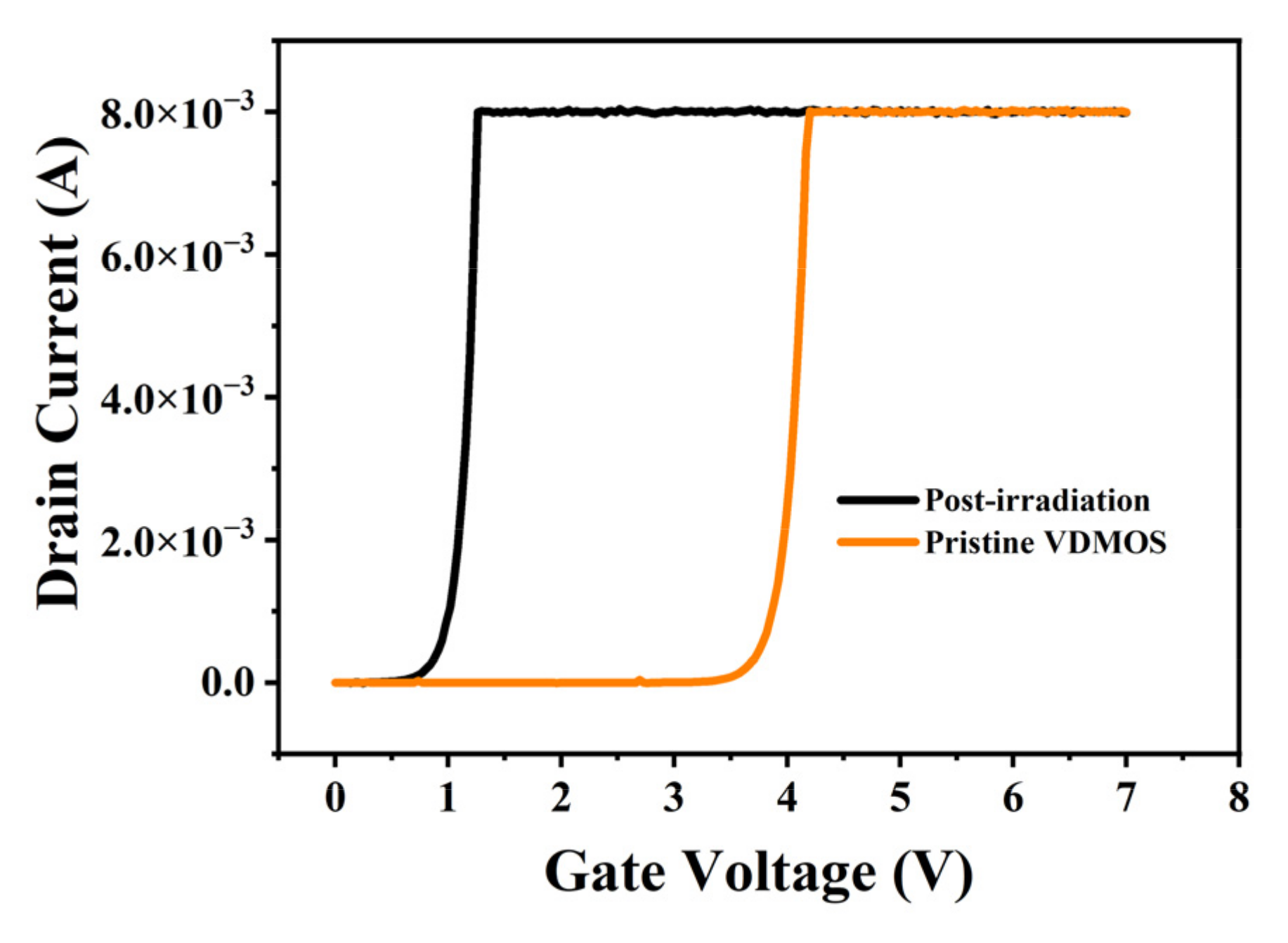
In
Figure 2, as observed in the irradiation experiment, it can be seen that the I
D-V
G curves shift toward the direction of the gate voltage, decreasing after the electron irradiation (a total dose of 50 kGy), which indicates that the operational reliability of SJ-VDMOSFETs will deteriorate due to the decrease in the V
th. Moreover, the V
th of the irradiated devices is less than 0.9 V, which is 2.7 V smaller than that of the pristine devices. In the case of large-dose irradiation, the interface traps and oxide traps increase, and the threshold voltage of the device shifts due to their combined effect. Following the introduction of a high electric-field stress at the gate, the purpose of our experiment is to fill the interface traps and oxide traps induced by irradiation with electrons to recover the V
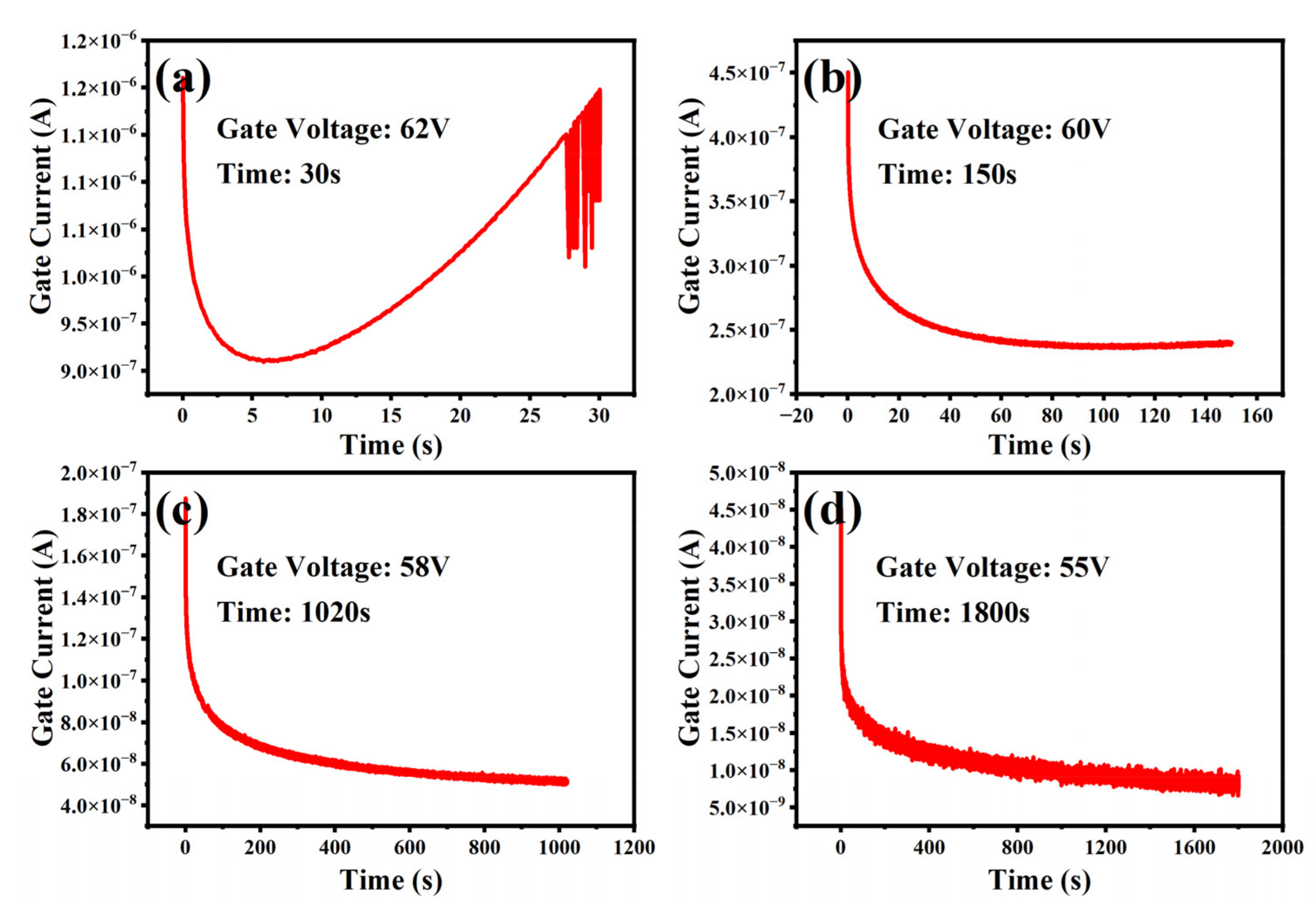
th of the irradiated device to the initial level. In order to explore the relationship between the electric-field stress and stress time, a tremendous amount of testing was performed. Interestingly, for the case of gate voltage of 62 V, the leakage current of the gate dramatically decreases within the range of 0 s to 6 s, whereas it exhibits a nonlinear increasing trend when the stress time continues to increase from 6 s to 30 s, as depicted in
Figure 3a. Considering the fluctuation of the gate oxide-layer thickness in the gate oxide-layer growth process, when the gate voltage is applied to 62 V, the charging process of the gate capacitor is completed within 0 s to 6 s. Subsequently, part of the gate oxide layer reaches its limit electric-field strength (10 MV/cm) and is broken down. This is also the main reason why the leakage current of the device exhibits a nonlinear increasing trend. On the contrary, when the applied gate bias is 60 V, the leakage current rapidly decreases in the range of 0 s to 20 s and then gradually stabilizes with the increase in stress time, as illustrated in
Figure 3b. The stress time of applying bias voltage at the gate is five times longer than that in the case of 62 V. Simultaneously, a similar variation tendency for the leakage current of gate is also observed in two cases where the applied gate biases are 58 V [
Figure 3c] and 55 V [
Figure 3d], respectively. However, it should be noted that the leakage current still presents a downward trend after the bias voltage (58 V or 55 V) is applied at the gate for a long stress time. In a word, the time duration of the electric-field stress applied at the gate has a relationship of negative correlation with the magnitude of gate voltage. In addition, owing to a decrease of 2 V or 3 V in the applied gate bias, the stress time needs to be increased by at least twice. Therefore, it is extremely important to determine an appropriate gate voltage and the corresponding stress time for the recovery of irradiated devices.
In order to demonstrate the effectiveness of a high electric-field stress applied at the gate for the recovery of V
th, the measurement of the I
D–V
G curves and the corresponding V
th of the irradiated devices are carried out.
Figure 4 clearly shows the shift of the I
D–V
G under different electric-field stress conditions. As observed in
Figure 4a, the I
D–V
G curve shifts toward that of preirradiation after the voltages of 60 V, 58 V, and 55 V are introduced into the gate of the irradiated devices for a period of time, respectively. The recovery level in two cases where the applied gate biases are 58 V and 55 V is larger than that of the gate voltage of 60 V, which means that the utilization of a low bias voltage and a long stress time is more effective and feasible compared with that of a high bias voltage and a short duration. Furthermore, it is worth noting that the recovery level of the I
D-V
G curve under the condition of the gate bias of 55 V and the stress time of 1800 s is almost the same as the case where the gate voltage and the time duration are 58 V and 1020 s, respectively. A short stress time is responsible for this result based on the above-discussed of the leakage current at room temperature. For the case of the gate bias of 62 V, a negative shift relative to the direction of the gate bias increasing is observed after the stress time of 150 s, being attributed to the increase in the leakage current induced by the high electric field applied at the gate for a long stress time. The probability of temperature facilitating the recovery of the irradiated devices is investigated by performing testing under a temperature of 175 °C. The I
D–V
G of the irradiated devices annealed at 175 °C is described in
Figure 4b. Clearly, there is no apparent change of the I
D-V
G curves compared with that without electric-field stress. Although an observable positive shift relative to the direction of the gate bias decreasing is obtained under the gate voltage of 60 V, the recovery level of V
th is still tiny in comparison to the V
th of preirradiation. Therefore, we can reach a conclusion that a high temperature of 175 °C applied for annealing the irradiated devices is not conducive to the recovery of the I
D-V
G. For quantitative comparative analysis, the V
th of the irradiated devices with and without the gate biases are measured and listed in
Table 1. In the case of the room temperature, the V
th of the irradiated devices without a gate bias is 0.84 V. This is changed to 0.63 V, 1.65 V, 2.48 V, and 2.52 V for the gate voltages of 62 V, 60 V, 58 V, and 55 V, respectively. With the exception of the case of 65 V, the V
th has a remarkable recovery for other three cases and the maximum increment is 1.68 V. Conversely, the maximum variation of the V
th is only 0.3 V for the case of 175 °C, being much smaller than that at the room temperature.
Up to now, many experimental studies [
27,
28,
29,
30,
31] focusing on the macroscale analysis of physical mechanisms of threshold degradation for high-power devices have been performed in detail, but atomic-scale analysis based on the quantum mechanics for Super-Junction VDMOSFETs is still lacking. Moreover, the enormous number of previous reports [
32,
33,
34,
35,
36], including theoretical and experimental research, show that the quantum mechanical calculation has been a powerful tool in deeply understanding the atomic structures and electronic properties in interfacial engineering. Consequently, it is very meaningful to investigate the atomic structures and electronic properties of the Si/SiO
2 interface with and without electron irradiation. In this section, we mainly discuss the variation of density of states of the Si/SiO
2 interface before and after irradiation.
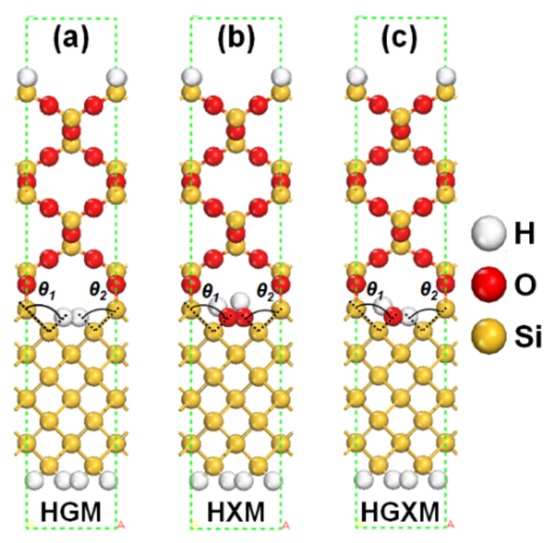
Atomic structures of the Si/SiO
2 interface. There are three different interfacial models formed by silica and silicon, namely the hydrogen model (HGM), hydroxyl model (HXM), and hydrogen-hydroxyl model (HGXM), as displayed in
Figure 5. Among the various possibilities of interfacial passivation [
37], we are interested only in the hydrogen atom (H) and hydroxyl group (OH), because the mainstream concept of previous studies for threshold degradation is the destruction of Si-OH bonds and Si-H bonds where the interaction between Si atom and -OH/-H is weak. The crystalline
β-cristobalite is adopted to represent the amorphous SiO
2 of oxidation process in all models, for which it has been found that the potential barrier heights of
β-cristobalite for electrons and holes are almost in accordance with that of amorphous silica [
37,
38]. More importantly, the lattice constant of
β-cristobalite is approximately
times that of diamond silicon [
39]; thus, the average mismatch of lattice constant is smaller than 6%. Furthermore, by means of introducing H atoms, the Si dangling-bonds at the top and bottom of the interfacial models are saturated to obtain the accurate and reliable results [
40]. The unit cell is an abrupt interfacial structure without a nominal transition region. We carry out the structural relaxation of the Si/SiO
2 interfacial models to reach the ground state of models and obtain the corresponding authentic parameters by depending on the aforementioned DFT method. The calculation results based on the lowest-energy conformation are listed in
Table 2. It can be found that the lengths of Si-H bonds and Si-OH bonds located between the Si layer and SiO
2 layer are 1.48 Å and 1.70 Å for HGM and HXM, respectively. In the case of HGXM, the bond lengths of Si-H and Si-OH are 1.47 Å and 1.68 Å, respectively, which are greatly close to that of HGM and HXM. However, there is a big difference between the angle of Si-Si-OH in the HXM; the
θ1 and
θ2 are 73.7° and 113.5°, respectively.
Density of states of the Si/SiO
2 interface. After determining the Si/SiO
2 interfacial configurations, we calculated their total and partial density of states (TDOS and PDOS) without and with electron irradiation to better understand the physical mechanism of threshold degradation at the atomic level. The TDOS and PDOS of HGM, HXM, and HGXM are presented in
Figure 5 and
Figure 6, respectively. One can find that there are some new electronic states in the energy band within the range of 0.0 eV to 0.7 eV after one H atom of HGM is removed, whereas for the HGM without H atoms the new electronic states are distributed in the range of 0.35 eV to 1.5 eV [see
Figure 6a]. This result manifests that the new states in the band gap are caused by Si atoms with dangling bonds. The PDOS of the HGM with one and two Si dangling-bands provides further evidence to the origin of new states. As presented in
Figure 6b, three new peaks of electronic states for the case of one Si dangling-band are observed and located at 0.06 eV, 0.32 eV, and 0.56 eV, respectively. There are four new peaks located above valence bands due to the fracture of two Si-H bonds; their energy coordinates are 0.48 eV, 0.60 eV, 0.80 eV, and 1.26 eV, respectively. For the scheme of passivation with OH group, it can be found that two new peaks are localized in the vicinity of the Fermi level when one of Si-OH bands is broken by high-energy electrons, while the TDOS of the HXM with two Si dangling bonds is almost similar with that of the HGM without H atoms [see
Figure 6c]. The result is further confirmed by the PDOS of the HXM with one and two Si dangling-bands, as illustrated in
Figure 6d. As can be seen, one new peak is generated in the valence bands and its energy coordinate is −0.25 eV; another two peaks are located above the valence bands at 0.09 eV and 0.42 eV for the case of one Si dangling bond, respectively. For the case of two Si dangling bonds, four new peaks are distributed in the conduction bands and the corresponding coordinates are almost the same as that of the HGM without H atoms. It is worth noting that the electronic states in the conduction bands are distinguished from those of the HXM with one Si dangling bond when the Si-H bond of HGXM is broken, as displayed in
Figure 6e,f. A weak peak at 0.39 eV is almost negligible, being five times smaller than the electronic-state peak induced by the Si dangling bond of the HXM. Nevertheless, the variation of electronic states in the conduction bands caused by the break of the Si-OH bond or Si-H/-OH bond after irradiating shows nearly no difference based on their TDOS and PDOS. These results clearly indicate that electron irradiation only affects the electronic states of the conduction bands in the HGM due to the fracture of Si-H bands, while for the HXM and HGXM, the electronic states near the Fermi level are changed on account of the existence of Si dangling bonds. Moreover, the variation of electronic states depends on the number of Si dangling bonds and the passivation scheme. In fact, the electronic states of conduction bands and valence bands (near the Fermi level) of the Si/SiO
2 interface will be simultaneously influenced in the practical engineering.
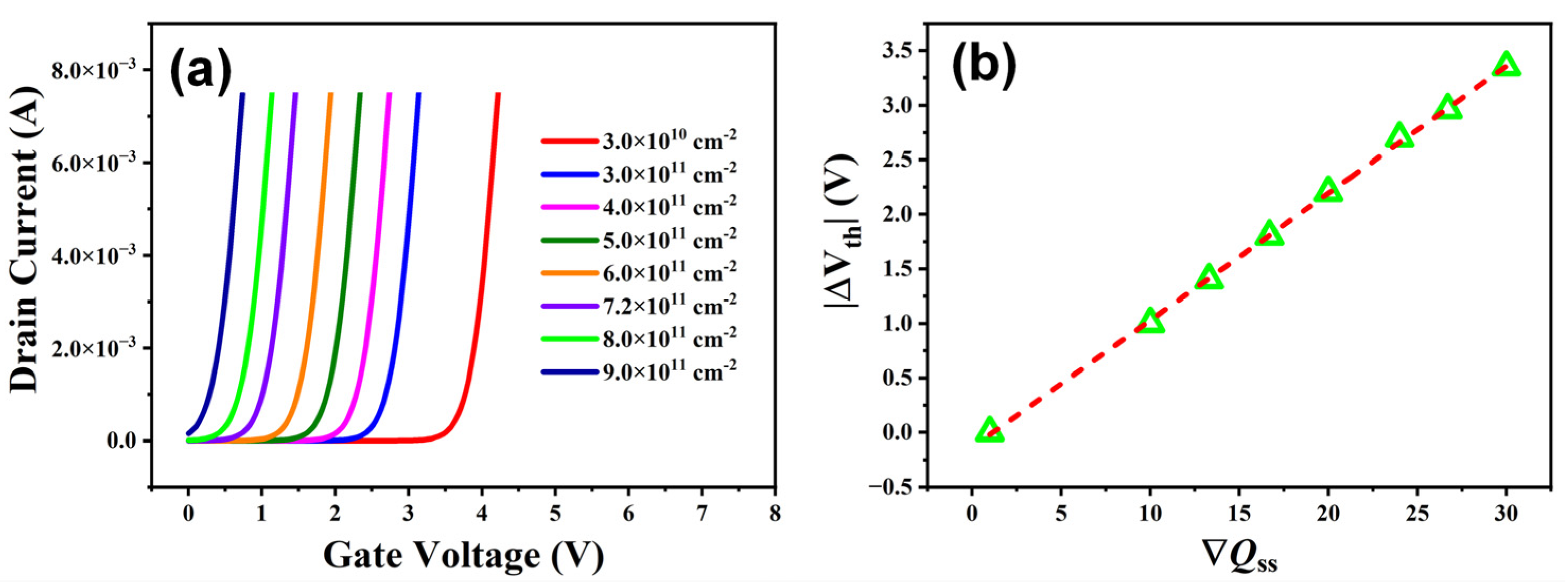
According to the above discussion, the diminution of V
th is ascribed to the increase in
Qss after irradiating. Therefore, to further explore the quantitative relationship between the ∇
Qss and ∆V
th, we carried out a TCAD simulation. Before starting the numerical simulation of the I
D–V
G of the irradiated devices, it is essential to validate the correctness and availability of the simulated model to acquire reasonable and reliable results.
Figure 7 clearly shows that the I
D-V
G curve of the simulated model is nearly in accordance with that of SJ-VDMOSFETs before irradiating, and the V
th of the simulated model with the
Qss of 3 × 10
10 cm
−2 is 3.5 V. These results authoritatively demonstrate the correctness and rationality of structural parameters of the simulated model. Afterwards, we determined the
Qss corresponding to the
D of 50 kGy is 7.2 × 10
11 cm
−2 according to the comparison of simulation result with experimental result. The simulated V
th for the
Qss of 7.2 × 10
11 cm
−2 is 0.80 V which is in good agreement with that of the irradiated device. The I
D-V
G curves of the simulated model with the
Qss of 3 × 10
10, 3 × 10
11, 4 × 10
11, 5 × 10
11, 6 × 10
11, 7.2 × 10
11, 8 × 10
11, and 9 × 10
11 cm
−2 are shown in
Figure 8a. It can be found that the I
D-V
G curve gradually shifts along the direction of decreasing gate voltage with the increase in
Qss, but the variation trend of the drain current with the increasing gate voltage is unchanged. The channel is almost open when the
Qss is up to 9 × 10
11 cm
−2, and the corresponding V
th is only 0.15 V; that is, 23 times smaller than the value with 3 × 10
10 cm
−2. The absolute value of ∆V
th (|∆V
th|) as a function of the ∇
Qss is illustrated in
Figure 8b. As a note, the
Qss of 3 × 10
10 cm
−2 and the V
th of 3.5 V are used as a benchmark for the change of
Qss and V
th, respectively. It is clearly shown that the |∆V
th| increases linearly with the increase in ∇
Qss and the increment between two |∆V
th| is 0.4 V in the range of 4 × 10
11 cm
−2 to 6 × 10
11 cm
−2 with a step of 1 × 10
11 cm
−2. The linear function obtained by fitting the scatter points is represented as |∆V
th| = 0.116∇
Qss − 0.137, where |∆V
th| = |V
th’ − 3.5| and ∇
Qss =
Qss’/(3 × 10
10). This formula clearly shows that the interface charge density is a critical factor for the reliability of gate oxide and the operation mode of MOS devices.


