1. Introduction
The recent development of NAND flash technology for high density has been extensively utilized in industry. The first vertical channel NAND flash technology was announced by Toshiba in 2007 [
1]. The Terabit Cell Array Transistor (TCAT) by Samsung [
2] and Stacked Memory Array Transistor (SMArT) by SK Hynix [
3] were developed in 2009 based on this structure. Since then, the development of vertical channel structures has grown rapidly. In particular, the layered stack of the vertical channel structure is expected to have a high-end structure of more than 200 layers in 2023 [
4,
5,
6].
Three-dimensional NAND memory is a high-density, cost-effective technology, but it still has some drawbacks, such as speed, cell size, and power consumption at the system level due to the required peripherals (e.g., charge pump). In particular, the program speed is pointed out as a weak point compared to other memories (ex: Dynamic Random Access Memory (DRAM)) in the NAND flash structure, and attempts to solve this have been studied.
To solve this problem, resistance change memory, such as Phase-Change Random Access Memory (PCRAM), Resistance Random Access Memory (RRAM), and Magnetic Random Access Memory (MRAM) are being actively studied as next-generation memory that can replace charge trap flash (CTF), which is currently used in 3D NAND flash memory. In particular, these resistance change memories have the advantage of relatively fast operating speed and low operating power [
6]. However, it is difficult to apply the resistance change memory to a large-scale product, especially when it is applied to the current 3D NAND flash structure, due to the disadvantage that only the one transistor-one resistor structure is possible compared to the CTF device that can be configured with one transistor.
As a result of this problem, most of the resistance-changing memories studied so far do not replace mass storage devices such as Solid-State Disks (SSD) and have limited use in specialized fields such as internal memory. Among these, in the case of ferroelectric memory recently studied using ferroelectric material [
7,
8,
9,
10], it is only necessary to replace the ONO structure used in the CTF flash with ferroelectric material. Therefore, the NAND flash structure using the ferroelectric memory basically has an advantage in that the existing NAND flash structure and operation method can be used as it is. Due to these strengths, research for applying ferroelectric memory to the 3D NAND structure, the latest structure of NAND flash, has progressed rapidly compared to other memory devices, and there are cases where actual devices have been made to prove the possibility [
11].
However, there are several problems in the practical application of ferroelectric memory to 3D NAND flash structures. Among them, the most urgent and major problem is the low operating speed of the Gate Induced Drain Leakage (GIDL) erasing method currently used in 3D NAND flash memory. In the early days of 3D NAND flash development, there was Bulk Erase of the TCAT structure and GIDL deletion of the Bit Cost Scalable (BiCS) structure, but as the structure of 3D NAND flash evolved to the COP structure to improve density, the peri circuit layer was placed underneath. Therefore, although it showed a faster erase speed compared to the GIDL erase method, the bulk erase method, which relies on the p+ sub-region under the string to supply hole carriers to supply the erase voltage to the channel, is deprecated. Therefore, although most of the currently manufactured 3D NAND flash structures use the GIDL erase method, this GIDL erase method has many disadvantages in actual operation because it requires making a hole carrier using the GIDL phenomenon. The biggest problem among them is that the operation speed is extremely slow.
Furthermore, if ferroelectric memory is applied to the 3D NAND flash structure, the GIDL erase method becomes a bigger problem because the operating voltage of the ferroelectric memory is very small compared to the operating voltage of the conventional CTF memory. Because it is the operating voltage that determines the GIDL erase speed, if the erase voltage is decreased to protect the performance of the ferroelectric memory and the ferroelectric film, the operation speed will inevitably be lowered. Therefore, in order to apply ferroelectric memory to the current 3D NAND flash structure, an innovative structure and operation method that can have a fast operation speed even at a low erase voltage is required. If this problem cannot be solved, even if ferroelectric memory is applied to the 3D NAND flash structure, the program speed will only be faster, and the erase speed will be slower than the existing CTF memory. To address this, this paper proposes and validates a Silicon-Pillar (SP) structure capable of supplying high-speed hall carriers by columns inside the 3D NAND flash string.
2. Details of the Proposed Structures
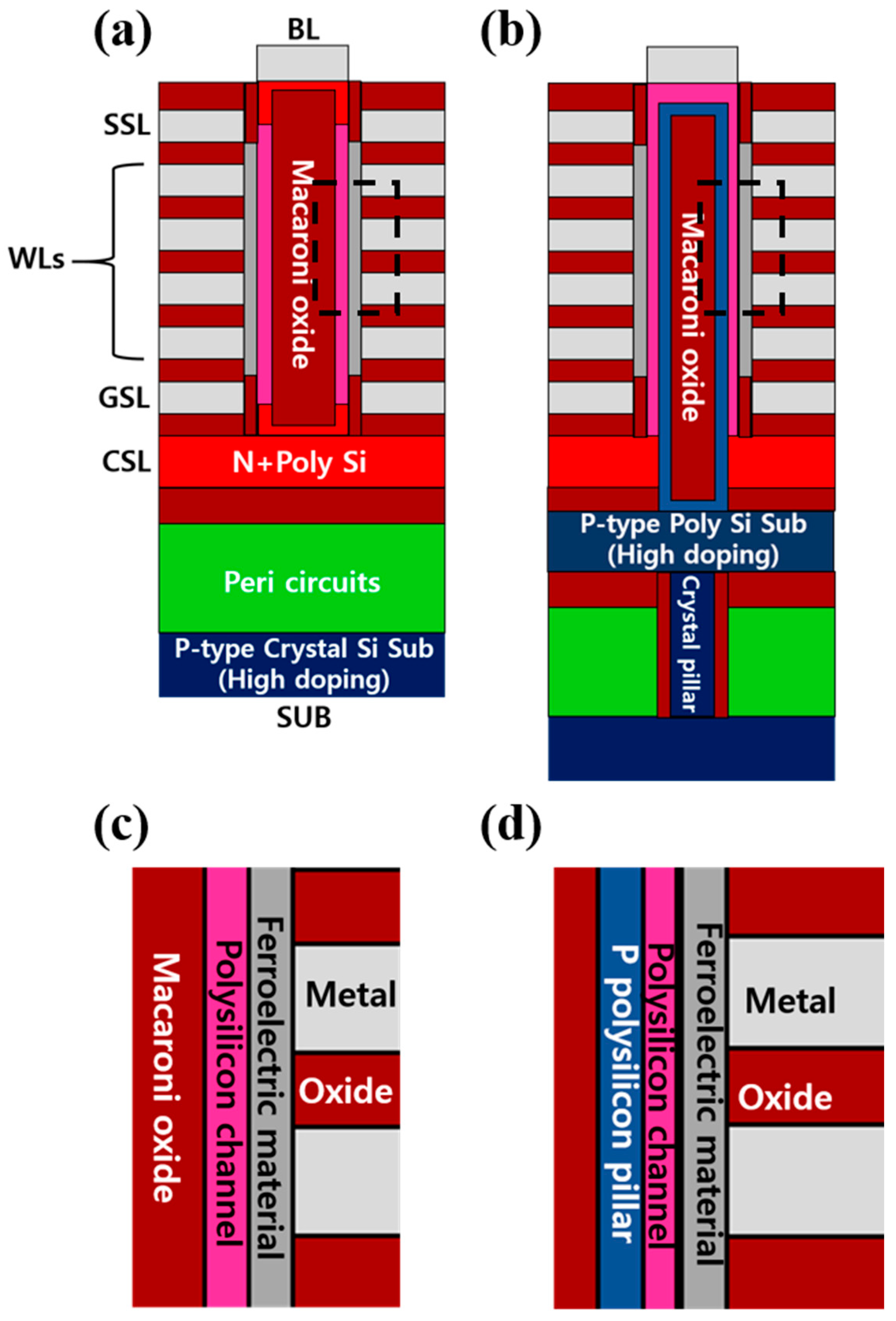
Figure 1 describes the structure proposed in this study by comparing it with the general 3D NAND flash structure. First, it is assumed that a ferroelectric memory is applied to the general 3D NAND flash structure described in (a) and (c). In this structure, the lower P+ crystal sub-region is completely separated from the single memory string and simply plays the role of a substrate for the Peri circuit. Therefore, the supply of hole carriers to increase the channel voltage in the erase operation depends entirely on the GIDL phenomenon that occurs in the N+ doping region (red color) of the GSL and SSL transistor regions. Therefore, in this structure, the erase speed will take about 1.5 ms [
12] only for the rise of the channel voltage, so the fast operation speed of the ferroelectric memory will not be reflected at all and will operate very slowly.
Next, the SP structure described in (b) and (d) is based on the IP structure presented in a previous study [
13]. As shown in (b), the proposed SP structure can serve as a passageway for hole carriers rich in crystal pillars connected in the P+ polysilicon sub-region to move upward, unlike the existing 3D NAND flash structure. Next, the P+ polysilicon sub-region on the upper part of the Peri circuits exists to stably supply the holes supplied from the crystal pillar to the upper P polysilicon pillar. Of course, it is ideal that the lower crystal pillar and the upper polysilicon pillar are directly connected one to one. However, in reality, it is almost impossible to align pillars with a diameter of only several tens of nanometers through lithography. Therefore, in order to secure the degree of freedom, an additional sub-region with a large area is absolutely necessary. In the figure, for convenience, the upper polysilicon pillar and the lower crystal silicon pillar are located at the same location, but in the actual structure, they can be freely placed at any position in the P+ polysilicon sub-region.
The supplied hole carriers are quickly supplied to the adjacent intrinsic polysilicon channel on the P polysilicon pillar, and at the same time, the high erase voltage applied from the BL contact and the CSL contact can be transmitted to the channel. Because the expected performance of the proposed SP structure, especially the rising rate of the channel voltage, has already been confirmed in the IP structure published by our previous study, using this structure can improve the very slow erase speed of the existing 3D NAND flash structure. Due to these advantages, the proposed SP structure will become a new structure that can properly utilize the speed of ferroelectric memory in the 3D NAND flash structure.
3. Simulation Results and Discussion
3.1. Simulated Structures, Models, and Parameters
In this paper, Synopsys’ Sentaurus TCAD tool [
14] was used. The structure editor tool was used to design the proposed structure in
Figure 2 above. This structure was used as a Virtual Gate All (GAA) structure during device simulation via the Sentaurus tool’s cylindrical command (Rotate 360 degrees). Next, in the composition of each contact, starting with the SUB contact at the bottom, the Common-Source-Line (CSL) contact serves a ground function, and the Ground-Select-Line (GSL) located above it controls a total of 10 word lines (WLs), and the Source-Select-Line (SSL) contact serves as a gate for control Bit-Line(BL). Finally, the uppermost Bit-Line (BL) serves as a drain.
Figure 2b shows an expanded view of the dimensions of the elements used in the simulated device. The Macaroni(M)oxide, pillar, channel, and ferroelectric layer thicknesses were held at 0~20, 30~10, 10, and 10 nm, respectively. Therefore, the total diameter of the simulation device is 100 nm. The word line gate length and the interval between successive word lines were fixed at 30 nm. It is also confirmed that the doping concentration dependence, high field saturation, and trap scattering mobility models were used in the given device simulations. In addition, Shockley–Read–Hall [
15], Auger [
16], and Hurkx band-to-band recombination models [
17] were also used to simulate the operation of the transistor in a 3D NAND flash structure.
Figure 3 shows the doping concentration of the formed structure and additional information on the SSL, GSL, and SUB-regions. First, in the case of the SSL region shown in (b), the length of the SSL gate is set to 100 nm, and this is also the case for the GSL in (c). This is for suppression of leakage current flowing to BL and CSL, respectively, and enhancement of gate control capability. It is known that such a structure or a plurality of gates is used in the actual 3D NAND structure. Second, the doping concentration of the pillar was set to a lower concentration (5 × 10
18 cm
−3) than that of the lower sub-region. This is in consideration of the difficulties in the process and the change of the threshold voltage due to the increase in the doping concentration. Lastly, the position of the crystal pillar in the sub-region is the same as the upper polysilicon pillar for the convenience of simulation. However, in reality, it will be placed at the optimal position considering the area and performance of the Peri circuits. In addition, the following document [
13] was referred to for the selection of the parameters for reflecting the trap characteristics of the polysilicon channel. Finally, among the ferroelectric parameters of the ferroelectric, the Saturation polarization (P
s) was set to 30 uC/cm
2, the Remanent polarization (P
r) was set to 25 uC/cm
2, and the Coercive field (E
c) was set to 2 MV/cm. Additionally, the Time for the polarization was set to 0 s. This setting is too ideal, but in this paper, we want to confirm that the operation of ferroelectric memory can be effectively implemented in existing 3D NAND flash structures, so reliability such as retention and endurance is not considered, and the reliability part is to be confirmed by fabricating actual devices in the next study.
3.2. Analysis of the Erase Speed of Ferroelectric Memory When GIDL Erase Is Used
In this paper, we first analyzed the operation speed, especially the erase speed, when using a ferroelectric memory in a structure using general GIDL erase. In particular, since the ferroelectric memory operates at a lower voltage compared to the existing CTF memory due to its characteristics, it is very important to check the operating speed reflecting this low voltage.
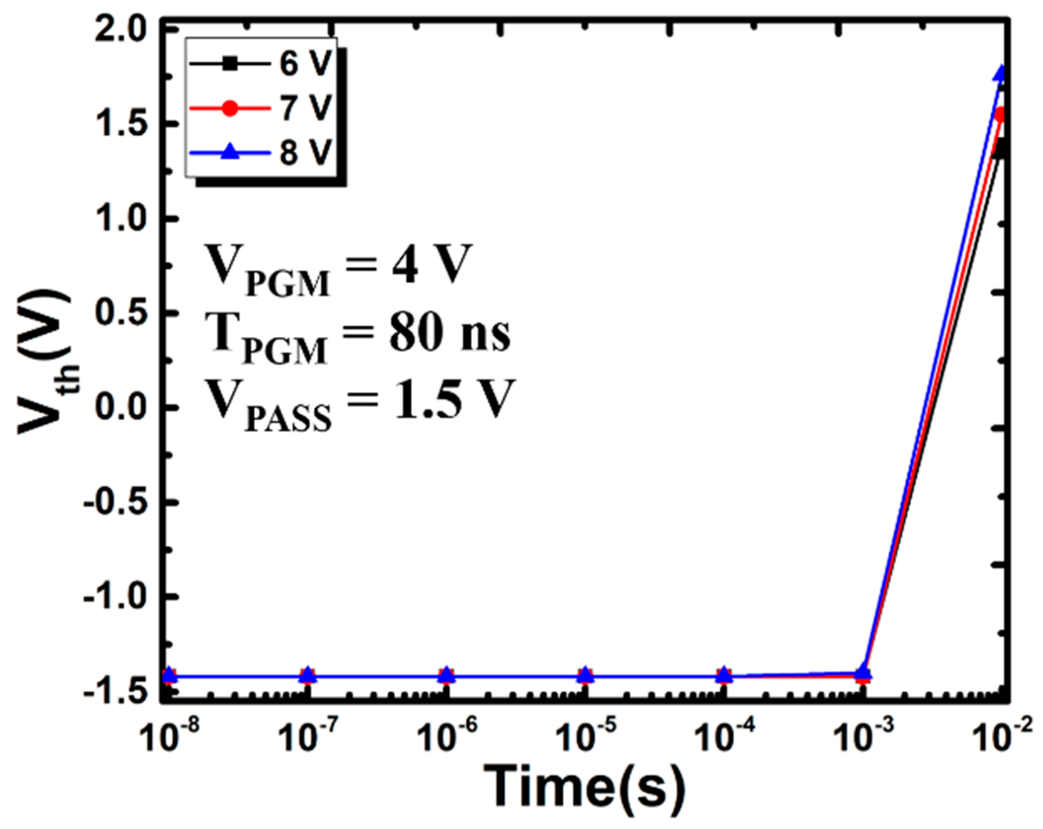
Figure 4 is the result of verifying the erase speed in the GIDL erase structure composed of 10 WLs while having the same geometry as the SP structure described above. First, as shown in T
PGM in
Figure 4, the program operation that directly applies a voltage to the gate proceeds at a high speed of 80 ns. However, on the contrary, the erase operation that needs to increase the channel voltage due to the channel GIDL phenomenon does not progress at all until 1 ms, and it can be seen that the erasing operation completely proceeds after 10 ms. In particular, the fact that the erase voltage does not increase at all, even when the erase voltage is increased to 8 V, suggests that it is impossible to improve the erase speed by simply increasing the erase voltage.
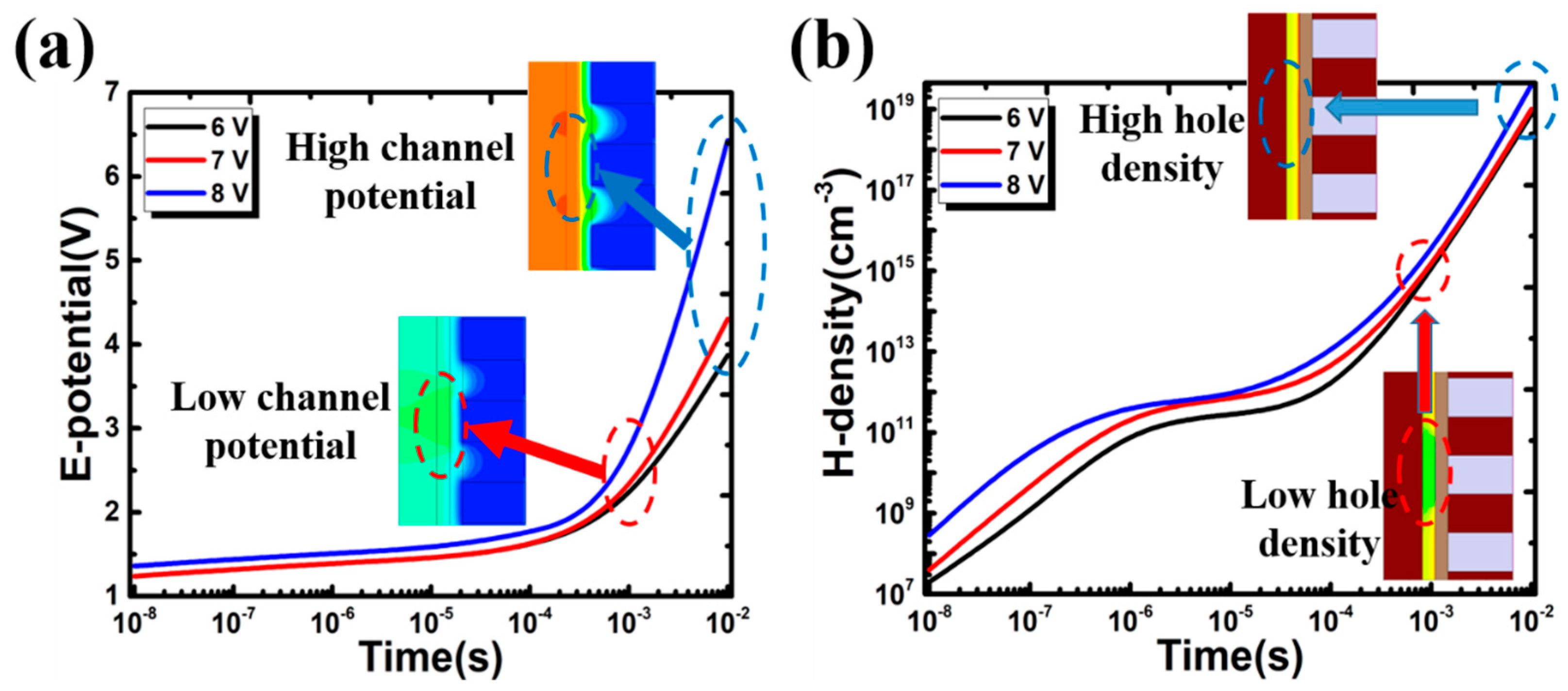
The cause of the slow speed of the erase operation identified in
Figure 4 can be explained in
Figure 5. First, looking at the change in channel potential through (a), it can be seen that the channel potential rose only 2.2~3 V when the erase operation time progressed to 1 ms. Of course, in this voltage range, E
c (2.5 MV/cm), one of the ferroelectric parameters set for this simulation, is not satisfied, or the erase operation will not proceed because it has a value that is almost meaningless. In fact, a time point at which a channel potential rises to a level at which an erase operation may proceed is 10 ms, and in this case, the channel potential rises to 3.5 to 6.2 V according to a change in an operating voltage (6 to 8 V), and this voltage range greatly exceeds the aforementioned Ec, and thus an erase operation can be performed. Next, looking at the change in the hole carrier density of the channel in the same time zone through (b), it can be seen that it is also very low at about 10
15 cm
−3 at the time of 1 ms. With this degree of hole carrier density, it is natural that the erase voltage (6 to 8 V) applied in the BL and CSL contact is not transferred to the channel properly, and this problem may be seen when the normal erase operation is performed only when the hole carrier density exceeds 10
19 cm
−3 at a time of 10 ms.
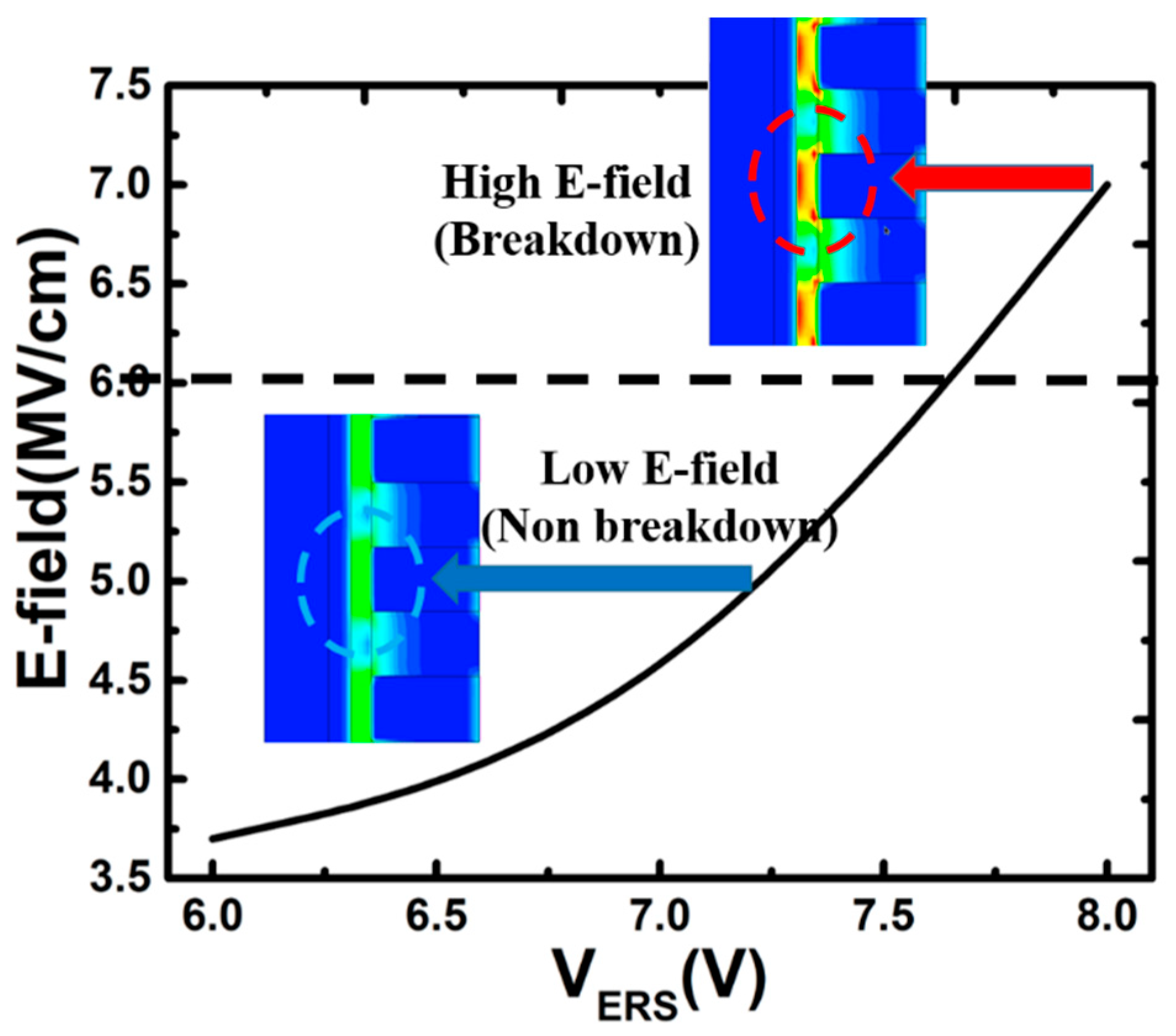
From the above results, it may be seen that the change in the hole carrier density does not show a significant change more than when the voltage exceeds a predetermined value (1019 cm−3), but the change in the channel potential gradually increases. Therefore, in order to shorten the operation time, an operation voltage close to 20 V, which is an erase operation voltage of CTF memory, may also be considered. (Of course, in the erase operation, the reduction in power consumption due to the low operating voltage, which is an advantage of ferroelectric memory, should be given up.) However, recklessly increasing the erase operating voltage can be very dangerous. This is because the thickness of the CTF memory layer currently used is about 20 nm, but the thickness of the ferroelectric memory layer is being studied to be about 10 nm, and the breakdown limit of the ferroelectric material itself is known to be only 6 MV/cm.
As can be seen in
Figure 6, the increase in operating voltage sharply increases the E-field and increases stress applied to the ferroelectric thin film, thus increasing the breakdown potential. Until now, various research results have been published on the breakdown of ferroelectric thin films with ferroelectric properties, but assuming 6 MV/cm, which is the breakdown field of a typical ferroelectric thin film [
18], the maximum erase operation voltage that can be applied at a thickness of 10 nm is 7.6 V. Of course, assuming a very ideal situation, in order to avoid the possibility of a breakdown of the ferroelectric thin film, it is possible to think of a method of quickly generating hole carriers with a high erase voltage and reducing the erase voltage at the moment when the hole carriers are sufficiently filled in the channel. However, in an actual device, the speed at which the hole carrier is charged and the speed at which the channel voltage is increased may vary for each string by the influence of traps and other defects randomly present on the polysilicon channel or the surface. In addition, it is clear that there will be a difference in the transmission speed of the operation signal in a large-scale string currently used, and even if the difference is only several ns, the breakdown of the ferroelectric layer by high voltage is sufficient. Accordingly, in order to overcome this problem, a structure and an operation method for quickly supplying hole carriers to the channel even with a low operating voltage are required. If this structure and operation method can be secured, the ferroelectric memory can be applied to the 3D NAND structure to catch two rabbits at once: fast operation speed and high integration of the 3D NAND flash structure.
3.3. Analysis of the Erase Speed of Ferroelectric Memory When the Proposed Structure Is Used
In this section, we will check the performance and considerations of the proposed SP structure as a new concept structure mentioned above.
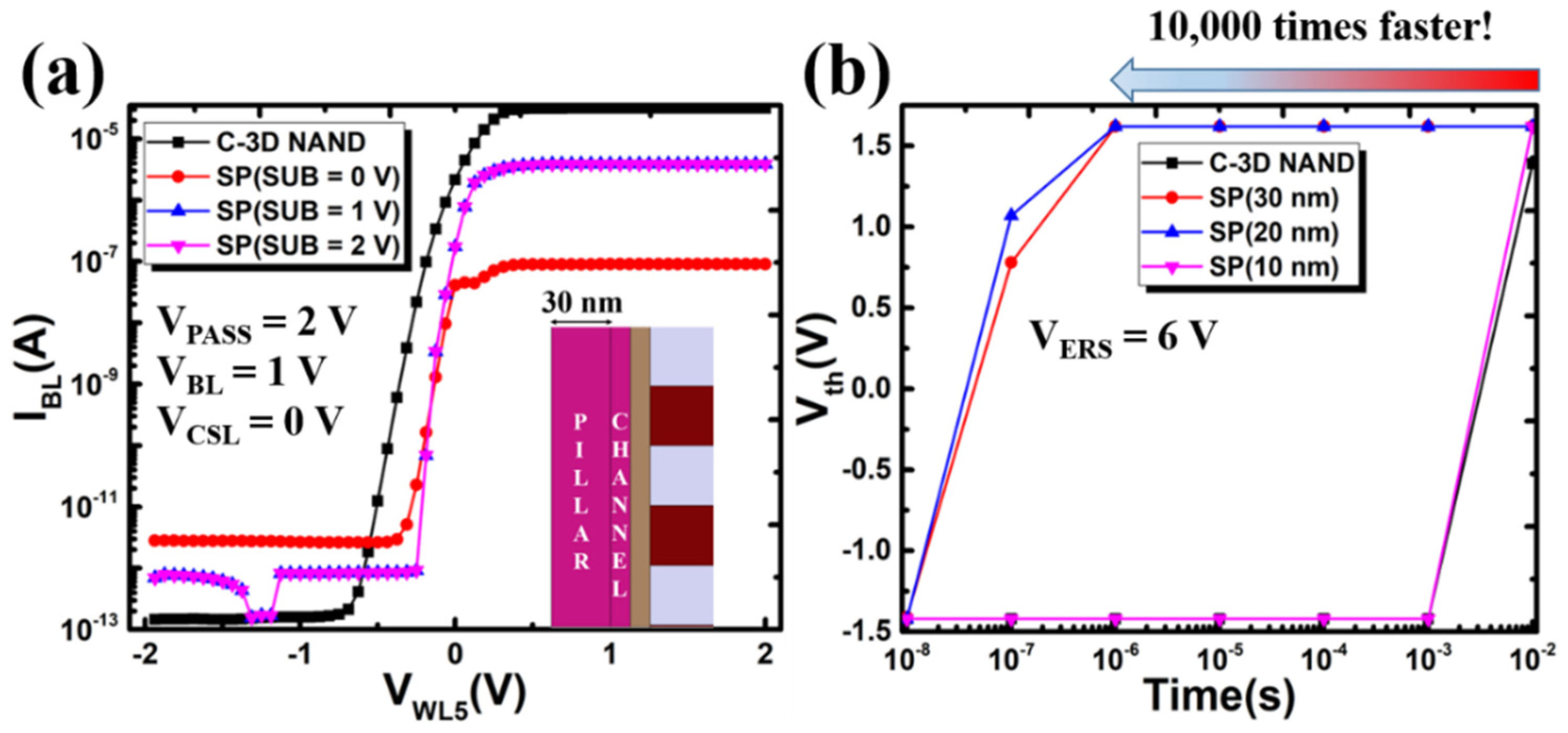
As seen in
Figure 7a, the leakage current generated in the SP structure is about 10
−12 A, which is one order higher than that of the general 3D NAND structure. However, this leakage current can be suppressed by increasing the voltage of the SUB and increasing the potential of the SUB. Instead, what was additionally confirmed was band bending caused by the P-type pillar and the lowering of the operating current due to the disturbance of electrons. This problem can also be solved by increasing the voltage (0 ->2 V) of the SUB contact. Additionally, it can be seen that the voltage rise of the pillar through the SUB contact greatly improves the Subthreshold Swing (SS) of the I-V curve (200 mV/dec -> 86 mV/dec). Unlike the general 3D NAND structure in which the SUB contact cannot exist, the SP structure in which the potential of the entire channel can be kept constant by the pillars shows that a much more stable operation is possible. For this reason, it is shown that the stability in Multi Level Cell (MLC) operation, which is essential for current NAND flash operation, can also be greatly improved. Next, as shown in
Figure 7b, the erase performance of the proposed SP structure is very good, and in particular, in terms of erase speed, it can be confirmed that it shows a speed more than 10,000 times faster than that of the GIDL erase method. However, as expected, the erase speed decreases as the thickness of the pillar decreases. In particular, when the thickness is 10 nm, it can be seen that the same speed as the GIDL erase method is shown except for a slight increase in the memory window (0.23 V).
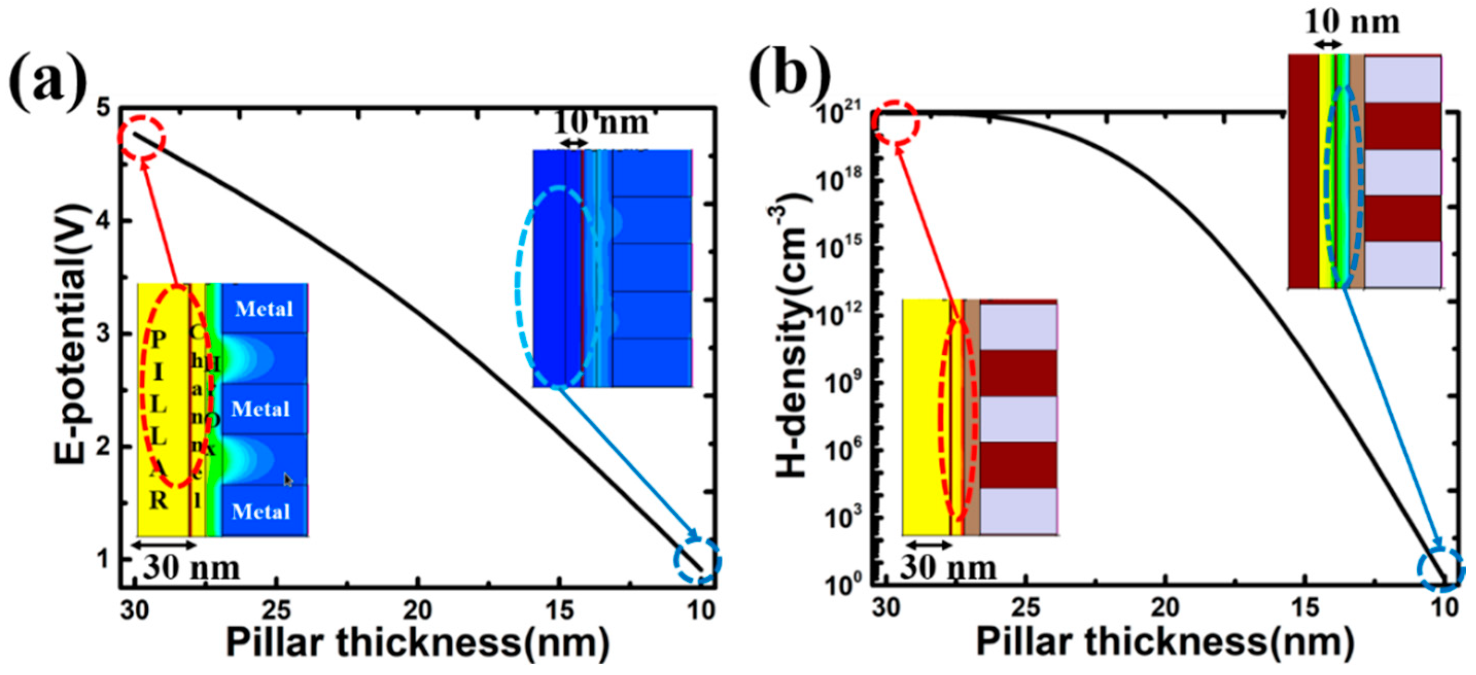
Figure 8 explains the difference in the erasing speed according to the change in the thickness of the column, as in
Figure 7. As expected, it can be seen that the channel potential and hole density rapidly decrease as the thickness of the column decreases. This phenomenon can be said to be because the supply of hole carriers is not smooth due to the decrease in the thickness of the pillar. In particular, when the thickness of the pillar is 10 nm, the channel potential rises by only 0.91 V, and the density of the hole carriers is also close to zero. For this reason, as in the previous results, there is almost no difference between the erase operation speed and the existing GIDL erase operation, and so real erase operation is thought to depend on the GIDL phenomenon, which is operated much later without the supply of hole carriers by the pillar. Therefore, in order to secure a stable erasing operation speed, it is preferable that the thickness of the pillar is 20 nm or more, but it is difficult for the reasons described below. In terms of the actual device, if the pillar thickness is designed to be 30 nm, there is virtually no space for the M-Oxide to be located. This point is practically difficult to use because it gives up the grain boundary suppression function of the polysilicon channel, which is an important function of M-oxide, and it can be said that the structure from 20 nm is realistic. Furthermore, in order to form a more stable polysilicon channel, it is also desirable to increase the thickness of the M-oxide, so it is necessary to enable fast operation even when the thickness of the pillar is 10 nm or less.
3.4. Two-Step Erase Method to Achieve Fast Erase Operation on Structures with a Pillar Thickness of 10 nm or Less
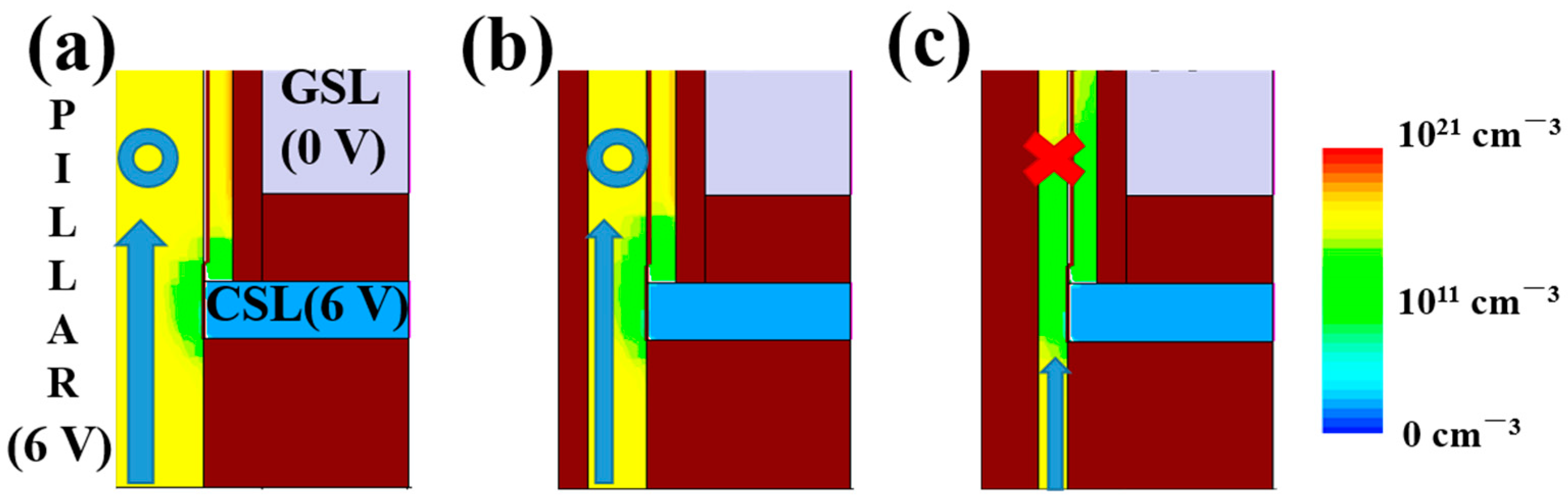
Figure 9 shows the change in hole density in the CSL region, which is the cause of the change in hole density according to the change in the thickness of the pillar shown in
Figure 8. When the voltage of the pillar and the voltage of the CSL contact are equal to 6 V, it can be seen that the voltage of the CSL prevents the flow of hole carriers moving through the pillar. However, when the thickness of the pillar is sufficiently thick (30~20 nm), since there is a region not affected by the CSL voltage, hole carriers move through the region to supply the hole carriers to the channel. Conversely, when the thickness of the pillar is thin (10 nm), since the CSL voltage affects the entire pillar, the hole carriers cannot move and are trapped, which prevents the hole carriers from being supplied to the channel.
Therefore, in order to solve this problem, it is necessary to use a two-step erase method that does not interfere with the movement of hole carriers by appropriately adjusting the CSL voltage.
In the proposed two-step deletion method, as shown in
Figure 10, the voltage of the BL contact and the CSL contact is set to Hole Charging Voltage (V
hc) lower than Erase voltage (V
erase) during the Hole Charging Time1 (T
hc1), and through this, the pillar and channel are charged with hole carriers. The Hole Charging Time2 (T
hc2) of the two contacts is properly adjusted so that the hole carrier can be fully transmitted to the channel. With this method, it is possible to sufficiently supply hole carriers to the channel even with a thin pillar.
Figure 10c shows the results of comparing the erase performance according to the difference in T
hc2 when the two-step erase method is used in the SP structure using a pillar with a thickness of 10 nm. Interestingly, when T
hc2 is 100 ns, the erase speed does not show much difference from the result of the GIDL erase operation but increasing T
hc2 by 1 us dramatically increases performance.
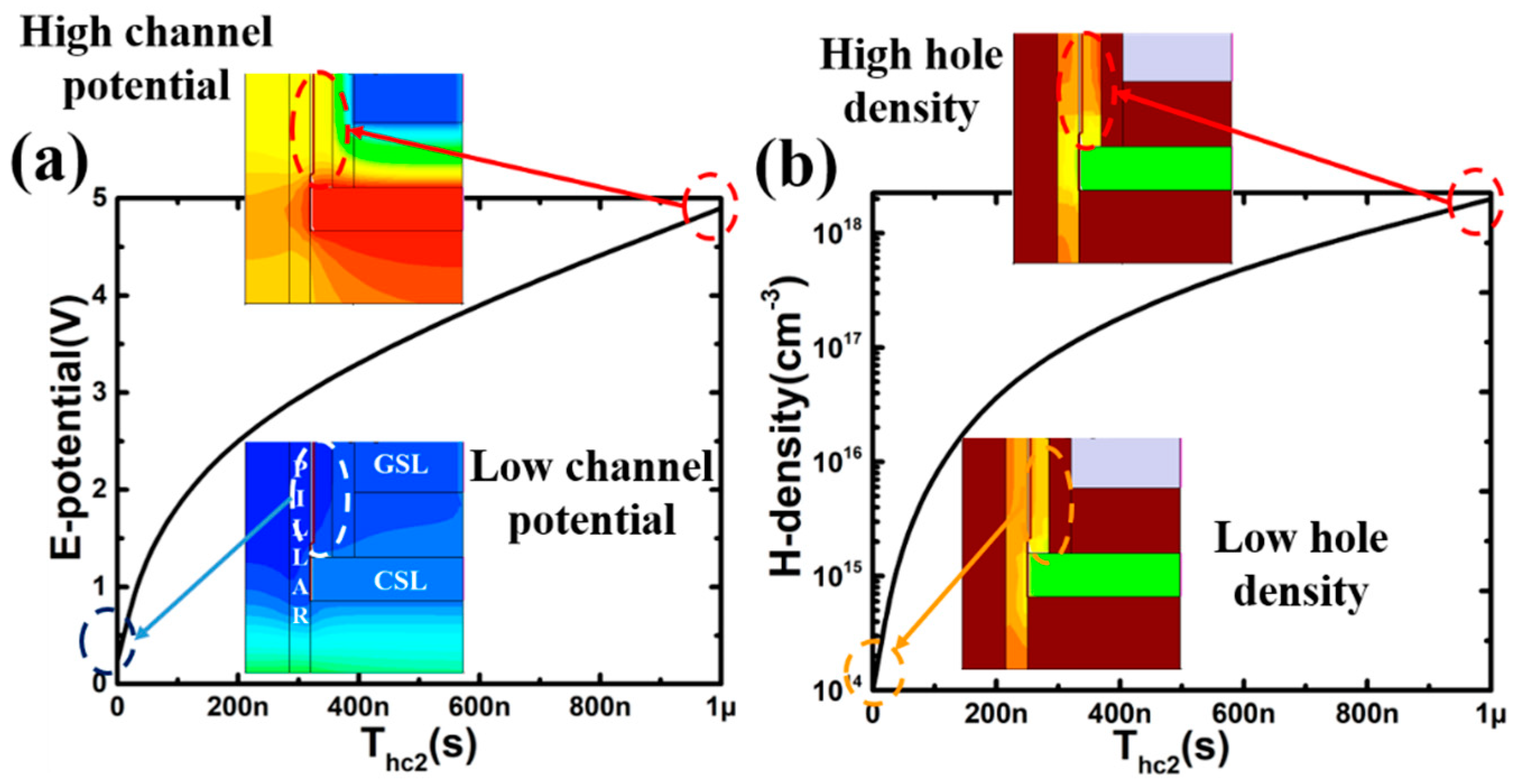
Figure 11 explains how the difference in erase speed of
Figure 10c occurs. First, in the T
hc1 section, the voltage of the CSL and BL contact points is 0 V, and only the SUB voltage is 6 V, so the hole carrier can move quickly through the pillar. The problem is that the T
hc2 section raises the voltage between the CSL contact and the B contact. If this section is short (100 ns), as shown in (a)-Low channel potential, the hole carriers in the channel are not sufficiently filled due to the rapidly rising CSL voltage. In this state, the supply of hole carriers through the pillar and the change in potential are blocked. Therefore, it can be seen that the CSL contact and the channel region with sufficient hole carriers are far apart, as shown (b)-Low hole density. However, if the time of T
hc2 is increased to 1us, the distance between the CSL contact point and the point where the hole carriers are sufficient is reduced, as shown (b)-High hole density because the hole carrier supplied through the pillar has enough time to fill the channel. Therefore, finally, the change in the potential of the channel rises from 2.71 V to 4.9 V, and the erase speed also rises sharply accordingly. In conclusion, it was confirmed that even if the thickness of the pillar becomes 10 nm, the proposed structure can show an erase speed of 1 μs if the operation method is properly controlled.
4. Conclusions
In this paper, the SP structure, a new structure to improve the erase speed in the 3D NAND flash structure to which ferroelectric memory is applied, was proposed and verified. First, it was confirmed that when the GIDL erase method used in the 3D NAND structure using the existing CTF memory is applied as it is, the operation speed takes more than 10 ms for various reasons. Next, as a result of using the SP structure to solve this problem, even if the existing erase method was used until the thickness of the pillar was 20 nm, a fast erase speed of 1us was achieved thanks to the hole carriers rapidly supplied through the pillar. Next, when the thickness of the pillar is 10 nm, the erase operation time is greatly delayed by the existing erase method, but when the two-step method is used, the hole carrier is sufficiently supplied to the channel, and the erase operation time is maintained at 1 μs. In conclusion, it is confirmed that the application of the proposed SP structure maximizes the fast operating performance of ferroelectric memory and secures the biggest advantage of the 3D NAND flash structure, the degree of integration.


