
The Impact of an Extended Gate Field Plate on the DC and RF Characteristics of a Junctionless Thin-Film Transistor


Abstract
:1. Introduction
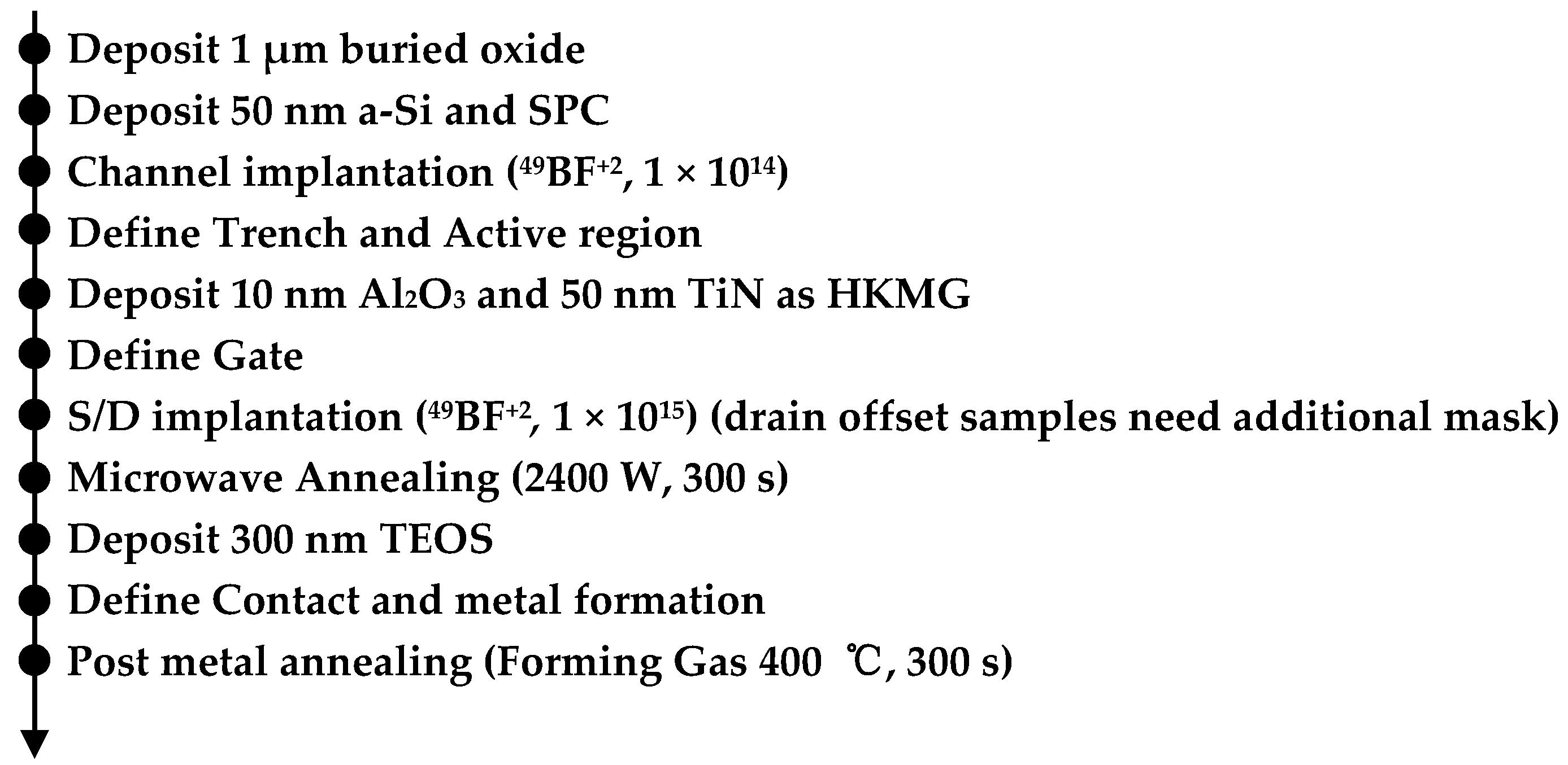
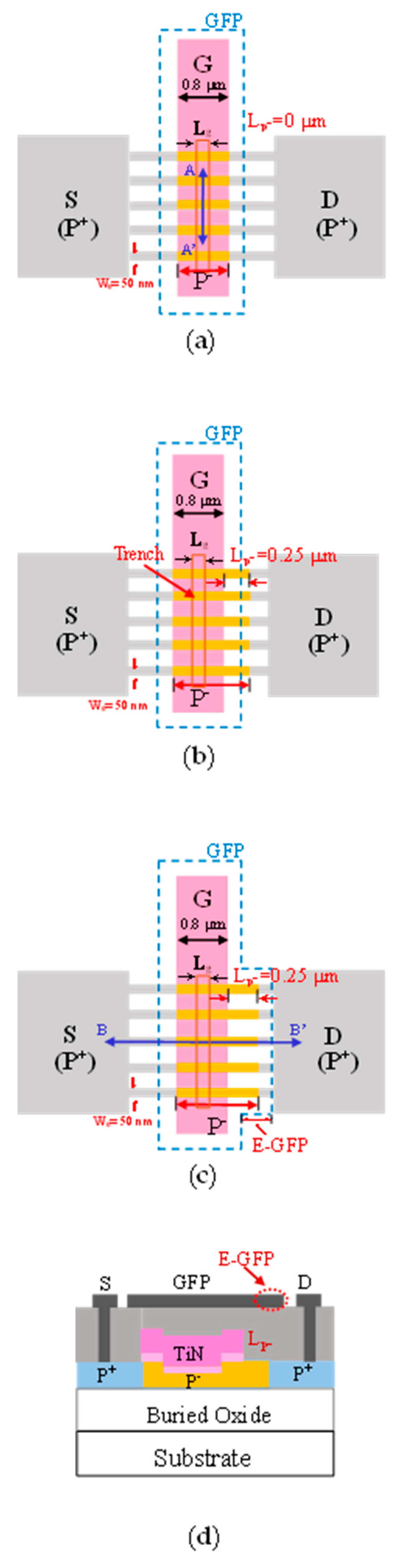
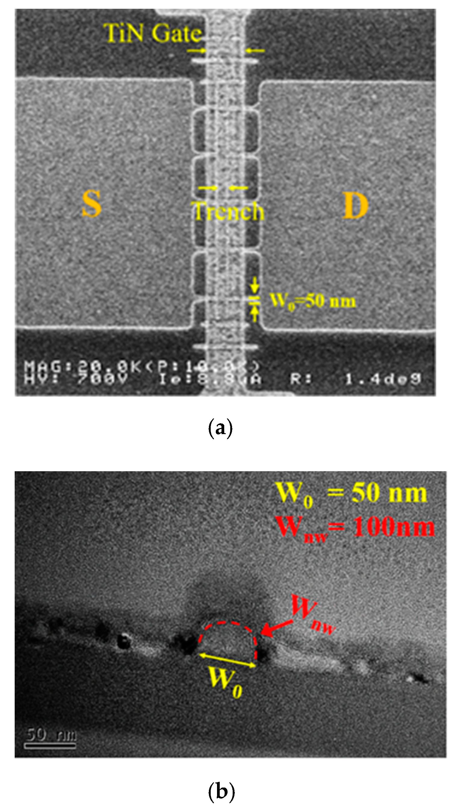
2. Experiments
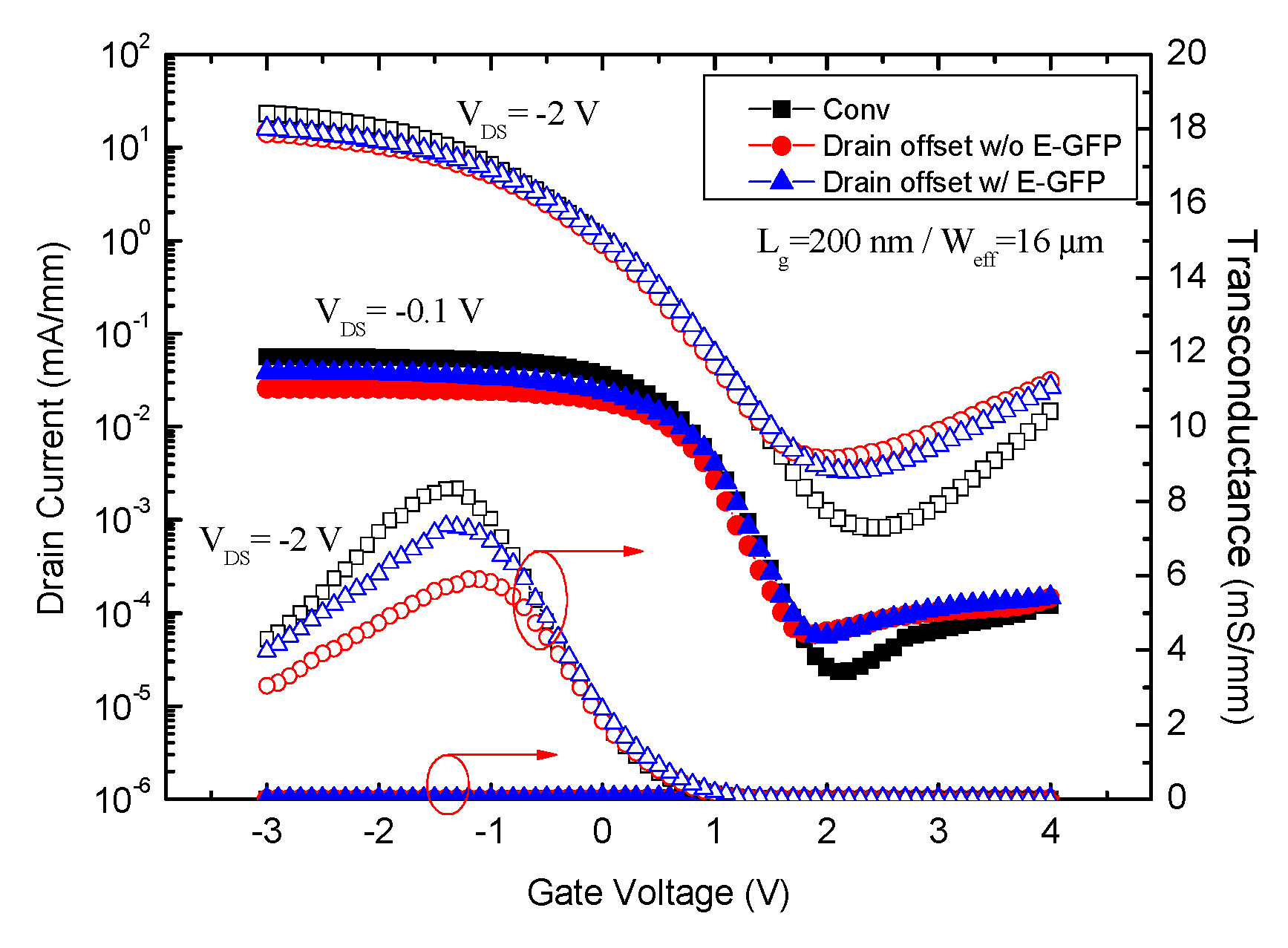
3. Results
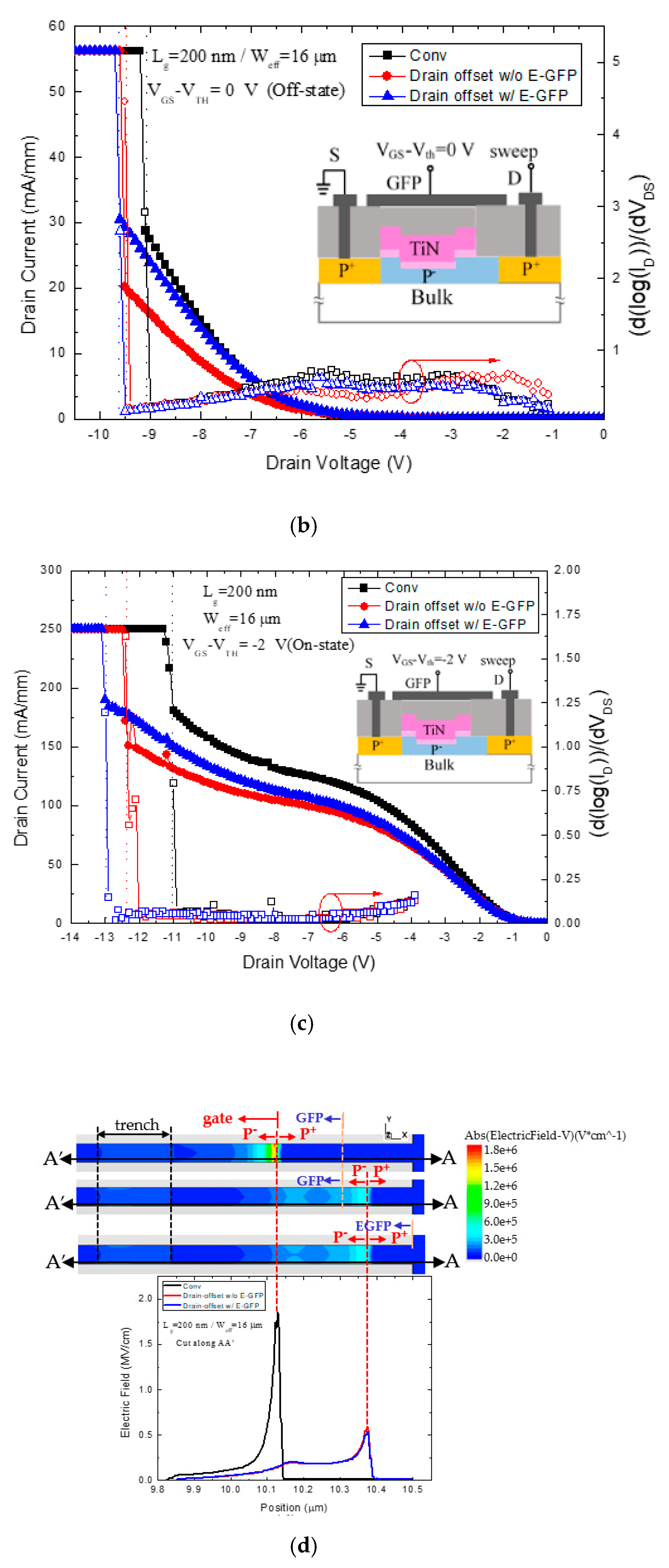
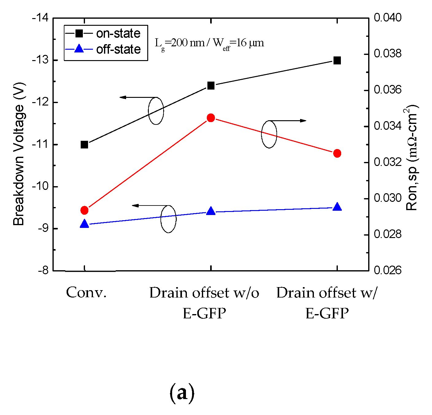
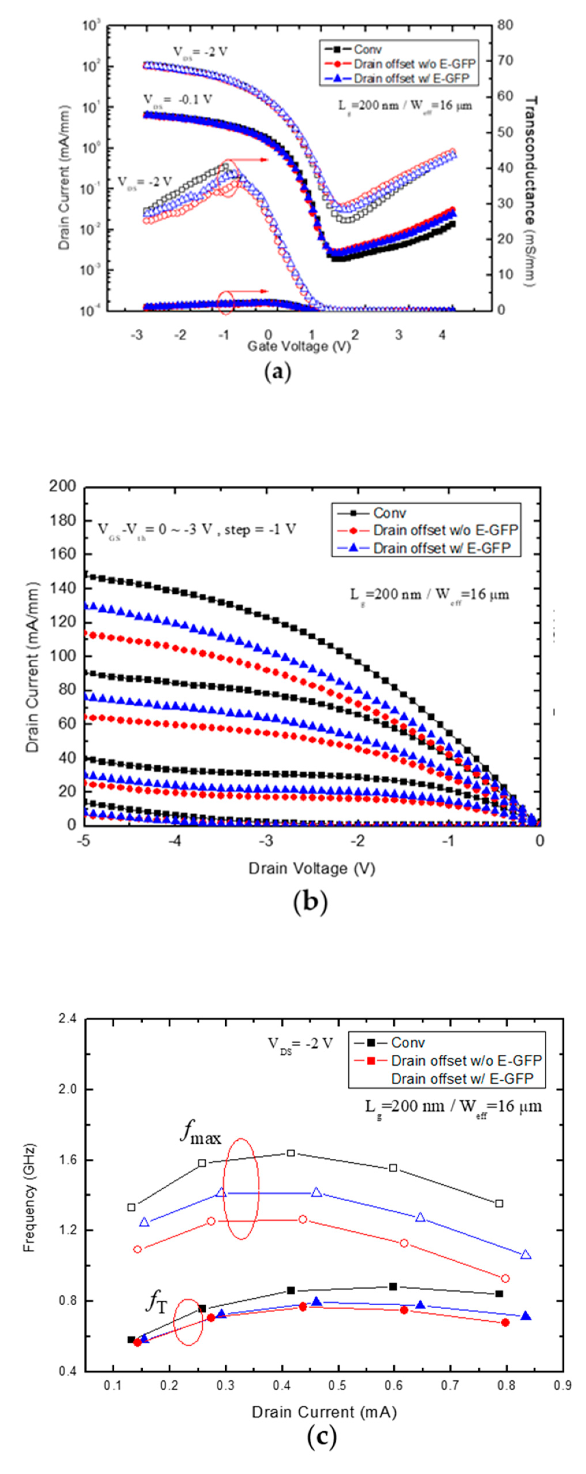
3.1. DC and Breakdown Characteristics
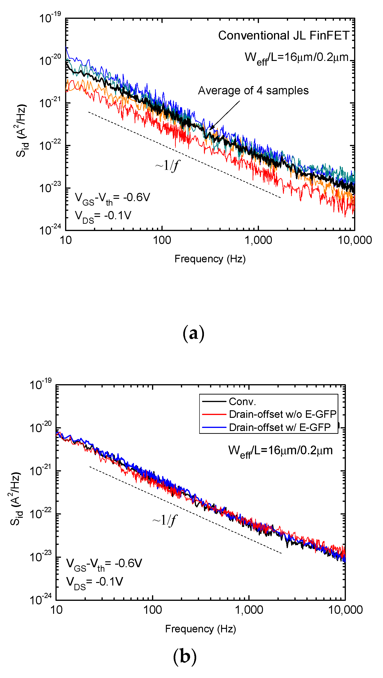
3.2. Low-Frequency Noise Characteristics
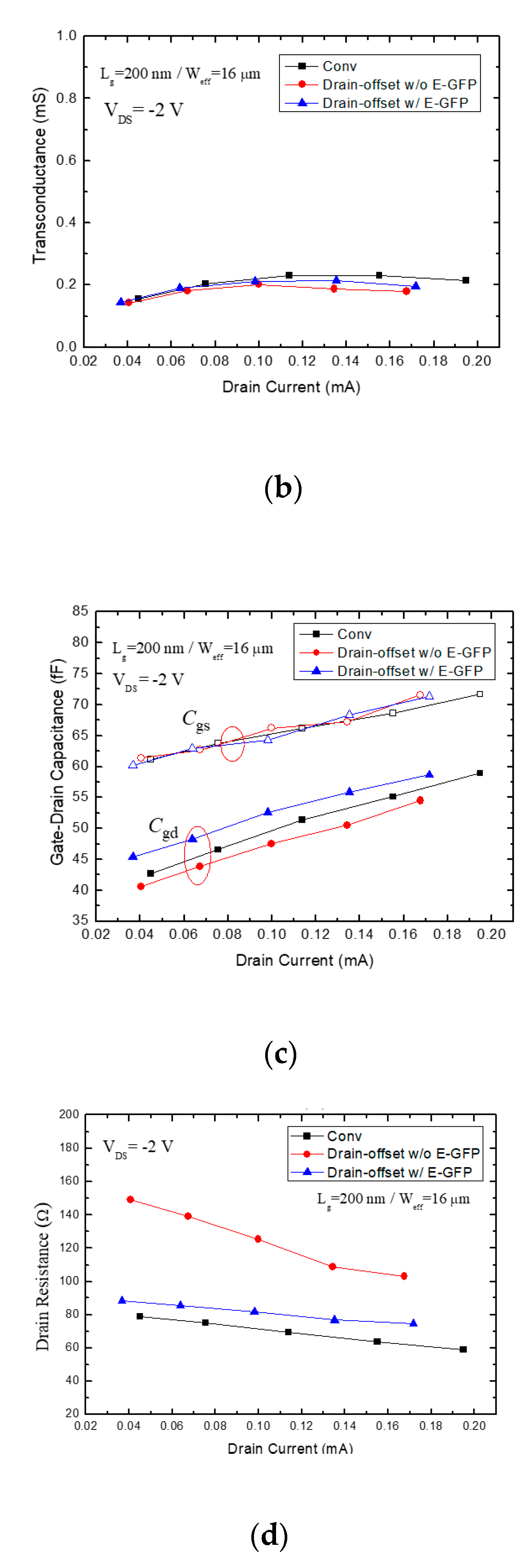
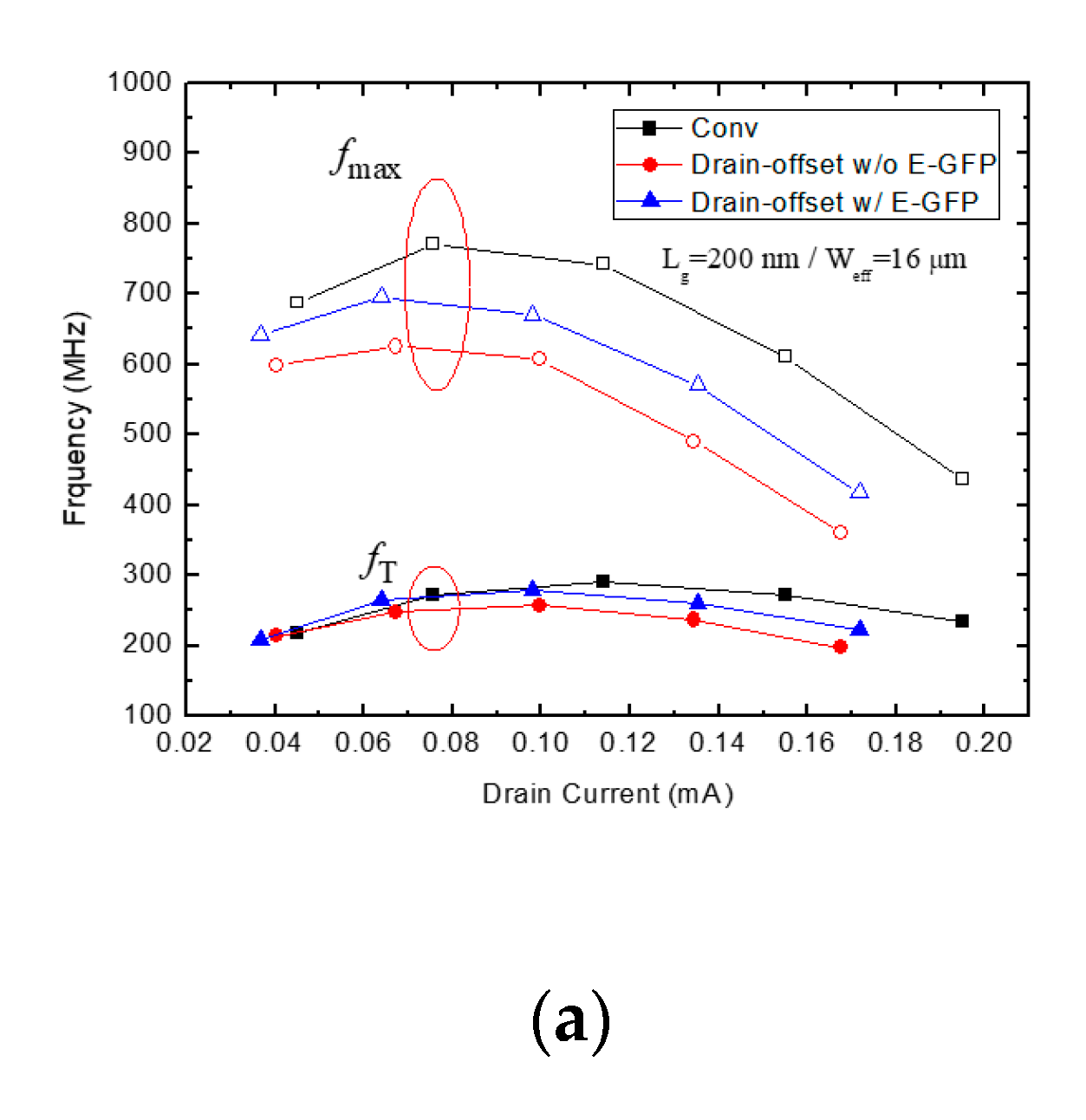
3.3. AC Characteristics
3.4. Postmetal Annealing (PMA)
4. Conclusions
Author Contributions
Funding
Acknowledgments
Conflicts of Interest
References
- Botrel, J.; Savry, O.; Rozeau, O.; Templier, F.; Jomaah, J. Polysilicon high frequency devices for large area electronics: Characterization, simulation and modeling. Thin Solid Film. 2007, 515, 7422–7427. [Google Scholar] [CrossRef]
- Chen, Y.-J.E.; Lee, Y.-J.; Yu, Y.-H. Investigation of Polysilicon Thin-Film Transistor Technology for RF Applications. IEEE Trans. Microw. Theory Tech. 2010, 58, 2076911. [Google Scholar] [CrossRef]
- Kim, S.Y.; Loke, W.-F.; Jung, B.; Roy, K. High-Frequency Modeling of Poly-Si Thin-Film Transistors for Low-Cost RF Applications. IEEE Trans. Electron Devices 2012, 59, 2296–2301. [Google Scholar] [CrossRef]
- Yu, Y.-H.; Chen, Y.-J.E. Ring-Based Direct Injection-Locked Frequency Divider in Display Technology. IEEE Microw. Wirel. Components Lett. 2008, 18, 752–754. [Google Scholar] [CrossRef]
- Lin, W.M.; Liu, S.I.; Kuo, C.H.; Li, C.H.; Hsieh, Y.J.; Liu, C.T. A phase-locked loop with self-calibrated charge Pumps in 3-μm LTPS-TFT Technology. IEEE Trans. Circuits Syst. II Express Briefs 2009, 56, 142–146. [Google Scholar]
- Yu, Y.-H.; Lee, Y.-J.; Li, Y.-H.; Kuo, C.-H.; Li, C.-H.; Hsieh, Y.-J.; Liu, C.-T.; Chen, Y.-J. An LTPS TFT Demodulator for RFID Tags Embeddable on Panel Displays. IEEE Trans. Microw. Theory Tech. 2009, 57, 1356–1361. [Google Scholar] [CrossRef]
- Lee, C.-W.; Afzalian, A.; Yan, R.; Akhavan, N.D.; Xiong, W.; Colinge, J.-P. Drain Breakdown Voltage in MuGFETs: Influence of Physical Parameters. IEEE Trans. Electron Devices 2008, 55, 3503–3506. [Google Scholar] [CrossRef]
- Simoen, E.; Veloso, A.; Matagne, P.; Collaert, N.; Claeys, C. Junctionless Versus Inversion-Mode Gate-All-Around Nanowire Transistors from a Low-Frequency Noise Perspective. IEEE Trans. Electron Devices 2018, 65, 1487–1492. [Google Scholar] [CrossRef]
- Veloso, A.; Parvais, B.; Matagne, P.; Simoen, E.; Huynh-Bao, T.; Paraschiv, V.; Vecchio, E.; Devriendt, K.; Rosseel, E.; Ercken, M.; et al. Junctionless gate-all-around lateral and vertical nanowire FETs with simplified processing for advanced logic and analog/RF applications and scaled SRAM cells. In Proceedings of the 2016 IEEE Symposium on VLSI Technology, Honolulu, HI, USA, 14–16 June 2016; pp. 1–2. [Google Scholar] [CrossRef]
- Lovelace, D.; Costa, J.; Camilleri, N. Extracting small-signal model parameters of silicon MOSFET transistors. In Proceedings of the 1994 IEEE MTT-S International Microwave Symposium Digest (Cat. No.94CH3389-4), San Diego, CA, USA, 23–27 May 1994. [Google Scholar] [CrossRef]
- Tasker, P.J.; Hughes, B. Importance of source and drain resistance to the maximum fT of millimeter-wave MODFETs. IEEE Electron Device Lett. 1989, 10, 291–293. [Google Scholar] [CrossRef]
- Lim, T.C.; Armstrong, G.A. The impact of the intrinsic and extrinsic resistances of double gate SOI on RF performance. Solid-State Electron. 2006, 50, 774–783. [Google Scholar] [CrossRef]
- Choi, R.; Onishi, K.; Kang, C.S.; Cho, H.-J.; Kim, Y.; Krishnan, S.; Akbar, M.; Lee, J. Effects of deuterium anneal on MOSFETs with HfO2 gate dielectrics. IEEE Electron Device Lett. 2003, 24, 144–146. [Google Scholar] [CrossRef]
- Simoen, E.; Rothschild, A.; Vermang, B.; Poortmans, J.; Mertens, R. Impact of forming gas annealing and firing on the Al2O3 p-Si interface state spectrum. Electrochem. Solid-State Lett. 2011, 14, H362–H364. [Google Scholar] [CrossRef]
- Hu, H.H.; Meng, C.F.; Wang, W.H.; Lu, T.H.; Lee, Y.J.; Sung, P.J.; Chen, K.M. RF Characteristics of Stacked Poly-Si Nanosheets Thin Film Transistors. In Proceedings of the 2021 Silicon Nanoelectronics Workshop (SNW), Kyoto, Japan, 13 June 2021. [Google Scholar]
- Tsai, T.-I.; Chen, K.-M.; Lin, H.-C.; Lin, T.-Y.; Su, C.-J.; Chao, T.-S.; Huang, T.-Y. Low-Operating-Voltage Ultrathin Junctionless Poly-Si Thin-Film Transistor Technology for RF Applications. IEEE Electron Device Lett. 2012, 33, 1565–1567. [Google Scholar] [CrossRef]


| JL FinTFTs | Notations |
|---|---|
| Conventional JL FinTFTs | Conv. |
| Drain offset JL FinTFT with E-GFP | Drain offset w/E-GFP |
| Drain offset JL FinTFT without E-GFP | Drain offset w/o E-GFP |
| Device | Vth (V) | DIBL (mV/V) | SS (mV/dec) | Ion/Ioff (A/A) | ION (mA/mm) |
|---|---|---|---|---|---|
| Conventional | 0.96 | 352 | 397 | 2.84 × 10⁴ | 23.4 |
| Drain offset w/o E-GFP | 0.86 | 388 | 403 | 3.22 × 10³ | 14.5 |
| Drain offset w/E-GFP | 0.95 | 370 | 405 | 6.27 × 10³ | 17.8 |
| Device | Vth (V) | DIBL (mV/V) | SS (mV/dec) | Ion/Ioff (A/A) | ION (mA/mm) |
|---|---|---|---|---|---|
| Conventional | 0.33 | 186 | 275 | 6.69 × 10³ | 111 |
| Drain offset w/o E-GFP | 0.25 | 201 | 298 | 1.42 × 10³ | 103 |
| Drain offset w/E-GFP | 0.27 | 198 | 299 | 3.49 × 10³ | 106 |
| This Work | Ref. [15] | Ref. [16] | |
|---|---|---|---|
| Structure | p-type JL FinTFT (drain offset w/E-GFP) | p-type JL stacked GAA nanosheet TFT | n-type JL planar TFT |
| Channel material | Poly-Si | Poly-Si | Poly-Si |
| W0/Weff/L (nm/μm/μm) | 50/16/0.2 | 30/21/0.08 | NA/8/0.4 |
| Vth (V) | 0.27 | −0.4 (single) | −0.19 |
| DIBL (mV/V) | 198 | 400 (single) | 161 |
| SS ((mV/dec) | 299 | 230 (single) | 309 |
| Ion/Ioff (A/A) | 3.49 × 10³ | 2.4 × 10⁶ (single) | 8 × 10⁷ |
| Peak fT (GHz) | 0.79@VDS = −2 V | 0.048@VDS = −4 V (single) | 3.36@VDS = 2 V |
| Peak fmax (GHz) | 1.4@VDS = −2 V | NA | 7.37@VDS = 2 V |
Publisher’s Note: MDPI stays neutral with regard to jurisdictional claims in published maps and institutional affiliations. |
© 2022 by the authors. Licensee MDPI, Basel, Switzerland. This article is an open access article distributed under the terms and conditions of the Creative Commons Attribution (CC BY) license (https://creativecommons.org/licenses/by/4.0/).
Share and Cite
Hu, H.-H.; Huang, C.-L.; Lin, Z.-Y.; Chen, G.-T.; Chen, K.-M. The Impact of an Extended Gate Field Plate on the DC and RF Characteristics of a Junctionless Thin-Film Transistor. Electronics 2022, 11, 1886. https://doi.org/10.3390/electronics11121886
Hu H-H, Huang C-L, Lin Z-Y, Chen G-T, Chen K-M. The Impact of an Extended Gate Field Plate on the DC and RF Characteristics of a Junctionless Thin-Film Transistor. Electronics. 2022; 11(12):1886. https://doi.org/10.3390/electronics11121886
Chicago/Turabian StyleHu, Hsin-Hui, Chun-Lin Huang, Zong-Yu Lin, Guan-Ting Chen, and Kun-Ming Chen. 2022. "The Impact of an Extended Gate Field Plate on the DC and RF Characteristics of a Junctionless Thin-Film Transistor" Electronics 11, no. 12: 1886. https://doi.org/10.3390/electronics11121886
APA StyleHu, H.-H., Huang, C.-L., Lin, Z.-Y., Chen, G.-T., & Chen, K.-M. (2022). The Impact of an Extended Gate Field Plate on the DC and RF Characteristics of a Junctionless Thin-Film Transistor. Electronics, 11(12), 1886. https://doi.org/10.3390/electronics11121886