
Design of Switched-Capacitor DC-DC Voltage-Down Converters Driven by Highly Resistive Energy Transducer

Abstract
:1. Introduction
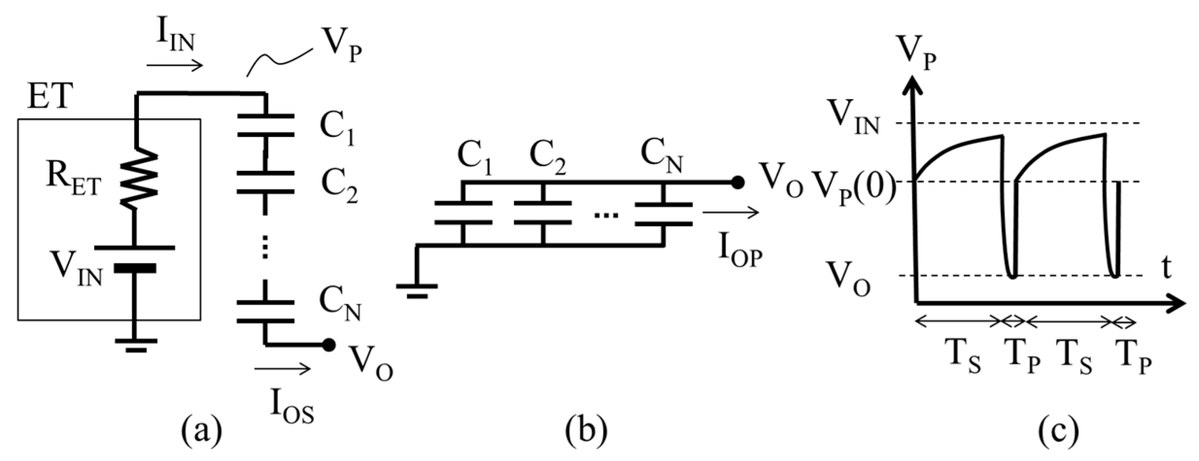
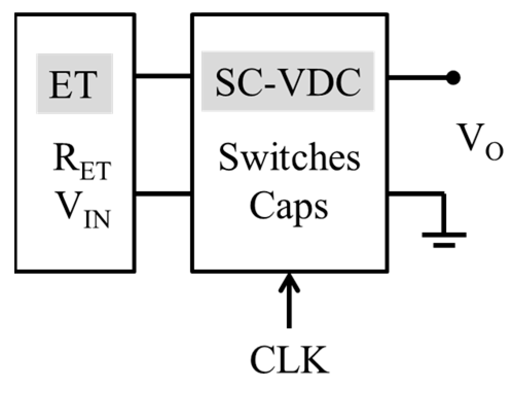
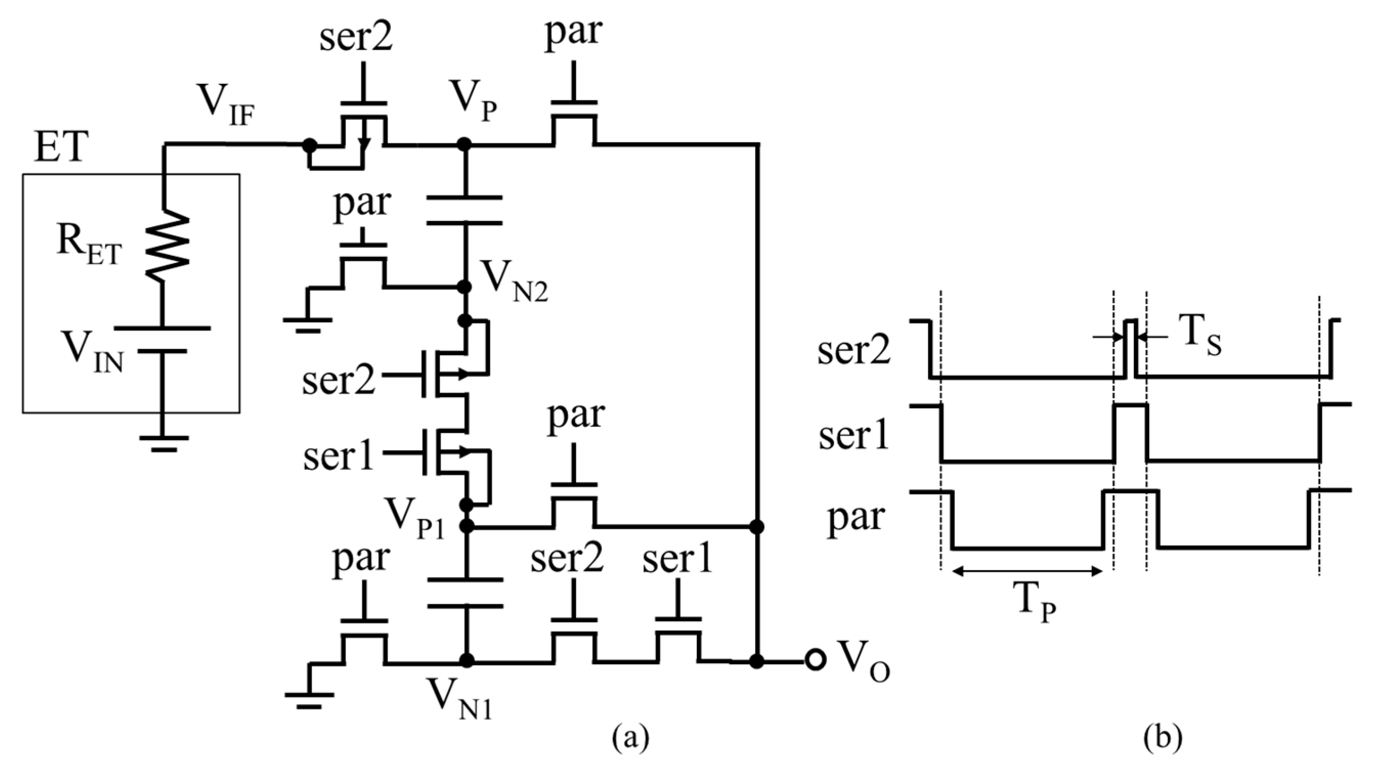
2. Circuit Model
2.1. Ideal Case with No RET
2.2. Practical Case with Large RET
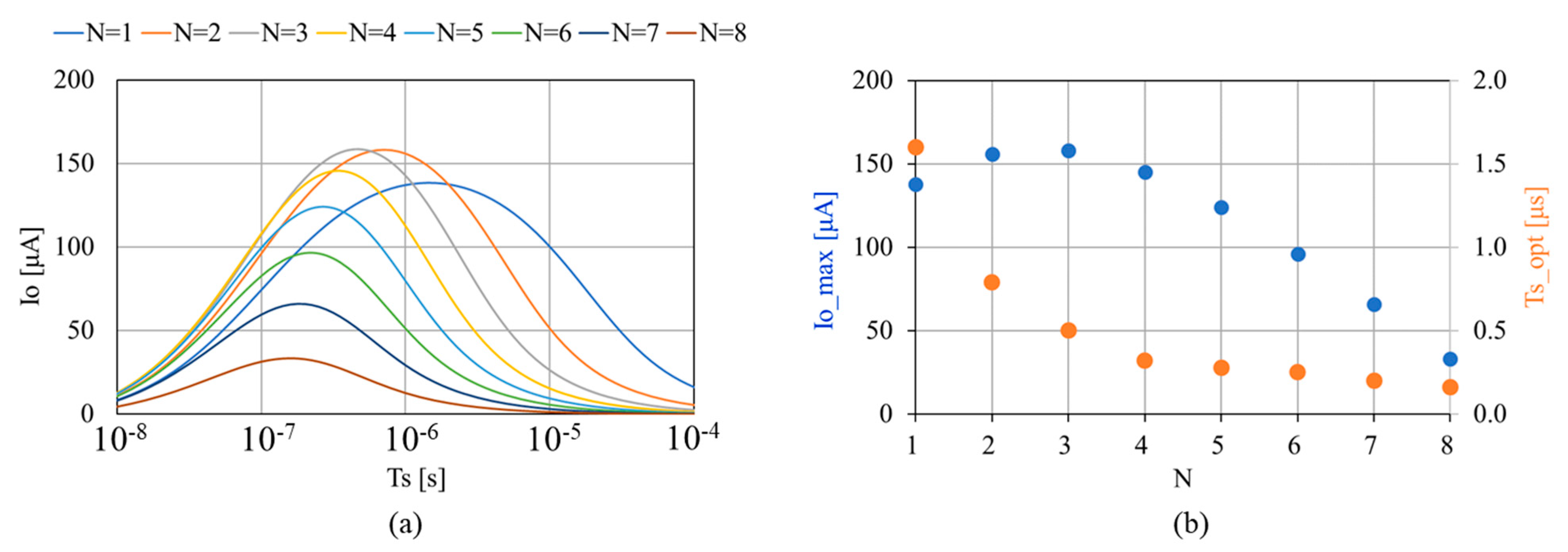
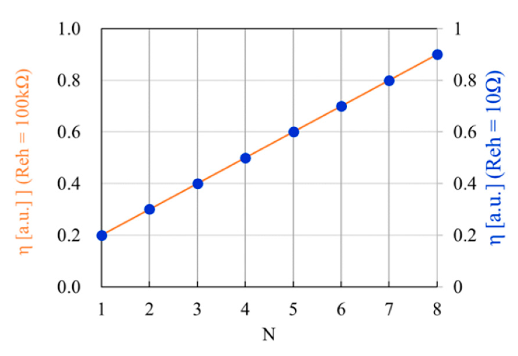
2.3. Characteristics of SC-VDC for Highly Resistive ET
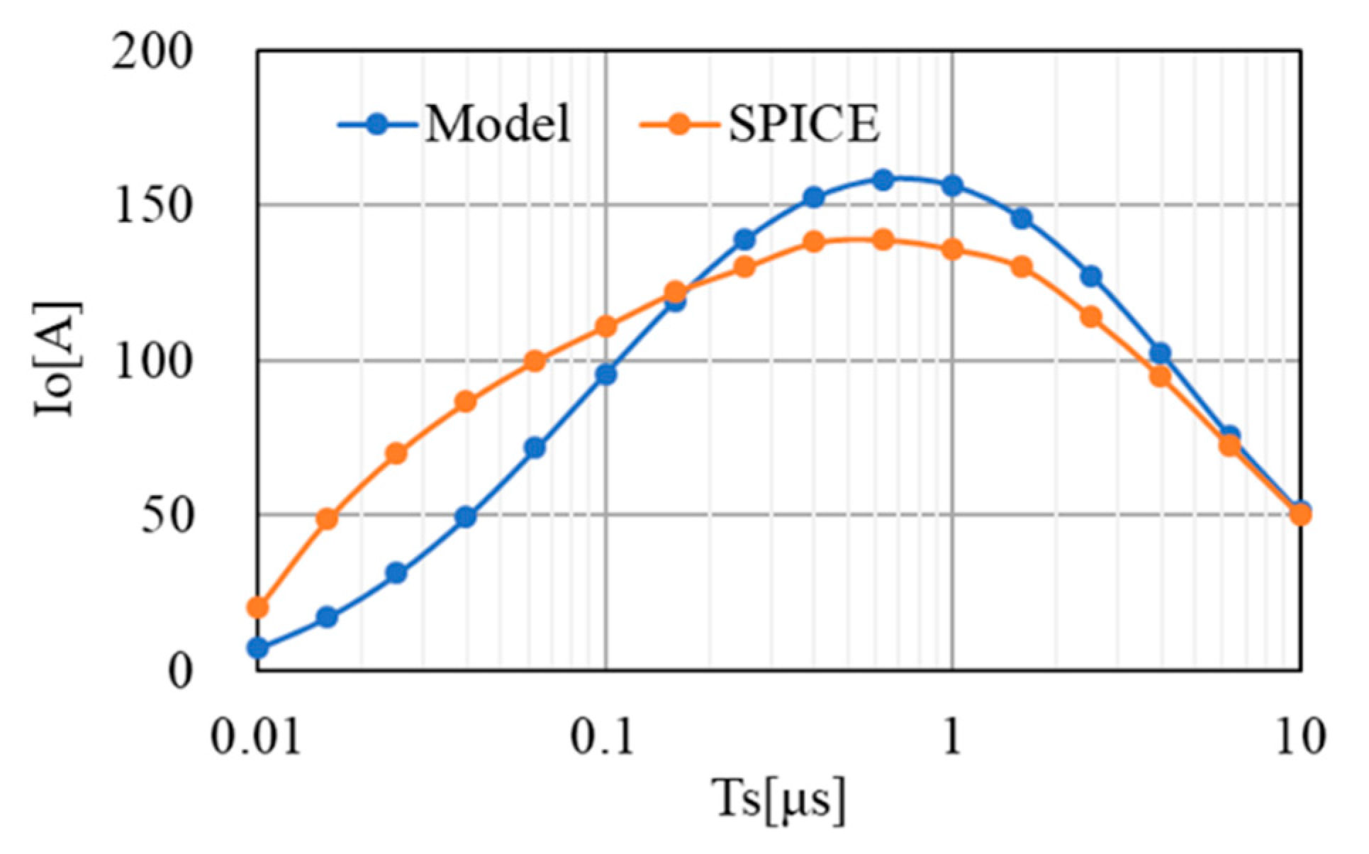
2.4. Validation of the Model
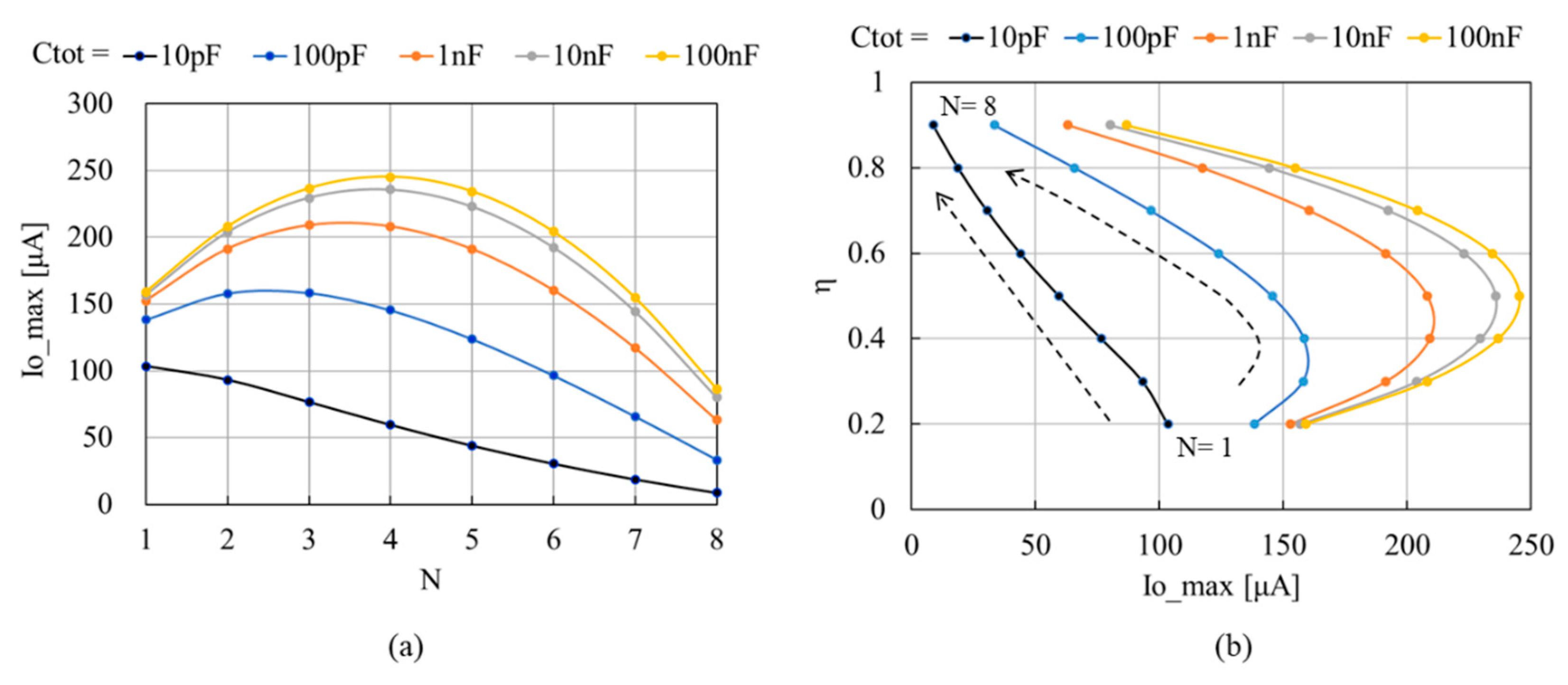
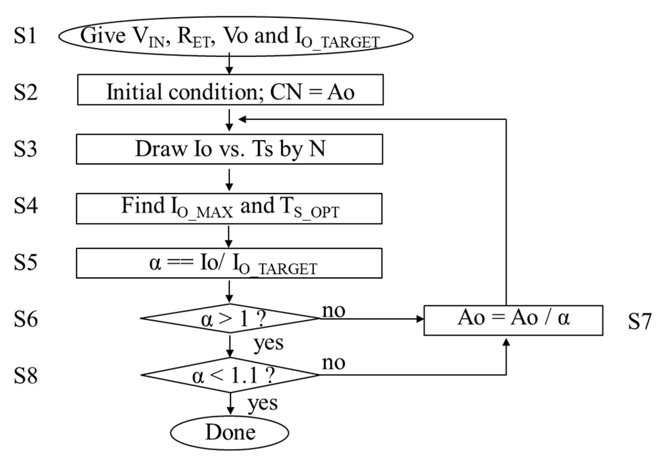
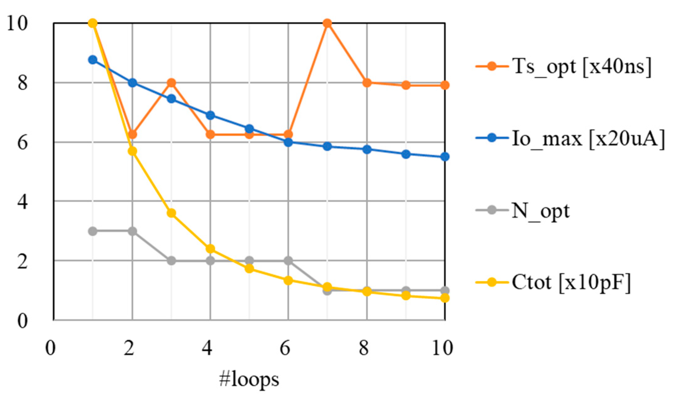
3. Optimum Design Flow
4. Conclusions
Author Contributions
Funding
Acknowledgments
Conflicts of Interest
References
- Kazmiersuki, T.; Beedy, S. Energy Harvesting Systems: Principles, Modeling and Applications; Springer: Berlin/Heidelberg, Germany, 2010; pp. 1–78. [Google Scholar]
- Fu, Q.; Suzuki, Y.; Suzuki, Y. MEMS vibration electret energy harvester with combined electrodes. In Proceedings of the 2014 IEEE 27th International Conference on Micro Electro Mechanical Systems (MEMS), San Francisco, CA, USA, 26–30 January 2014; IEEE: Piscataway, NJ, USA, 2014; pp. 409–412. [Google Scholar] [CrossRef]
- Hashiguchi, G. Electromechanical theory of microelectromechanical devices. IEICE Electron. Express 2014, 11, 20142007. [Google Scholar] [CrossRef] [Green Version]
- Stanzione, S.; Van Liempd, C.; Van Schaijk, R.; Naito, Y.; Yazicioglu, R.F.; Van Hoof, C. A self-biased 5-to-60 V input voltage and 25-to-1600 µW integrated DC-DC buck converter with fully analog MPPT algorithm reaching up to 88% end-to-end efficiency. In Proceedings of the 2013 IEEE International Solid-State Circuits Conference Digest of Technical Papers, San Francisco, CA, USA, 17–21 February 2013; IEEE: Piscataway, NJ, USA, 2013; pp. 74–75. [Google Scholar]
- Stanzione, S.; Van Liempd, C.; Nabeto, M.; Yazicioglu, F.R.; Van Hoof, C. 20.8 a 500 nW batteryless integrated electrostatic energy harvester interface based on a DC-DC converter with 60 V maximum input voltage and operating from 1 μW available power, including MPPT and cold start. In Proceedings of the 2015 IEEE International Solid-State Circuits Conference—(ISSCC) Digest of Technical Papers, San Francisco, CA, USA, 22–26 February 2015; IEEE: Piscataway, NJ, USA, 2015; pp. 1–3. [Google Scholar]
- Wang, C.-C.; Tolentino, L.K.S.; Chen, P.-C.; Hizon, J.R.E.; Yen, C.-K.; Pan, C.-T.; Hsueh, Y.-H. A 40-nm CMOS Piezoelectric Energy Harvesting IC for Wearable Biomedical Applications. Electronics 2021, 10, 649. [Google Scholar] [CrossRef]
- Lai, L.; Zhang, R.; Cheng, K.; Xia, Z.; Wei, C.; Wei, K.; Luo, W.; Liu, X. Monolithic integrated high frequency GaN DC-DC buck converters with high power density controlled by current mode logic level signal. Electronics 2020, 9, 1540. [Google Scholar] [CrossRef]
- Ishida, Y.; Tanzawa, T. A Fully Integrated AC-DC Converter in 1 V CMOS for Electrostatic Vibration Energy Transducer with an Open Circuit Voltage of 10 V. Electronics 2021, 10, 1185. [Google Scholar] [CrossRef]
- Meyvaert, H.; Pique, G.V.; Karadi, R.; Bergveld, H.J.; Steyaert, M.S.J. A Light-Load-Efficient 11/1 Switched-Capacitor DCDC Converter with 94.7% Efficiency While Delivering 100 mW at 3.3 V. IEEE J. Solid State Circuits 2015, 50, 2849–2860. [Google Scholar] [CrossRef] [Green Version]
- Tanzawa, T. Design of DC-DC Switched-Capacitor Voltage Multiplier driven by DC Energy Transducer. In Proceedings of the IEEE International Conference on Electronics, Circuits and Systems (ICECS) 2014, Marseille, France, 7–10 December 2014; IEEE: Piscataway, NJ, USA, 2015; pp. 327–330. [Google Scholar] [CrossRef]
- Tanzawa, T.; Atsumi, S. Optimization of word-line booster circuits for low-voltage Flash memories. IEEE J. Solid State Circuits 1999, 34, 1091–1098. [Google Scholar] [CrossRef]
- Tanzawa, T. On-Chip High-Voltage Generator Design: Design Methodology for Charge Pumps, 2nd ed.; Springer: Cham, Switzerland, 2016. [Google Scholar] [CrossRef]
- Le, H.-P.; Sanders, S.R.; Alon, E. Design techniques for fully integrated switched-capacitor DC-DC converters. IEEE J. Solid State Circuits 2011, 46, 2120–2131. [Google Scholar] [CrossRef]
- Tanzawa, T. On two-phase switched-capacitor multipliers with minimum circuit area. IEEE Trans. Circuits Syst. I Regul. Pap. 2010, 57, 2602–2608. [Google Scholar] [CrossRef]


| Parameters | Default Value |
|---|---|
| VIN | 10 V |
| RET | 100 kΩ (10 Ω for reference) |
| VO | 1.0 V |
| C | 1.0 nF |
| N | 4 |
| TS | 10 μs |
| TP | 100 ns |
Publisher’s Note: MDPI stays neutral with regard to jurisdictional claims in published maps and institutional affiliations. |
© 2022 by the authors. Licensee MDPI, Basel, Switzerland. This article is an open access article distributed under the terms and conditions of the Creative Commons Attribution (CC BY) license (https://creativecommons.org/licenses/by/4.0/).
Share and Cite
Demura, Y.; Tanzawa, T. Design of Switched-Capacitor DC-DC Voltage-Down Converters Driven by Highly Resistive Energy Transducer. Electronics 2022, 11, 1874. https://doi.org/10.3390/electronics11121874
Demura Y, Tanzawa T. Design of Switched-Capacitor DC-DC Voltage-Down Converters Driven by Highly Resistive Energy Transducer. Electronics. 2022; 11(12):1874. https://doi.org/10.3390/electronics11121874
Chicago/Turabian StyleDemura, Yosuke, and Toru Tanzawa. 2022. "Design of Switched-Capacitor DC-DC Voltage-Down Converters Driven by Highly Resistive Energy Transducer" Electronics 11, no. 12: 1874. https://doi.org/10.3390/electronics11121874
APA StyleDemura, Y., & Tanzawa, T. (2022). Design of Switched-Capacitor DC-DC Voltage-Down Converters Driven by Highly Resistive Energy Transducer. Electronics, 11(12), 1874. https://doi.org/10.3390/electronics11121874